JP2012142683A - Piezoelectric device - Google Patents
Piezoelectric device Download PDFInfo
- Publication number
- JP2012142683A JP2012142683A JP2010292323A JP2010292323A JP2012142683A JP 2012142683 A JP2012142683 A JP 2012142683A JP 2010292323 A JP2010292323 A JP 2010292323A JP 2010292323 A JP2010292323 A JP 2010292323A JP 2012142683 A JP2012142683 A JP 2012142683A
- Authority
- JP
- Japan
- Prior art keywords
- thermistor element
- piezoelectric vibration
- main surface
- thermistor
- substrate
- Prior art date
- Legal status (The legal status is an assumption and is not a legal conclusion. Google has not performed a legal analysis and makes no representation as to the accuracy of the status listed.)
- Granted
Links
Images


Abstract
Description
本発明は、電子機器等に用いられる圧電デバイスに関するものである。 The present invention relates to a piezoelectric device used in electronic equipment and the like.
従来の圧電デバイスは、その例として素子搭載部材、圧電振動素子、サーミスタ素子、蓋部材とから主に構成されている構造が知られている(例えば、特許文献1を参照)。
素子搭載部材は、基板部と第1の枠部と第2の枠部で構成されている。
基板部の主面に第2の枠部が設けて、第2の凹部空間が形成され、第2の枠部に第1の枠部を設けて第1の凹部空間が形成されている。
第1の凹部空間内に露出する第2の枠部の一方の主面には、2個一対の圧電振動素子搭載パッドが設けられている。
第2の凹部空間内に露出する基板部の一方の主面には、サーミスタ素子搭載パッドが設けられている。
また、基板部の他方の主面の4隅には、外部接続用電極端子が設けられている。
この圧電振動素子搭載パッド上には、導電性接着剤を介して電気的に接続される一対の励振用電極を表裏主面に有した圧電振動素子が搭載されている。この圧電振動素子を囲繞する素子搭載部材の第1の枠部の頂面には金属製の蓋部材を被せられ、接合されている。これにより第1の凹部空間と第2の凹部空間が気密封止されている。
また、サーミスタ素子搭載パッド上には、半田等の導電性接合材を介して接続されるサーミスタ素子が搭載されている。
サーミスタ素子は、その温度での抵抗値が、外部接続用電極端子を介して圧電デバイスの外へ出力される。この出力された抵抗値の変化から電圧が変化するため、電圧と温度との関係により、出力された抵抗値を電圧に換算することで、そのときの電圧から温度情報を得ることができる。例えば、電子機器等のメインIC内で温度情報に換算することができる。
また、外部接続用電極端子は、2個一対の水晶振動素子用電極端子と、2個一対のサーミスタ素子用電極端子により構成されている。その水晶振動素子用電極端子は、対角に配置されている。また、サーミスタ素子用電極端子も同様に、対角に配置されている。
As a conventional piezoelectric device, for example, a structure mainly composed of an element mounting member, a piezoelectric vibration element, a thermistor element, and a lid member is known (see, for example, Patent Document 1).
The element mounting member includes a substrate part, a first frame part, and a second frame part.
A second frame portion is provided on the main surface of the substrate portion to form a second recess space, and a first frame portion is provided to the second frame portion to form a first recess space.
Two pairs of piezoelectric vibration element mounting pads are provided on one main surface of the second frame exposed in the first recess space.
A thermistor element mounting pad is provided on one main surface of the substrate portion exposed in the second recess space.
Also, external connection electrode terminals are provided at the four corners of the other main surface of the substrate portion.
On the piezoelectric vibration element mounting pad, a piezoelectric vibration element having a pair of excitation electrodes electrically connected via a conductive adhesive on the front and back main surfaces is mounted. The top surface of the first frame portion of the element mounting member surrounding the piezoelectric vibration element is covered with a metal lid member and joined. Thereby, the first recess space and the second recess space are hermetically sealed.
A thermistor element connected via a conductive bonding material such as solder is mounted on the thermistor element mounting pad.
The thermistor element outputs a resistance value at that temperature to the outside of the piezoelectric device via the external connection electrode terminal. Since the voltage changes due to the change in the output resistance value, the temperature information can be obtained from the voltage at that time by converting the output resistance value into a voltage according to the relationship between the voltage and the temperature. For example, it can be converted into temperature information in a main IC such as an electronic device.
In addition, the external connection electrode terminal includes two pairs of crystal vibration element electrode terminals and two pairs of thermistor element electrode terminals. The crystal vibration element electrode terminals are arranged diagonally. Similarly, the thermistor element electrode terminals are also arranged diagonally.
しかしながら、従来の圧電デバイスにおいては、2個一対の圧電振動素子用電極端子と2個一対のサーミスタ素子用電極端子とによって外部接続用電極端子が構成されているので、グランド端子が設けられていない。よって、蓋部材が電気的に浮いた状態になっていた。このように前記蓋部材に外部から筐体などのグランドが近づいた場合、圧電振動素子の励振用電極と筐体との間で浮遊容量が生じ、圧電振動素子の発振周波数が変動してしまうといった課題があった。 However, in the conventional piezoelectric device, since the electrode terminal for external connection is constituted by the two pairs of electrode terminals for piezoelectric vibration elements and the two pairs of electrode terminals for thermistor elements, no ground terminal is provided. . Therefore, the lid member was in an electrically floating state. As described above, when a ground such as a housing approaches the lid member from the outside, stray capacitance is generated between the excitation electrode of the piezoelectric vibration element and the housing, and the oscillation frequency of the piezoelectric vibration element fluctuates. There was a problem.
また、従来の圧電デバイスにおいては、2個一対の圧電振動素子用電極端子と2個一対のサーミスタ素子用電極端子とによって外部接続用電極端子が構成されているので、グランド端子が設けられていないことによって、サーミスタ素子にノイズが重畳してしまうといった課題もあった。 Moreover, in the conventional piezoelectric device, since the electrode terminal for external connection is comprised by the electrode terminal for two pairs of piezoelectric vibration elements and the electrode terminal for two pairs of thermistor elements, the ground terminal is not provided. As a result, there is a problem that noise is superimposed on the thermistor element.
本発明は上記課題に鑑みてなされたものであり、圧電振動素子の発振周波数の変動を低減することができる圧電デバイスを提供することを課題とする。 This invention is made | formed in view of the said subject, and makes it a subject to provide the piezoelectric device which can reduce the fluctuation | variation of the oscillation frequency of a piezoelectric vibration element.
本発明の圧電デバイスは、基板部と、この基板部の一方の主面に設けられる第1の枠部と、基板部の他方の主面に設けられる第2の枠部とからなる素子搭載部材と、基板部と第1の枠部とで形成される第1の凹部空間内に露出した基板部の主面に設けられた圧電振動素子搭載パッドに搭載されている圧電振動素子と、基板部と第2の枠部とで形成される第2の凹部空間内に露出した基板部の主面に設けられたサーミスタ素子搭載パッドに搭載されているサーミスタ素子と、第1の凹部空間を気密封止する蓋部材と、第2の枠部の基板部の他方の主面と同一方向を向く面の4角に2個一対の圧電振動素子用電極端子と2個一対のサーミスタ素子用電極端子とから構成される外部接続用電極端子と、備え、2個一対のサーミスタ素子用電極端子の1つが蓋部材と電気的に接続され、グランドと接続されることを特徴とするものである。 The piezoelectric device of the present invention is an element mounting member comprising a substrate portion, a first frame portion provided on one main surface of the substrate portion, and a second frame portion provided on the other main surface of the substrate portion. A piezoelectric vibration element mounted on a piezoelectric vibration element mounting pad provided on a main surface of the substrate portion exposed in the first recess space formed by the substrate portion and the first frame portion, and the substrate portion The thermistor element mounted on the thermistor element mounting pad provided on the main surface of the substrate portion exposed in the second recess space formed by the second frame portion and the first recess space are hermetically sealed A pair of piezoelectric vibration element electrode terminals and two pair of thermistor element electrode terminals at four corners of a surface facing the same direction as the other main surface of the substrate portion of the second frame portion, An electrode terminal for external connection composed of two electrode terminals for a pair of thermistor elements Tsugafuta member and is electrically connected, is characterized in being connected to the ground.
前記素子搭載部材に前記圧電振動素子と前記サーミスタ素子とを搭載した状態で、平面視で前記圧電振動素子に設けられる励振用電極の平面内に前記サーミスタ素子を位置させて構成されていることを特徴とするものである。 In a state where the piezoelectric vibration element and the thermistor element are mounted on the element mounting member, the thermistor element is positioned in a plane of an excitation electrode provided on the piezoelectric vibration element in a plan view. It is a feature.
本発明の圧電デバイスによれば、2個一対のサーミスタ素子用電極端子の1つが蓋部材と電気的に接続されていることによって、その1つのサーミスタ素子用電極端子をグランドに接続することで、蓋部材がグランドに接続されることになる。よって、前記蓋部材に外部から筐体などのグランドが近づいても、圧電振動素子の励振用電極と筐体との間で浮遊容量が生じないため、圧電振動素子の発振周波数が変動することを低減することができる。 According to the piezoelectric device of the present invention, one of the two pairs of thermistor element electrode terminals is electrically connected to the lid member, thereby connecting the one thermistor element electrode terminal to the ground. The lid member is connected to the ground. Therefore, even if a ground such as a housing approaches the lid member from the outside, no stray capacitance is generated between the excitation electrode of the piezoelectric vibration element and the housing, and therefore the oscillation frequency of the piezoelectric vibration element varies. Can be reduced.
また、本発明の圧電デバイスによれば、2個一対のサーミスタ素子用電極端子の1つが蓋部材と電気的に接続され、その1つのサーミスタ素子用電極端子をグランドに接続し、前記素子搭載部材に前記圧電振動素子と前記サーミスタ素子とを搭載した状態で、平面視で前記圧電振動素子に設けられる励振用電極の平面内に前記サーミスタ素子を位置させて構成されていることによって、圧電振動素子の励振用電極及び蓋部材と、グランドと接続されているサーミスタ素子用電極端子とで挟まれた状態になるために、サーミスタ素子にノイズが重畳することを低減することができる。 According to the piezoelectric device of the present invention, one of the two pairs of thermistor element electrode terminals is electrically connected to the lid member, the one thermistor element electrode terminal is connected to the ground, and the element mounting member In the state where the piezoelectric vibration element and the thermistor element are mounted on the piezoelectric vibration element, the thermistor element is positioned in the plane of the excitation electrode provided on the piezoelectric vibration element in a plan view. Therefore, it is possible to reduce the superposition of noise on the thermistor element.
以下、本発明を添付図面に基づいて詳細に説明する。尚、圧電振動素子に水晶を用いた場合について説明する。 Hereinafter, the present invention will be described in detail with reference to the accompanying drawings. A case where quartz is used for the piezoelectric vibration element will be described.
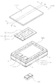
本発明の実施形態に係る圧電デバイス100は、図1及び図2に示すように、素子搭載部材110と圧電振動素子120と蓋部材130とサーミスタ素子140で主に構成されている。この圧電デバイス100は、前記素子搭載部材110に形成されている第1の凹部空間K1内に圧電振動素子120が搭載され、第2の凹部空間K2内には、サーミスタ素子140が搭載されている。その第1の凹部空間K1が蓋部材130により気密封止された構造となっている。
As shown in FIGS. 1 and 2, the
圧電振動素子120は、図1及び図2に示すように、水晶素板121に励振用電極122を被着形成したものであり、外部からの交番電圧が励振用電極122を介して水晶素板121に印加されると、所定の振動モード及び周波数で励振を起こすようになっている。
水晶素板121は、人工水晶体から所定のカットアングルで切断し外形加工を施された概略平板状で平面形状が例えば四角形となっている。
励振用電極122は、前記水晶素板121の表裏両主面に金属を所定のパターンで被着・形成したものである。
このような圧電振動素子120は、その両主面に被着されている励振用電極122から延出する引き出し電極123と第1の凹部空間K1内底面に形成されている圧電振動素子搭載パッド111とを、導電性接着剤DSを介して電気的且つ機械的に接続することによって第1の凹部空間K1に搭載される。このときの引き出し電極123が設けられた一辺とは反対側の自由端となる端辺を圧電振動素子120の先端部とする。
As shown in FIGS. 1 and 2, the
The
The excitation electrode 122 is formed by depositing and forming a metal in a predetermined pattern on both the front and back main surfaces of the
Such a
図1〜図2に示すサーミスタ素子140は、温度変化によって電気抵抗が顕著な変化を示すものであり、この抵抗値の変化から電圧が変化するため、抵抗値と電圧との関係及び電圧と温度との関係により、出力された抵抗値を電圧に換算することで、換算して得られた電圧から温度情報を得ることができる。サーミスタ素子140は、その温度での抵抗値が、外部接続用電極端子Gを介して圧電デバイス100の外へ出力されることにより、例えば、電子機器等のメインIC(図示せず)で出力された抵抗値を電圧に換算することで温度情報を得ることができる。
サーミスタ素子140は、図2に示すように、素子搭載部材110の第2の凹部空間K2内に露出した後述する基板部110aに設けられたサーミスタ素子搭載パッド112に半田等の導電性接合材HDを介して搭載されている。
The
As shown in FIG. 2, the
サーミスタ素子140は、図3及び図4に示すように、素子搭載部材110の第2の凹部空間K2の長辺側壁部と平行になるように搭載されている。つまり、サーミスタ素子140は、素子搭載部材110の長辺側外周縁部と平行になるように搭載されている。
また、サーミスタ素子140は、図3に示すように、前記素子搭載部材110に前記圧電振動素子120と前記サーミスタ素子140とを搭載した状態で、平面視で前記圧電振動素子120に設けられる励振用電極122の平面内に位置するように、第2の凹部空間K2内に搭載されている。つまり、図3に示すように、サーミスタ素子140は、圧電振動素子120の励振用電極122の直下にある第2の凹部空間K2内に搭載され、前記励振用電極122からはみ出ることがなく、平面視で励振用電極122が設けられている面積内に設けられている。
As shown in FIGS. 3 and 4, the
Further, as shown in FIG. 3, the
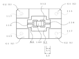
図1〜図2に示すように、素子搭載部材110は、基板部110aと、第1の枠部110b、第2の枠部110cとで主に構成されている。
この素子搭載部材110は、前記基板部110aの一方の主面に第1の枠部110bが設けられて、第1の凹部空間K1が形成されている。また、素子搭載部材110の他方の主面に第2の枠部110cが設けられて、第2の凹部空間K2が形成されている。
尚、この素子搭載部材110を構成する基板部110a及び第2の枠部110cは、例えばアルミナセラミックス、ガラス−セラミックス等のセラミック材料を複数積層することよって形成されている。
第1の枠部110bは、42アロイやコバール等の金属から成り、中心が打ち抜かれた枠状になっている。
また、第1の枠部110bは、基板部110aの一方の主面の外周を囲繞するように設けられた封止用導体膜HB上にロウ付けなどにより接続される。
第1の凹部空間K1内で露出した基板部110aの一方の主面には、2個一対の圧電振動素子搭載パッド111が設けられている。
また、図1〜図3に示すように素子搭載部材110は、基板部110aの他方の主面と第2の枠部110cによって第2の凹部空間K2が形成されている。
第2の凹部空間K2内で露出した基板部110aの他方の主面には、サーミスタ素子搭載パッド112が設けられている。
As shown in FIGS. 1 to 2, the
In the
In addition, the board | substrate part 110a and the 2nd frame part 110c which comprise this
The first frame portion 110b is made of a metal such as 42 alloy or Kovar, and has a frame shape with a punched center.
The first frame portion 110b is connected to the sealing conductor film HB provided so as to surround the outer periphery of one main surface of the substrate portion 110a by brazing or the like.
Two pairs of piezoelectric vibration element mounting pads 111 are provided on one main surface of the substrate portion 110a exposed in the first recess space K1.
1 to 3, the
A thermistor
前記素子搭載部材110の第2の枠部110cの圧電振動素子搭載パッド111が設けられている面とは反対側の主面の4隅には、外部接続用電極端子Gが設けられている。
外部接続用電極端子Gは、2個一対の圧電振動素子用電極端子G1と2個一対のサーミスタ素子用電極端子G2により構成されている。
2個一対の圧電振動素子用電極端子G1は、前記素子搭載部材110の第2の枠部110cの他方の主面の対角に設けられている。
また、2個一対のサーミスタ素子用電極端子G2は第2の枠部110cの前記圧電振動素子用電極端子G1が設けられている位置と異なる2つの隅部に設けられている。つまり、前記サーミスタ素子用電極端子G2は、前記圧電振動素子用電極端子G1が設けられている対角とは異なる第2の枠部110cの対角に設けられている。
External connection electrode terminals G are provided at the four corners of the main surface opposite to the surface on which the piezoelectric vibration element mounting pad 111 of the second frame portion 110c of the
The external connection electrode terminal G includes two pairs of piezoelectric vibration element electrode terminals G1 and two pairs of thermistor element electrode terminals G2.
The two pairs of piezoelectric vibration element electrode terminals G <b> 1 are provided diagonally to the other main surface of the second frame portion 110 c of the
The two pairs of thermistor element electrode terminals G2 are provided at two corners of the second frame 110c different from the positions where the piezoelectric vibration element electrode terminals G1 are provided. In other words, the thermistor element electrode terminal G2 is provided at a diagonal of the second frame portion 110c different from the diagonal at which the piezoelectric vibration element electrode terminal G1 is provided.
張り出し部K3は、図4に示すように、前記素子搭載部材110の前記第2の枠部110cの同一辺側で隣接しあう2つの外部接続用電極端子G間に張り出すようにして設けられている。
前記張り出し部K3は、隣接しあう2つ外部接続用電極端子Gの間に、第2の凹部空間K2の一部が延出するようにして設けられている。
この張り出し部K3には、前記サーミスタ素子用配線パターン116の一部が露出するようにして設けられている。また、前記張り出し部K3の長辺方向の長さL1は、約100〜200μmである。
As shown in FIG. 4, the projecting portion K3 is provided so as to project between two external connection electrode terminals G adjacent to each other on the same side of the second frame portion 110c of the
The protruding portion K3 is provided between two adjacent external connection electrode terminals G so that a part of the second recessed space K2 extends.
The overhang portion K3 is provided so that a part of the thermistor
圧電振動素子搭載パッド111といずれかの外部接続用電極端子Gは、前記素子搭載部材110の第2の凹部空間K2内の基板部110aに形成された部分を有する圧電振動素子用配線パターン113と、基板部110aに設けられた第1のビア導体114と、基板部110a及び第2の枠部110cの内部に形成された第2のビア導体115により接続されている。
つまり、図5及び図6に示すように、圧電振動素子搭載パッド111は、第1のビア導体114を介して圧電振動素子用配線パターン113の一端と接続されている。また、圧電振動素子用配線パターン113の他端は、第2のビア導体115を介して圧電振動素子用電極端子G1と接続されている。よって、圧電振動素子搭載パッド111は、圧電振動素子用電極端子G1と電気的に接続されることになる。
The piezoelectric vibration element mounting pad 111 and any one of the external connection electrode terminals G include a piezoelectric vibration element wiring pattern 113 having a portion formed on the substrate portion 110a in the second recess space K2 of the
That is, as shown in FIGS. 5 and 6, the piezoelectric vibration element mounting pad 111 is connected to one end of the piezoelectric vibration element wiring pattern 113 via the first via conductor 114. The other end of the piezoelectric vibration element wiring pattern 113 is connected to the piezoelectric vibration element electrode terminal G <b> 1 via the second via
また、サーミスタ素子搭載パッド112とサーミスタ素子用電極端子G2は、前記素子搭載部材110の第2の凹部空間K2内の基板部110aに形成された部分を有するサーミスタ素子用配線パターン116と第2の枠部110cの内部に形成された第3のビア導体117により接続されている。
つまり、図6(a)及び図6(b)に示すようにサーミスタ素子搭載パッド112は、サーミスタ素子用配線パターン116の一端と接続されている。また、サーミスタ素子用配線パターン116の他端は、第3のビア導体117を介してサーミスタ素子用電極端子G2と接続されている。よって、サーミスタ素子用搭載パッド112は、サーミスタ素子用電極端子G2と電気的に接続されることになる。
Further, the thermistor
That is, as shown in FIGS. 6A and 6B, the thermistor
第2の凹部空間K2内底面に露出している2個一対のサーミスタ素子用配線パターン116は、図6(b)に示すように、前記張り出し部K3に素子搭載部材110の長辺側外周縁部と平行で、搭載後のサーミスタ素子140と平行になるように設けられている。
The two pairs of thermistor
また、前記第2の凹部空間K2内底面に露出している2個一対のサーミスタ素子用配線パターン116の長さL2が等しくなっている。つまり、2個一対のサーミスタ素子用配線パターン116の長さL2が同じ長さになっている。
第2の凹部空間K2内底面に露出している2個一対のサーミスタ素子用配線パターン116の長さL2は、約200〜250μmである。
Further, the lengths L2 of the two pairs of thermistor
The length L2 of the two pairs of thermistor
また、図2及び図5(a)に示すように、第1の枠部110bは、第3のビア導体117と第4のビア導体118とを介して、2個一対のサーミスタ素子用電極端子G2と電気的に接続されることになる。
つまり、第1の枠部110bとサーミスタ素子140の一端は、第3のビア導体117を介して電気的に接続されることになる。
また、2個一対のサーミスタ素子用電極端子G2の内の1つは、蓋部材130と電気的に接続され、グランドと接続されることになる。
Further, as shown in FIGS. 2 and 5A, the first frame portion 110b has two pairs of thermistor element electrode terminals via a third via
That is, one end of the first frame portion 110 b and the
One of the two thermistor element electrode terminals G2 is electrically connected to the
蓋部材130は、例えば、Fe−Ni合金(42アロイ)やFe−Ni−Co合金(コバール)などからなる。このような蓋部材130は、第1の凹部空間K1を、窒素ガスや真空などで気密的に封止される。具体的には、蓋部材130は、所定雰囲気で、素子搭載部材110の第1の枠部110b上に載置され、第1の枠部110bの表面の金属と蓋部材130の金属の一部とが溶接されるように所定電流を印加してシーム溶接を行うことにより、第1の枠部110bに接合される。
蓋部材130は、図2(b)に示すように、第1の枠部110bを介して、第4のビア導体118と接続されている。また、この第4のビア導体118は、第3のビア導体117の1つを介して、2個一対のサーミスタ素子用電極端子G2の内の1つと接続されている。つまり、蓋部材130は、2個一対のサーミスタ素子用電極端子G2の内の1つと電気的に接続される。
また、2個一対のサーミスタ素子用電極端子G2の内の1つは、グランドに接続される。つまり、蓋部材130は、2個一対のサーミスタ素子用電極端子G2の内の1つを介して、グランドと接続されることになる。
The
As shown in FIG. 2B, the
One of the two thermistor element electrode terminals G2 is connected to the ground. That is, the
前記導電性接着剤DSは、シリコーン樹脂等のバインダーの中に導電フィラーとして導電性粉末が含有されているものであり、導電性粉末としては、アルミニウム(Al)、モリブデン(Mo)、タングステン(W)、白金(Pt)、パラジウム(Pd)、銀(Ag)、チタン(Ti)、ニッケル(Ni)、ニッケル鉄(NiFe)、のうちのいずれかまたはこれらの組み合わせを含むものが用いられている。 The conductive adhesive DS contains a conductive powder as a conductive filler in a binder such as a silicone resin. As the conductive powder, aluminum (Al), molybdenum (Mo), tungsten (W ), Platinum (Pt), palladium (Pd), silver (Ag), titanium (Ti), nickel (Ni), nickel iron (NiFe), or a combination thereof is used. .
尚、前記素子搭載部材110は、アルミナセラミックスから成る場合、所定のセラミック材料粉末に適当な有機溶剤等を添加・混合して得たセラミックグリーンシートの表面に圧電振動素子搭載パッド111、サーミスタ素子搭載パッド112、封止用導体膜HB、外部接続用電極端子G等となる導体ペーストを、また、セラミックグリーンシートに打ち抜き等を施して予め穿設しておいた貫通孔内に第1のビア導体114、第2のビア導体115、第3のビア導体117等となる導体ペーストを従来周知のスクリーン印刷によって塗布するとともに、これを複数枚積層してプレス成形した後、高温で焼成することにより製作される。
When the
本発明の圧電デバイス100によれば、2個一対のサーミスタ素子用電極端子G2の1つが蓋部材130と電気的に接続されていることによって、その1つのサーミスタ素子用電極端子G2をグランドに接続することで、蓋部材130がグランドに接続されることになる。よって、前記蓋部材130に外部から筐体(図示せず)などのグランドが近づいても、圧電振動素子120の励振用電極122と筐体(図示せず)との間で浮遊容量が生じないため、発振周波数が変動することを低減することができる。
According to the
本発明の圧電デバイス100によれば、サーミスタ素子140は、素子搭載部材110に圧電振動素子120とサーミスタ素子140とを搭載した状態で、平面視で圧電振動素子120に設けられる励振用電極122の平面内に前記サーミスタ素子140を位置させ、2個一対のサーミスタ素子用電極端子G2の1つが蓋部材130と電気的に接続され、その1つのサーミスタ素子用電極端子G2をグランドに接続することで、励振用電極122とグランドと接続されているサーミスタ素子用電極端子G2とで挟まれた状態になるために、従来の圧電デバイスに比べてサーミスタ素子140にノイズが重畳することを低減し、正確なサーミスタ素子140の値を出力することができる。
つまり、蓋部材130及び励振用電極122と、グランドに接続されているサーミスタ素子用電極端子G2とによって、挟みこむようにしてサーミスタ素子140がノイズから保護されるので、従来の圧電デバイスに比べてサーミスタ素子140にノイズが重畳することを低減し、正確なサーミスタ素子140の値を出力することができる。
また、サーミスタ素子140から正確な出力値を出力することができるので、サーミスタ素子140から出力された抵抗値を換算することで得られた電圧から温度情報を得ることができる。このようにして得られた温度情報と、実際の圧電振動素子120の周囲の温度情報との差異を低減することが可能となる。
According to the
That is, the
In addition, since an accurate output value can be output from the
尚、本発明は前記実施形態に限定されるものではなく、本発明の要旨を逸脱しない範囲において種々の変更、改良等が可能である。
例えば、前記した本実施形態では、圧電振動素子120を構成する圧電素材として水晶を用いた場合を説明したが、他の圧電素材として、ニオブ酸リチウム、タンタル酸リチウムまたは、圧電セラミックスを圧電素材として用いた圧電振動素子でも構わない。
In addition, this invention is not limited to the said embodiment, A various change, improvement, etc. are possible in the range which does not deviate from the summary of this invention.
For example, in the above-described embodiment, the case where crystal is used as the piezoelectric material constituting the
また、前記した実施形態では、素子搭載部材110を構成する第1の枠部110bは、42アロイやコバール等の金属から成り、中心が打ち抜かれた枠状になっている場合を説明したが、第1の枠部110bがセラミック材料からなり、中心が打ち抜かれた枠状になっていても構わない。また、その際には、第1の枠部110bの主面には、封止用導体パターンが設けられ、蓋部材130に設けられた封止部材131と接合されることで、第1の凹部空間K1内が気密封止される。
In the above-described embodiment, the first frame portion 110b constituting the
110・・・素子搭載部材
110a・・・基板部
110b・・・第1の枠部
110c・・・第2の枠部
111・・・圧電振動素子搭載パッド
112・・・サーミスタ素子搭載パッド
120・・・圧電振動素子
121・・・水晶素板
122・・・励振用電極
123・・・引き出し電極
130・・・蓋部材
140・・・サーミスタ素子
100・・・圧電デバイス
K1・・・第1の凹部空間
K2・・・第2の凹部空間
DS・・・導電性接着剤
HD・・・導電性接合材
HB・・・封止用導体膜
G・・・外部接続用電極端子
G1・・・圧電振動素子用電極端子
G2・・・サーミスタ素子用電極端子
DESCRIPTION OF
Claims (2)
前記基板部と前記第1の枠部とで形成される第1の凹部空間内に露出した前記基板部の主面に設けられた圧電振動素子搭載パッドに搭載されている圧電振動素子と、
前記基板部と前記第2の枠部とで形成される第2の凹部空間内に露出した前記基板部の主面に設けられたサーミスタ素子搭載パッドに搭載されているサーミスタ素子と、
前記第1の凹部空間を気密封止する蓋部材と、
前記第2の枠部の前記基板部の他方の主面と同一方向を向く面の4角に2個一対の圧電振動素子用電極端子と2個一対のサーミスタ素子用電極端子とから構成される外部接続用電極端子と、を備え、
前記2個一対のサーミスタ素子用電極端子の1つが前記蓋部材と電気的に接続され、グランドに接続されることを特徴とする圧電デバイス。 An element mounting member comprising a substrate portion, a first frame portion provided on one main surface of the substrate portion, and a second frame portion provided on the other main surface of the substrate portion;
A piezoelectric vibration element mounted on a piezoelectric vibration element mounting pad provided on the main surface of the substrate part exposed in a first recess space formed by the substrate part and the first frame part;
A thermistor element mounted on a thermistor element mounting pad provided on the main surface of the substrate part exposed in a second recessed space formed by the substrate part and the second frame part;
A lid member for hermetically sealing the first recessed space;
The second frame portion is composed of two pairs of piezoelectric vibration element electrode terminals and two pairs of thermistor element electrode terminals at the four corners of the surface facing the same direction as the other main surface of the substrate portion. An electrode terminal for external connection,
One of the two pairs of thermistor element electrode terminals is electrically connected to the lid member and connected to the ground.
Priority Applications (6)
| Application Number | Priority Date | Filing Date | Title |
|---|---|---|---|
| JP2010292323A JP5337791B2 (en) | 2010-12-28 | 2010-12-28 | Piezoelectric vibrator |
| TW100109669A TWI466437B (en) | 2010-03-29 | 2011-03-22 | Piezoelectric vibrator |
| TW103129807A TWI548204B (en) | 2010-03-29 | 2011-03-22 | Piezoelectric vibrator |
| CN201410356066.4A CN104124940B (en) | 2010-03-29 | 2011-03-28 | Piezoelectric device |
| CN201110084990.8A CN102270963B (en) | 2010-03-29 | 2011-03-28 | Piezoelectric device |
| US13/074,672 US8749123B2 (en) | 2010-03-29 | 2011-03-29 | Piezoelectric device |
Applications Claiming Priority (1)
| Application Number | Priority Date | Filing Date | Title |
|---|---|---|---|
| JP2010292323A JP5337791B2 (en) | 2010-12-28 | 2010-12-28 | Piezoelectric vibrator |
Publications (2)
| Publication Number | Publication Date |
|---|---|
| JP2012142683A true JP2012142683A (en) | 2012-07-26 |
| JP5337791B2 JP5337791B2 (en) | 2013-11-06 |
Family
ID=46678552
Family Applications (1)
| Application Number | Title | Priority Date | Filing Date |
|---|---|---|---|
| JP2010292323A Active JP5337791B2 (en) | 2010-03-29 | 2010-12-28 | Piezoelectric vibrator |
Country Status (1)
| Country | Link |
|---|---|
| JP (1) | JP5337791B2 (en) |
Cited By (13)
| Publication number | Priority date | Publication date | Assignee | Title |
|---|---|---|---|---|
| JP2014086937A (en) * | 2012-10-25 | 2014-05-12 | Kyocera Crystal Device Corp | Crystal oscillator |
| JP2014103618A (en) * | 2012-11-22 | 2014-06-05 | Kyocera Crystal Device Corp | Crystal resonator |
| US8754718B2 (en) | 2011-03-11 | 2014-06-17 | Seiko Epson Corporation | Piezoelectric device and electronic apparatus |
| JP2015076634A (en) * | 2013-10-04 | 2015-04-20 | 株式会社大真空 | Piezoelectric device |
| JP2015091127A (en) * | 2014-10-24 | 2015-05-11 | 京セラクリスタルデバイス株式会社 | Crystal oscillator |
| JP2015090989A (en) * | 2013-11-05 | 2015-05-11 | 京セラクリスタルデバイス株式会社 | Crystal oscillator |
| JP2015186107A (en) * | 2014-03-25 | 2015-10-22 | 京セラクリスタルデバイス株式会社 | Crystal resonator |
| JP2015211328A (en) * | 2014-04-25 | 2015-11-24 | 京セラクリスタルデバイス株式会社 | Crystal oscillator |
| US9264015B2 (en) | 2013-10-30 | 2016-02-16 | Seiko Epson Corporation | Package, resonation device, oscillator, electronic device, and moving object |
| JP2016072645A (en) * | 2014-09-26 | 2016-05-09 | 京セラクリスタルデバイス株式会社 | Crystal oscillator |
| JP2016103747A (en) * | 2014-11-28 | 2016-06-02 | 京セラクリスタルデバイス株式会社 | Crystal oscillator |
| JP2016220058A (en) * | 2015-05-21 | 2016-12-22 | 京セラクリスタルデバイス株式会社 | Crystal oscillator |
| US10103709B2 (en) | 2013-11-05 | 2018-10-16 | Kyocera Corporation | Crystal unit |
Citations (10)
| Publication number | Priority date | Publication date | Assignee | Title |
|---|---|---|---|---|
| JPH0878955A (en) * | 1994-09-08 | 1996-03-22 | Daishinku Co | Surface-mounting piezoelectric oscillator and manufacture thereof |
| JPH0998024A (en) * | 1995-09-28 | 1997-04-08 | Daishinku Co | Crystal vibrator module |
| JPH11103233A (en) * | 1997-09-26 | 1999-04-13 | Citizen Electronics Co Ltd | Piezoelectric vibrator and its production |
| JP2002217645A (en) * | 2001-01-22 | 2002-08-02 | Daishinku Corp | Surface mounting piezoelectric oscillator |
| JP2004343338A (en) * | 2003-05-14 | 2004-12-02 | Tokyo Denpa Co Ltd | Quartz resonator |
| JP2006339943A (en) * | 2005-06-01 | 2006-12-14 | Seiko Epson Corp | Piezoelectric device |
| JP2007043338A (en) * | 2005-08-01 | 2007-02-15 | Epson Toyocom Corp | Temperature compensated crystal resonator, crystal oscillator, and manufacturing method of temperature compensated crystal resonator |
| JP2008205938A (en) * | 2007-02-21 | 2008-09-04 | Nippon Dempa Kogyo Co Ltd | Crystal oscillator for surface mounting |
| JP2009005117A (en) * | 2007-06-22 | 2009-01-08 | Daishinku Corp | Surface-mounting type piezoelectric vibration device |
| JP2010118979A (en) * | 2008-11-14 | 2010-05-27 | Nippon Dempa Kogyo Co Ltd | Temperature detection type crystal oscillator for surface mounting, and mounting method with respect to set substrate |
-
2010
- 2010-12-28 JP JP2010292323A patent/JP5337791B2/en active Active
Patent Citations (10)
| Publication number | Priority date | Publication date | Assignee | Title |
|---|---|---|---|---|
| JPH0878955A (en) * | 1994-09-08 | 1996-03-22 | Daishinku Co | Surface-mounting piezoelectric oscillator and manufacture thereof |
| JPH0998024A (en) * | 1995-09-28 | 1997-04-08 | Daishinku Co | Crystal vibrator module |
| JPH11103233A (en) * | 1997-09-26 | 1999-04-13 | Citizen Electronics Co Ltd | Piezoelectric vibrator and its production |
| JP2002217645A (en) * | 2001-01-22 | 2002-08-02 | Daishinku Corp | Surface mounting piezoelectric oscillator |
| JP2004343338A (en) * | 2003-05-14 | 2004-12-02 | Tokyo Denpa Co Ltd | Quartz resonator |
| JP2006339943A (en) * | 2005-06-01 | 2006-12-14 | Seiko Epson Corp | Piezoelectric device |
| JP2007043338A (en) * | 2005-08-01 | 2007-02-15 | Epson Toyocom Corp | Temperature compensated crystal resonator, crystal oscillator, and manufacturing method of temperature compensated crystal resonator |
| JP2008205938A (en) * | 2007-02-21 | 2008-09-04 | Nippon Dempa Kogyo Co Ltd | Crystal oscillator for surface mounting |
| JP2009005117A (en) * | 2007-06-22 | 2009-01-08 | Daishinku Corp | Surface-mounting type piezoelectric vibration device |
| JP2010118979A (en) * | 2008-11-14 | 2010-05-27 | Nippon Dempa Kogyo Co Ltd | Temperature detection type crystal oscillator for surface mounting, and mounting method with respect to set substrate |
Cited By (17)
| Publication number | Priority date | Publication date | Assignee | Title |
|---|---|---|---|---|
| US9160254B2 (en) | 2011-03-11 | 2015-10-13 | Seiko Epson Corporation | Piezoelectric device and electronic apparatus |
| US8754718B2 (en) | 2011-03-11 | 2014-06-17 | Seiko Epson Corporation | Piezoelectric device and electronic apparatus |
| US9685889B2 (en) | 2011-03-11 | 2017-06-20 | Seiko Epson Corporation | Piezoelectric device and electronic apparatus |
| US10715058B2 (en) | 2011-03-11 | 2020-07-14 | Seiko Epson Corporation | Piezoelectric device and electronic apparatus |
| US9054604B2 (en) | 2011-03-11 | 2015-06-09 | Seiko Epson Corporation | Piezoelectric device and electronic apparatus |
| JP2014086937A (en) * | 2012-10-25 | 2014-05-12 | Kyocera Crystal Device Corp | Crystal oscillator |
| JP2014103618A (en) * | 2012-11-22 | 2014-06-05 | Kyocera Crystal Device Corp | Crystal resonator |
| JP2015076634A (en) * | 2013-10-04 | 2015-04-20 | 株式会社大真空 | Piezoelectric device |
| US9264015B2 (en) | 2013-10-30 | 2016-02-16 | Seiko Epson Corporation | Package, resonation device, oscillator, electronic device, and moving object |
| JP2015090989A (en) * | 2013-11-05 | 2015-05-11 | 京セラクリスタルデバイス株式会社 | Crystal oscillator |
| US10103709B2 (en) | 2013-11-05 | 2018-10-16 | Kyocera Corporation | Crystal unit |
| JP2015186107A (en) * | 2014-03-25 | 2015-10-22 | 京セラクリスタルデバイス株式会社 | Crystal resonator |
| JP2015211328A (en) * | 2014-04-25 | 2015-11-24 | 京セラクリスタルデバイス株式会社 | Crystal oscillator |
| JP2016072645A (en) * | 2014-09-26 | 2016-05-09 | 京セラクリスタルデバイス株式会社 | Crystal oscillator |
| JP2015091127A (en) * | 2014-10-24 | 2015-05-11 | 京セラクリスタルデバイス株式会社 | Crystal oscillator |
| JP2016103747A (en) * | 2014-11-28 | 2016-06-02 | 京セラクリスタルデバイス株式会社 | Crystal oscillator |
| JP2016220058A (en) * | 2015-05-21 | 2016-12-22 | 京セラクリスタルデバイス株式会社 | Crystal oscillator |
Also Published As
| Publication number | Publication date |
|---|---|
| JP5337791B2 (en) | 2013-11-06 |
Similar Documents
| Publication | Publication Date | Title |
|---|---|---|
| JP5337791B2 (en) | Piezoelectric vibrator | |
| TWI466437B (en) | Piezoelectric vibrator | |
| JP2012142691A (en) | Piezoelectric device | |
| JP5144732B2 (en) | Piezoelectric vibrator | |
| JP5101651B2 (en) | Piezoelectric vibrator | |
| JP2012182567A (en) | Piezoelectric device | |
| JP5804825B2 (en) | Quartz vibrating element and quartz crystal device | |
| JP5877962B2 (en) | Piezoelectric vibrator | |
| JP5144731B2 (en) | Piezoelectric vibrator | |
| JP5819053B2 (en) | Piezoelectric vibrator | |
| JP5689702B2 (en) | Piezoelectric device | |
| JP5689703B2 (en) | Piezoelectric device | |
| JP5210369B2 (en) | Piezoelectric device | |
| JP2009267866A (en) | Piezoelectric oscillator | |
| JP5647033B2 (en) | Piezoelectric device | |
| JP5751800B2 (en) | Piezoelectric vibrator | |
| JP2012142688A (en) | Piezoelectric device and method of manufacturing the same | |
| JP2012099928A (en) | Piezoelectric device | |
| JP2010239342A (en) | Piezoelectric device | |
| JP5101192B2 (en) | Piezoelectric device | |
| JP5368135B2 (en) | Piezoelectric device | |
| JP2008035304A (en) | Piezoelectric vibrator | |
| JP2010258947A (en) | Piezoelectric device | |
| JP2013239808A (en) | Crystal element and crystal device | |
| JP5805471B2 (en) | Piezoelectric device |
Legal Events
| Date | Code | Title | Description |
|---|---|---|---|
| A621 | Written request for application examination |
Free format text: JAPANESE INTERMEDIATE CODE: A621 Effective date: 20120424 |
|
| A977 | Report on retrieval |
Free format text: JAPANESE INTERMEDIATE CODE: A971007 Effective date: 20120918 |
|
| A131 | Notification of reasons for refusal |
Free format text: JAPANESE INTERMEDIATE CODE: A131 Effective date: 20121009 |
|
| A521 | Written amendment |
Free format text: JAPANESE INTERMEDIATE CODE: A523 Effective date: 20121210 |
|
| A131 | Notification of reasons for refusal |
Free format text: JAPANESE INTERMEDIATE CODE: A131 Effective date: 20130212 |
|
| A521 | Written amendment |
Free format text: JAPANESE INTERMEDIATE CODE: A523 Effective date: 20130226 |
|
| TRDD | Decision of grant or rejection written | ||
| A01 | Written decision to grant a patent or to grant a registration (utility model) |
Free format text: JAPANESE INTERMEDIATE CODE: A01 Effective date: 20130730 |
|
| A61 | First payment of annual fees (during grant procedure) |
Free format text: JAPANESE INTERMEDIATE CODE: A61 Effective date: 20130805 |
|
| R150 | Certificate of patent or registration of utility model |
Ref document number: 5337791 Country of ref document: JP Free format text: JAPANESE INTERMEDIATE CODE: R150 Free format text: JAPANESE INTERMEDIATE CODE: R150 |
|
| R250 | Receipt of annual fees |
Free format text: JAPANESE INTERMEDIATE CODE: R250 |
|
| S111 | Request for change of ownership or part of ownership |
Free format text: JAPANESE INTERMEDIATE CODE: R313111 |
|
| R350 | Written notification of registration of transfer |
Free format text: JAPANESE INTERMEDIATE CODE: R350 |