JP2012134459A - 基板をへき開する方法 - Google Patents
基板をへき開する方法 Download PDFInfo
- Publication number
- JP2012134459A JP2012134459A JP2011241537A JP2011241537A JP2012134459A JP 2012134459 A JP2012134459 A JP 2012134459A JP 2011241537 A JP2011241537 A JP 2011241537A JP 2011241537 A JP2011241537 A JP 2011241537A JP 2012134459 A JP2012134459 A JP 2012134459A
- Authority
- JP
- Japan
- Prior art keywords
- substrate
- film
- stress
- stress generating
- generating structure
- Prior art date
- Legal status (The legal status is an assumption and is not a legal conclusion. Google has not performed a legal analysis and makes no representation as to the accuracy of the status listed.)
- Granted
Links
- 239000000758 substrate Substances 0.000 title claims abstract description 194
- 238000000034 method Methods 0.000 title claims abstract description 62
- 238000010438 heat treatment Methods 0.000 claims abstract description 32
- 238000003776 cleavage reaction Methods 0.000 claims abstract description 31
- 230000007017 scission Effects 0.000 claims abstract description 31
- 230000009471 action Effects 0.000 claims abstract description 23
- 239000000463 material Substances 0.000 claims description 183
- 229910052710 silicon Inorganic materials 0.000 claims description 48
- XUIMIQQOPSSXEZ-UHFFFAOYSA-N Silicon Chemical compound [Si] XUIMIQQOPSSXEZ-UHFFFAOYSA-N 0.000 claims description 42
- 239000010703 silicon Substances 0.000 claims description 42
- 239000004065 semiconductor Substances 0.000 claims description 13
- 229910052709 silver Inorganic materials 0.000 claims description 13
- 229910052732 germanium Inorganic materials 0.000 claims description 12
- 238000005530 etching Methods 0.000 claims description 11
- 229910052782 aluminium Inorganic materials 0.000 claims description 9
- 229910052594 sapphire Inorganic materials 0.000 claims description 9
- 239000010980 sapphire Substances 0.000 claims description 9
- 229910004298 SiO 2 Inorganic materials 0.000 claims description 8
- GNPVGFCGXDBREM-UHFFFAOYSA-N germanium atom Chemical compound [Ge] GNPVGFCGXDBREM-UHFFFAOYSA-N 0.000 claims description 8
- 239000003999 initiator Substances 0.000 claims description 8
- 229910000640 Fe alloy Inorganic materials 0.000 claims description 5
- 229910052802 copper Inorganic materials 0.000 claims description 5
- 238000000151 deposition Methods 0.000 claims description 5
- 230000005693 optoelectronics Effects 0.000 claims description 5
- 229910052761 rare earth metal Inorganic materials 0.000 claims description 5
- 150000002910 rare earth metals Chemical group 0.000 claims description 5
- 230000008602 contraction Effects 0.000 claims description 4
- 238000005468 ion implantation Methods 0.000 claims description 4
- 230000000873 masking effect Effects 0.000 claims description 4
- 229910003465 moissanite Inorganic materials 0.000 claims description 4
- 230000008569 process Effects 0.000 claims description 4
- 229910010271 silicon carbide Inorganic materials 0.000 claims description 4
- HBMJWWWQQXIZIP-UHFFFAOYSA-N silicon carbide Chemical compound [Si+]#[C-] HBMJWWWQQXIZIP-UHFFFAOYSA-N 0.000 claims description 3
- 230000003068 static effect Effects 0.000 claims description 3
- 229910001329 Terfenol-D Inorganic materials 0.000 claims 1
- 230000035882 stress Effects 0.000 description 63
- 239000010410 layer Substances 0.000 description 54
- 210000004027 cell Anatomy 0.000 description 43
- BQCADISMDOOEFD-UHFFFAOYSA-N Silver Chemical compound [Ag] BQCADISMDOOEFD-UHFFFAOYSA-N 0.000 description 11
- 229910052751 metal Inorganic materials 0.000 description 11
- 239000002184 metal Substances 0.000 description 11
- 239000004332 silver Substances 0.000 description 11
- 239000000853 adhesive Substances 0.000 description 8
- 230000001070 adhesive effect Effects 0.000 description 8
- 230000008901 benefit Effects 0.000 description 7
- 210000002421 cell wall Anatomy 0.000 description 7
- PJWVRCBRZWEQHL-UHFFFAOYSA-N 2,3-bis(2-hydroxyphenyl)phenol Chemical compound OC1=CC=CC=C1C1=CC=CC(O)=C1C1=CC=CC=C1O PJWVRCBRZWEQHL-UHFFFAOYSA-N 0.000 description 5
- XAGFODPZIPBFFR-UHFFFAOYSA-N aluminium Chemical compound [Al] XAGFODPZIPBFFR-UHFFFAOYSA-N 0.000 description 5
- 239000010949 copper Substances 0.000 description 5
- 238000004519 manufacturing process Methods 0.000 description 5
- 230000006698 induction Effects 0.000 description 4
- XEEYBQQBJWHFJM-UHFFFAOYSA-N Iron Chemical compound [Fe] XEEYBQQBJWHFJM-UHFFFAOYSA-N 0.000 description 3
- 238000005229 chemical vapour deposition Methods 0.000 description 3
- 239000013078 crystal Substances 0.000 description 3
- 150000002500 ions Chemical class 0.000 description 3
- 238000005498 polishing Methods 0.000 description 3
- 239000000126 substance Substances 0.000 description 3
- VYPSYNLAJGMNEJ-UHFFFAOYSA-N Silicium dioxide Chemical compound O=[Si]=O VYPSYNLAJGMNEJ-UHFFFAOYSA-N 0.000 description 2
- 230000003321 amplification Effects 0.000 description 2
- YCIMNLLNPGFGHC-UHFFFAOYSA-N catechol Chemical compound OC1=CC=CC=C1O YCIMNLLNPGFGHC-UHFFFAOYSA-N 0.000 description 2
- 238000011109 contamination Methods 0.000 description 2
- 238000010586 diagram Methods 0.000 description 2
- 230000000694 effects Effects 0.000 description 2
- 229920006332 epoxy adhesive Polymers 0.000 description 2
- 150000002739 metals Chemical class 0.000 description 2
- 238000003199 nucleic acid amplification method Methods 0.000 description 2
- 239000011241 protective layer Substances 0.000 description 2
- 230000000717 retained effect Effects 0.000 description 2
- 238000000926 separation method Methods 0.000 description 2
- 229910052814 silicon oxide Inorganic materials 0.000 description 2
- 239000007787 solid Substances 0.000 description 2
- 238000004544 sputter deposition Methods 0.000 description 2
- 239000010936 titanium Substances 0.000 description 2
- 229910052719 titanium Inorganic materials 0.000 description 2
- RYGMFSIKBFXOCR-UHFFFAOYSA-N Copper Chemical compound [Cu] RYGMFSIKBFXOCR-UHFFFAOYSA-N 0.000 description 1
- 229910001218 Gallium arsenide Inorganic materials 0.000 description 1
- 229910052581 Si3N4 Inorganic materials 0.000 description 1
- RTAQQCXQSZGOHL-UHFFFAOYSA-N Titanium Chemical compound [Ti] RTAQQCXQSZGOHL-UHFFFAOYSA-N 0.000 description 1
- 239000000956 alloy Substances 0.000 description 1
- 238000000137 annealing Methods 0.000 description 1
- 239000012298 atmosphere Substances 0.000 description 1
- 230000015572 biosynthetic process Effects 0.000 description 1
- 230000001413 cellular effect Effects 0.000 description 1
- 210000003850 cellular structure Anatomy 0.000 description 1
- 238000003486 chemical etching Methods 0.000 description 1
- 239000003795 chemical substances by application Substances 0.000 description 1
- 239000002131 composite material Substances 0.000 description 1
- 230000008878 coupling Effects 0.000 description 1
- 238000010168 coupling process Methods 0.000 description 1
- 238000005859 coupling reaction Methods 0.000 description 1
- 230000008021 deposition Effects 0.000 description 1
- 230000001627 detrimental effect Effects 0.000 description 1
- OJLGWNFZMTVNCX-UHFFFAOYSA-N dioxido(dioxo)tungsten;zirconium(4+) Chemical compound [Zr+4].[O-][W]([O-])(=O)=O.[O-][W]([O-])(=O)=O OJLGWNFZMTVNCX-UHFFFAOYSA-N 0.000 description 1
- 238000002848 electrochemical method Methods 0.000 description 1
- 238000005516 engineering process Methods 0.000 description 1
- 230000008020 evaporation Effects 0.000 description 1
- 238000001704 evaporation Methods 0.000 description 1
- 239000007943 implant Substances 0.000 description 1
- 229910052742 iron Inorganic materials 0.000 description 1
- 230000001788 irregular Effects 0.000 description 1
- 238000012067 mathematical method Methods 0.000 description 1
- 230000007246 mechanism Effects 0.000 description 1
- 238000005457 optimization Methods 0.000 description 1
- 230000003647 oxidation Effects 0.000 description 1
- 238000007254 oxidation reaction Methods 0.000 description 1
- 230000003071 parasitic effect Effects 0.000 description 1
- 238000009832 plasma treatment Methods 0.000 description 1
- 239000011148 porous material Substances 0.000 description 1
- 230000001737 promoting effect Effects 0.000 description 1
- 230000001681 protective effect Effects 0.000 description 1
- 229910002059 quaternary alloy Inorganic materials 0.000 description 1
- HQVNEWCFYHHQES-UHFFFAOYSA-N silicon nitride Chemical compound N12[Si]34N5[Si]62N3[Si]51N64 HQVNEWCFYHHQES-UHFFFAOYSA-N 0.000 description 1
- 238000005476 soldering Methods 0.000 description 1
- 238000003756 stirring Methods 0.000 description 1
- 230000008646 thermal stress Effects 0.000 description 1
- 230000007704 transition Effects 0.000 description 1
- 238000011282 treatment Methods 0.000 description 1
- XLYOFNOQVPJJNP-UHFFFAOYSA-N water Chemical compound O XLYOFNOQVPJJNP-UHFFFAOYSA-N 0.000 description 1
Images


Classifications
-
- H—ELECTRICITY
- H01—ELECTRIC ELEMENTS
- H01L—SEMICONDUCTOR DEVICES NOT COVERED BY CLASS H10
- H01L21/00—Processes or apparatus adapted for the manufacture or treatment of semiconductor or solid state devices or of parts thereof
- H01L21/02—Manufacture or treatment of semiconductor devices or of parts thereof
- H01L21/04—Manufacture or treatment of semiconductor devices or of parts thereof the devices having at least one potential-jump barrier or surface barrier, e.g. PN junction, depletion layer or carrier concentration layer
- H01L21/18—Manufacture or treatment of semiconductor devices or of parts thereof the devices having at least one potential-jump barrier or surface barrier, e.g. PN junction, depletion layer or carrier concentration layer the devices having semiconductor bodies comprising elements of Group IV of the Periodic System or AIIIBV compounds with or without impurities, e.g. doping materials
- H01L21/30—Treatment of semiconductor bodies using processes or apparatus not provided for in groups H01L21/20 - H01L21/26
-
- C—CHEMISTRY; METALLURGY
- C30—CRYSTAL GROWTH
- C30B—SINGLE-CRYSTAL GROWTH; UNIDIRECTIONAL SOLIDIFICATION OF EUTECTIC MATERIAL OR UNIDIRECTIONAL DEMIXING OF EUTECTOID MATERIAL; REFINING BY ZONE-MELTING OF MATERIAL; PRODUCTION OF A HOMOGENEOUS POLYCRYSTALLINE MATERIAL WITH DEFINED STRUCTURE; SINGLE CRYSTALS OR HOMOGENEOUS POLYCRYSTALLINE MATERIAL WITH DEFINED STRUCTURE; AFTER-TREATMENT OF SINGLE CRYSTALS OR A HOMOGENEOUS POLYCRYSTALLINE MATERIAL WITH DEFINED STRUCTURE; APPARATUS THEREFOR
- C30B33/00—After-treatment of single crystals or homogeneous polycrystalline material with defined structure
- C30B33/06—Joining of crystals
-
- C—CHEMISTRY; METALLURGY
- C30—CRYSTAL GROWTH
- C30B—SINGLE-CRYSTAL GROWTH; UNIDIRECTIONAL SOLIDIFICATION OF EUTECTIC MATERIAL OR UNIDIRECTIONAL DEMIXING OF EUTECTOID MATERIAL; REFINING BY ZONE-MELTING OF MATERIAL; PRODUCTION OF A HOMOGENEOUS POLYCRYSTALLINE MATERIAL WITH DEFINED STRUCTURE; SINGLE CRYSTALS OR HOMOGENEOUS POLYCRYSTALLINE MATERIAL WITH DEFINED STRUCTURE; AFTER-TREATMENT OF SINGLE CRYSTALS OR A HOMOGENEOUS POLYCRYSTALLINE MATERIAL WITH DEFINED STRUCTURE; APPARATUS THEREFOR
- C30B29/00—Single crystals or homogeneous polycrystalline material with defined structure characterised by the material or by their shape
- C30B29/02—Elements
- C30B29/06—Silicon
-
- H—ELECTRICITY
- H01—ELECTRIC ELEMENTS
- H01L—SEMICONDUCTOR DEVICES NOT COVERED BY CLASS H10
- H01L21/00—Processes or apparatus adapted for the manufacture or treatment of semiconductor or solid state devices or of parts thereof
- H01L21/02—Manufacture or treatment of semiconductor devices or of parts thereof
- H01L21/04—Manufacture or treatment of semiconductor devices or of parts thereof the devices having at least one potential-jump barrier or surface barrier, e.g. PN junction, depletion layer or carrier concentration layer
- H01L21/18—Manufacture or treatment of semiconductor devices or of parts thereof the devices having at least one potential-jump barrier or surface barrier, e.g. PN junction, depletion layer or carrier concentration layer the devices having semiconductor bodies comprising elements of Group IV of the Periodic System or AIIIBV compounds with or without impurities, e.g. doping materials
- H01L21/185—Joining of semiconductor bodies for junction formation
- H01L21/187—Joining of semiconductor bodies for junction formation by direct bonding
-
- H—ELECTRICITY
- H01—ELECTRIC ELEMENTS
- H01L—SEMICONDUCTOR DEVICES NOT COVERED BY CLASS H10
- H01L21/00—Processes or apparatus adapted for the manufacture or treatment of semiconductor or solid state devices or of parts thereof
- H01L21/02—Manufacture or treatment of semiconductor devices or of parts thereof
- H01L21/04—Manufacture or treatment of semiconductor devices or of parts thereof the devices having at least one potential-jump barrier or surface barrier, e.g. PN junction, depletion layer or carrier concentration layer
- H01L21/18—Manufacture or treatment of semiconductor devices or of parts thereof the devices having at least one potential-jump barrier or surface barrier, e.g. PN junction, depletion layer or carrier concentration layer the devices having semiconductor bodies comprising elements of Group IV of the Periodic System or AIIIBV compounds with or without impurities, e.g. doping materials
- H01L21/20—Deposition of semiconductor materials on a substrate, e.g. epitaxial growth solid phase epitaxy
- H01L21/2003—Deposition of semiconductor materials on a substrate, e.g. epitaxial growth solid phase epitaxy characterised by the substrate
- H01L21/2007—Bonding of semiconductor wafers to insulating substrates or to semiconducting substrates using an intermediate insulating layer
-
- H—ELECTRICITY
- H01—ELECTRIC ELEMENTS
- H01L—SEMICONDUCTOR DEVICES NOT COVERED BY CLASS H10
- H01L21/00—Processes or apparatus adapted for the manufacture or treatment of semiconductor or solid state devices or of parts thereof
- H01L21/02—Manufacture or treatment of semiconductor devices or of parts thereof
- H01L21/04—Manufacture or treatment of semiconductor devices or of parts thereof the devices having at least one potential-jump barrier or surface barrier, e.g. PN junction, depletion layer or carrier concentration layer
- H01L21/18—Manufacture or treatment of semiconductor devices or of parts thereof the devices having at least one potential-jump barrier or surface barrier, e.g. PN junction, depletion layer or carrier concentration layer the devices having semiconductor bodies comprising elements of Group IV of the Periodic System or AIIIBV compounds with or without impurities, e.g. doping materials
- H01L21/30—Treatment of semiconductor bodies using processes or apparatus not provided for in groups H01L21/20 - H01L21/26
- H01L21/302—Treatment of semiconductor bodies using processes or apparatus not provided for in groups H01L21/20 - H01L21/26 to change their surface-physical characteristics or shape, e.g. etching, polishing, cutting
- H01L21/304—Mechanical treatment, e.g. grinding, polishing, cutting
-
- H—ELECTRICITY
- H01—ELECTRIC ELEMENTS
- H01L—SEMICONDUCTOR DEVICES NOT COVERED BY CLASS H10
- H01L21/00—Processes or apparatus adapted for the manufacture or treatment of semiconductor or solid state devices or of parts thereof
- H01L21/70—Manufacture or treatment of devices consisting of a plurality of solid state components formed in or on a common substrate or of parts thereof; Manufacture of integrated circuit devices or of parts thereof
- H01L21/71—Manufacture of specific parts of devices defined in group H01L21/70
- H01L21/76—Making of isolation regions between components
- H01L21/762—Dielectric regions, e.g. EPIC dielectric isolation, LOCOS; Trench refilling techniques, SOI technology, use of channel stoppers
- H01L21/7624—Dielectric regions, e.g. EPIC dielectric isolation, LOCOS; Trench refilling techniques, SOI technology, use of channel stoppers using semiconductor on insulator [SOI] technology
- H01L21/76251—Dielectric regions, e.g. EPIC dielectric isolation, LOCOS; Trench refilling techniques, SOI technology, use of channel stoppers using semiconductor on insulator [SOI] technology using bonding techniques
- H01L21/76254—Dielectric regions, e.g. EPIC dielectric isolation, LOCOS; Trench refilling techniques, SOI technology, use of channel stoppers using semiconductor on insulator [SOI] technology using bonding techniques with separation/delamination along an ion implanted layer, e.g. Smart-cut, Unibond
Abstract
【解決手段】 本発明は、基板(1)からフィルム(1’)を引き離すために前記基板をへき開する方法であって、(i)局部的に基板(1)の面に結合され、熱処理の作用下で基板(1)の面と平行な平面内で膨脹又は収縮するように設計された応力発生構造体(2)と呼ばれるものを形成するステップと、(ii)膨張又は収縮を引き起こすように設計された前記構造体(2)に熱処理を適用し、基板(1)中に複数の局部応力を生じさせ、応力の組合せが引き離すフィルム(1’)を画定する基板の面と平行なへき開面(C)での基板の機械的強さより大きい応力を生じさせ、前記応力が前記平面(C)にわたって基板(1)のへき開をもたらすステップの逐次的ステップと、を含む方法に関する。
【選択図】 図2
Description
(i)局部的に基板の面に結合され、熱処理の作用下で基板の面と平行な平面内で膨脹又は収縮するように設計された応力発生構造体と呼ばれるものを形成するステップと、(ii)膨張又は収縮を引き起こすように設計された前記構造体に熱処理を適用し、基板中に複数の局部応力を生じさせ、応力の組合せが引き離すフィルムを画定する基板の面と平行なへき開面での基板の機械的強さより大きい応力を生じさせ、前記応力が前記平面にわたって基板のへき開をもたらすステップと、を含む方法が提案される。
へき開法
セル構造体
使用した材料の組の例
磁気歪みセル構造体
基板の予備脆化
基板中の破砕イニシエータ
Claims (30)
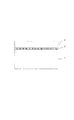
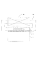
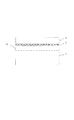
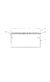
- 基板(1)からフィルム(1’)を引き離すために前記基板(1)をへき開する方法であって、以下の連続的なステップ、即ち、
(i)局部的に基板(1)の面に結合され、熱処理の作用下で基板(1)の面と平行な平面内で膨脹又は収縮するように設計された応力発生構造体(2)と呼ばれるものを形成するステップと、
(ii)膨張又は収縮を引き起こすように設計された前記構造体(2)に熱処理を適用し、基板(1)中に複数の局部応力を生じさせ、応力の組合せが引き離すフィルム(1’)を画定する基板の面と平行なへき開面(C)での基板の機械的強さより大きい応力を生じさせ、前記応力が前記平面(C)にわたって基板(1)のへき開をもたらすステップと、
を含む方法。 - 前記応力発生構造体(2)が、そのセル(2’)の壁(2”)が基板の面に垂直であるセル構造体であり、前記熱処理の作用下で前記壁を変形させるように設計された異なる熱膨張係数を有する少なくとも2種の材料(2a、2b)で構成されることを特徴とする、請求項1に記載の方法。
- セル(2’)の壁(2”)が、少なくとも2の比率だけ異なる熱膨張係数を有する、第1及び第2の材料(2a、2b)から形成された二材料ストリップであることを特徴とする、請求項2に記載の方法。
- 応力発生構造体が、以下の材料の組、Si/Ag、Si/Al、Si/Cu、Si/SiO2、Ge/Ag、Ge/Al、Ge/Cu、Ge/Fe、Ge/SiO2、サファイア/Ag、サファイア/Al、サファイア/Cu及び/又はサファイア/SiO2から形成された二材料ストリップを含むことを特徴とする、請求項3に記載の方法。
- セル(2’)の壁(2”)が第1及び第2の材料(2a、2b)から形成された二材料ストリップであり、一方が正の熱膨張係数を有し、他方が負の熱膨張係数を有することを特徴とする、請求項2に記載の方法。
- 二材料ストリップが以下の材料の組、Si/ZrW2O8、Cu/ZrW2O8、Al/ZrW2O8及び/又はAg/ZrW2O8から形成されることを特徴とする、請求項5に記載の方法。
- 二材料ストリップの、第1及び第2の材料が空隙によって又は第3の材料のストリップによって隔てられ、特に二材料ストリップがAg/ZrW2O8対によって形成され、第3の材料のストリップがシリコンであることを特徴とする、請求項3〜6のいずれか一項に記載の方法。
- 熱処理が20〜500℃の間の温度で適用されることを特徴とする、請求項1〜7のいずれか一項に記載の方法。
- 応力発生構造体(2)が、磁界の作用下で膨張又は収縮するようにさらに設計されていることを特徴とする、請求項1に記載の方法。
- 前記応力発生構造体(2)が、そのセル(2’)の壁(2”)が基板の面に垂直であるセル構造体であり、前記熱処理の作用下で前記壁を変形させるように設計された異なる熱膨張係数を有する少なくとも2種の材料(2a、2b)で構成されること及び前記材料の一方が磁気歪み材料であることを特徴とする、請求項9に記載の方法。
- 磁気歪み材料が、ターフェノールD、SmFe2、DyFe2又はTbFe2などの希土類/鉄合金であること、及び、他方の材料がシリコン、SiC又はゲルマニウムであることを特徴とする、請求項10に記載の方法。
- 熱処理が磁気歪み材料のキュリー温度未満の温度で適用されること、及び、磁界も前記磁気歪み材料を伸ばす又は縮めるために適切な前記構造体に印加されることを特徴とする、請求項10又は11に記載の方法。
- 基板(1)が細長い形状を有すること、及び、印加磁界が静的であり、基板(1)の最大寸法に平行に向けられることを特徴とする、請求項12に記載の方法。
- 基板(1)が円板の形態であること、及び印加磁界が回転磁界であることを特徴とする、請求項12に記載の方法。
- 応力発生構造体(2)が結合層(3)によって基板(1)の面に結合されていることを特徴とする、請求項1〜14のいずれか一項に記載の方法。
- 応力発生構造体(2)が、基板(1)の面に結合される前に、第1の材料(2a)の層のトレンチをエッチングすること、前記トレンチを第2の材料(2b)で充填すること、二材料ストリップを形成するように意図される第1の材料(2a)の層の部分をマスキングすること、及び第1の材料(2a)のマスクされていない部分を除去するように選択的に前記層をエッチングすることによって製作されることを特徴とする、請求項2〜15のいずれか一項に記載の方法。
- 応力発生構造体(2)が、第1の材料(2a)の層を基板(1)の面に堆積させることによって基板(1)に結合され、続いて前記層中のトレンチをエッチングし、第2の材料(2b)で前記トレンチを充填し、二材料ストリップを形成するように意図される第1の材料(2a)の層の部分をマスキングし、第1の材料(2a)のマスクされていない部分を除去するために前記層を選択的エッチングすることを特徴とする、請求項2〜15のいずれか一項に記載の方法。
- 基板(1)から引き離すフィルム(1’)の厚さが1〜100ミクロンの間、好ましくは30〜70ミクロンの間、例えば約50ミクロンであることを特徴とする、請求項1〜17のいずれか一項に記載の方法。
- 引き離すフィルム(1’)の厚さと応力発生構造体(2)の厚さとの比率が0.1〜10の間であることを特徴とする、請求項1〜18のいずれか一項に記載の方法。
- ステップ(ii)の前に、弱いゾーン(10)が前記弱いゾーン(10)にわたってへき開を引き起こすように基板(1)中に形成されることを特徴とする、請求項1〜19のいずれか一項に記載の方法。
- 前記弱いゾーン(10)が、5×10¹⁵〜1016原子/cm2の間の線量を用いるへき開面(C)の深さでの基板へのイオン注入によって形成されることを特徴とする、請求項20に記載の方法。
- 基板(1)及び引き離すフィルム(1’)がシリコンで製造されていること、及び、弱いゾーン(10)がSixGe1−x[式中、0<x<0.8]の層であり、ゲルマニウムの割合が界面での最小値から中心での最大値の間で徐々に変化することを特徴とする、請求項20に記載の方法。
- ステップ(ii)の前に、破砕イニシエータ(11)がへき開面(C)の深さで基板(1)中に生成されることを特徴とする、請求項1〜19のいずれか一項に記載の方法。
- ステップ(i)の前に、オプトエレクトロニクス及び/又は光起電力及び/又は電力用途及び/又は電子回路及び/又はマイクロシステム用である電子デバイスが、基板(1)から引き離すフィルム(1’)中又は上に形成されることを特徴とする、請求項1〜23のいずれか一項に記載の方法。
- フィルム(1’)が基板(1)から引き離された後、応力発生構造体(2)がフィルム(1’)から除去されることを特徴とする、請求項1〜24のいずれか一項に記載の方法。
- 基板をへき開するために再び応力発生構造体(2)を使用する目的で、引き離すフィルム(1’)から応力発生構造体(2)を除去した後、応力発生構造体(2)が再使用されることを特徴とする、請求項25に記載の方法。
- 基板(1)が半導体材料で製造されていることを特徴とする、請求項1〜26のいずれか一項に記載の方法。
- 基板(1)がインゴットであること、及びステップ(i)及び(ii)が、前記基板(1)から連続的に複数のフィルム(1’)を引き離すために数回適用されることを特徴とする、請求項1〜27のいずれか一項に記載の方法。
- 基板(1)及び前記基板(1)の面に結合された応力発生構造体(2)を含む集合体であって、前記応力発生構造体(2)が、そのセル(2’)の壁(2”)が基板(1)の面に垂直であるセル構造体であり、熱処理の作用下で前記壁を変形させるのに適切な異なる熱膨張係数を有する少なくとも2種の材料(2a、2b)で構成されることを特徴とする集合体。
- 光起電力、オプトエレクトロニクス又は電子工学の用途のための半導体デバイスであって、半導体材料のフィルム(1’)、及び前記フィルムの面に結合したセル構造体である支持体(2)を含み、そのセル(2’)の壁(2”)がフィルム(1’)の面に垂直であり、前記壁を熱処理の作用下で変形させるのに適切な相異なる熱膨張係数を有する少なくとも2種の材料(2a、2b)で構成される半導体デバイス。
Applications Claiming Priority (2)
| Application Number | Priority Date | Filing Date | Title |
|---|---|---|---|
| FR1061052 | 2010-12-22 | ||
| FR1061052A FR2969664B1 (fr) | 2010-12-22 | 2010-12-22 | Procede de clivage d'un substrat |
Publications (2)
| Publication Number | Publication Date |
|---|---|
| JP2012134459A true JP2012134459A (ja) | 2012-07-12 |
| JP5458362B2 JP5458362B2 (ja) | 2014-04-02 |
Family
ID=43927597
Family Applications (1)
| Application Number | Title | Priority Date | Filing Date |
|---|---|---|---|
| JP2011241537A Active JP5458362B2 (ja) | 2010-12-22 | 2011-11-02 | 基板をへき開する方法 |
Country Status (8)
| Country | Link |
|---|---|
| US (1) | US8420506B2 (ja) |
| EP (1) | EP2468931B1 (ja) |
| JP (1) | JP5458362B2 (ja) |
| KR (1) | KR101401580B1 (ja) |
| CN (1) | CN102543678B (ja) |
| FR (1) | FR2969664B1 (ja) |
| SG (1) | SG182051A1 (ja) |
| TW (1) | TW201230181A (ja) |
Cited By (2)
| Publication number | Priority date | Publication date | Assignee | Title |
|---|---|---|---|---|
| KR101372395B1 (ko) * | 2013-01-09 | 2014-03-10 | 한국과학기술원 | 나노제너레이터 분리 방법 및 이를 이용한 플렉서블 나노제너레이터 제조방법 |
| KR101547057B1 (ko) | 2014-02-12 | 2015-08-24 | 한국과학기술원 | 버퍼층을 이용한 나노제너레이터 분리 방법 및 이를 이용한 플렉서블 나노제너레이터 제조방법 |
Families Citing this family (11)
| Publication number | Priority date | Publication date | Assignee | Title |
|---|---|---|---|---|
| US20120217622A1 (en) * | 2010-05-21 | 2012-08-30 | International Business Machines Corporation | Method for Imparting a Controlled Amount of Stress in Semiconductor Devices for Fabricating Thin Flexible Circuits |
| FR2978600B1 (fr) | 2011-07-25 | 2014-02-07 | Soitec Silicon On Insulator | Procede et dispositif de fabrication de couche de materiau semi-conducteur |
| US8709957B2 (en) * | 2012-05-25 | 2014-04-29 | International Business Machines Corporation | Spalling utilizing stressor layer portions |
| FR3007892B1 (fr) * | 2013-06-27 | 2015-07-31 | Commissariat Energie Atomique | Procede de transfert d'une couche mince avec apport d'energie thermique a une zone fragilisee via une couche inductive |
| JP6182661B2 (ja) * | 2014-02-18 | 2017-08-16 | 日本碍子株式会社 | 半導体用複合基板のハンドル基板および半導体用複合基板 |
| JP6396852B2 (ja) * | 2015-06-02 | 2018-09-26 | 信越化学工業株式会社 | 酸化物単結晶薄膜を備えた複合ウェーハの製造方法 |
| CN107230611A (zh) * | 2016-03-25 | 2017-10-03 | 松下知识产权经营株式会社 | Iii族氮化物结晶制造方法以及ramo4基板 |
| CN107785244A (zh) * | 2017-09-27 | 2018-03-09 | 厦门三安光电有限公司 | 一种半导体外延生长方法及其石墨承载盘 |
| JP7373267B2 (ja) * | 2018-03-29 | 2023-11-02 | リンテック株式会社 | 個片体の製造方法 |
| CN109554668A (zh) * | 2018-12-17 | 2019-04-02 | 合肥鑫晟光电科技有限公司 | 坩埚喷嘴结构、坩埚以及清理喷嘴的方法 |
| CN114639635B (zh) * | 2022-03-17 | 2023-03-21 | 电子科技大学 | 一种单晶薄膜的剥离方法、单晶薄膜以及电子元器件 |
Citations (1)
| Publication number | Priority date | Publication date | Assignee | Title |
|---|---|---|---|---|
| US20070249140A1 (en) * | 2006-04-19 | 2007-10-25 | Interuniversitair Microelecktronica Centrum (Imec) | Method for the production of thin substrates |
Family Cites Families (11)
| Publication number | Priority date | Publication date | Assignee | Title |
|---|---|---|---|---|
| FR2681472B1 (fr) | 1991-09-18 | 1993-10-29 | Commissariat Energie Atomique | Procede de fabrication de films minces de materiau semiconducteur. |
| ATE261612T1 (de) * | 1996-12-18 | 2004-03-15 | Canon Kk | Vefahren zum herstellen eines halbleiterartikels unter verwendung eines substrates mit einer porösen halbleiterschicht |
| KR100529742B1 (ko) | 2000-08-01 | 2005-11-17 | 존 울프 인터내셔날 인코포레이티드 | 기판상의 박막 제조 방법 |
| US7176528B2 (en) * | 2003-02-18 | 2007-02-13 | Corning Incorporated | Glass-based SOI structures |
| JP2006024782A (ja) | 2004-07-08 | 2006-01-26 | Sharp Corp | 基板製造方法、および基板製造装置 |
| TW200703462A (en) * | 2005-04-13 | 2007-01-16 | Univ California | Wafer separation technique for the fabrication of free-standing (Al, In, Ga)N wafers |
| JP5064692B2 (ja) * | 2006-02-09 | 2012-10-31 | 信越化学工業株式会社 | Soi基板の製造方法 |
| US9362439B2 (en) | 2008-05-07 | 2016-06-07 | Silicon Genesis Corporation | Layer transfer of films utilizing controlled shear region |
| US8703521B2 (en) | 2009-06-09 | 2014-04-22 | International Business Machines Corporation | Multijunction photovoltaic cell fabrication |
| US20100310775A1 (en) | 2009-06-09 | 2010-12-09 | International Business Machines Corporation | Spalling for a Semiconductor Substrate |
| US20110048517A1 (en) | 2009-06-09 | 2011-03-03 | International Business Machines Corporation | Multijunction Photovoltaic Cell Fabrication |
-
2010
- 2010-12-22 FR FR1061052A patent/FR2969664B1/fr not_active Expired - Fee Related
-
2011
- 2011-11-02 JP JP2011241537A patent/JP5458362B2/ja active Active
- 2011-11-18 SG SG2011085628A patent/SG182051A1/en unknown
- 2011-11-23 TW TW100142965A patent/TW201230181A/zh unknown
- 2011-11-29 US US13/306,591 patent/US8420506B2/en active Active
- 2011-12-05 KR KR1020110129054A patent/KR101401580B1/ko active IP Right Grant
- 2011-12-21 CN CN201110433265.7A patent/CN102543678B/zh active Active
- 2011-12-22 EP EP11195129.9A patent/EP2468931B1/fr active Active
Patent Citations (1)
| Publication number | Priority date | Publication date | Assignee | Title |
|---|---|---|---|---|
| US20070249140A1 (en) * | 2006-04-19 | 2007-10-25 | Interuniversitair Microelecktronica Centrum (Imec) | Method for the production of thin substrates |
Cited By (2)
| Publication number | Priority date | Publication date | Assignee | Title |
|---|---|---|---|---|
| KR101372395B1 (ko) * | 2013-01-09 | 2014-03-10 | 한국과학기술원 | 나노제너레이터 분리 방법 및 이를 이용한 플렉서블 나노제너레이터 제조방법 |
| KR101547057B1 (ko) | 2014-02-12 | 2015-08-24 | 한국과학기술원 | 버퍼층을 이용한 나노제너레이터 분리 방법 및 이를 이용한 플렉서블 나노제너레이터 제조방법 |
Also Published As
| Publication number | Publication date |
|---|---|
| US8420506B2 (en) | 2013-04-16 |
| FR2969664B1 (fr) | 2013-06-14 |
| JP5458362B2 (ja) | 2014-04-02 |
| FR2969664A1 (fr) | 2012-06-29 |
| CN102543678A (zh) | 2012-07-04 |
| US20120161291A1 (en) | 2012-06-28 |
| EP2468931B1 (fr) | 2013-07-10 |
| EP2468931A1 (fr) | 2012-06-27 |
| KR101401580B1 (ko) | 2014-06-02 |
| KR20120071322A (ko) | 2012-07-02 |
| TW201230181A (en) | 2012-07-16 |
| CN102543678B (zh) | 2014-10-29 |
| SG182051A1 (en) | 2012-07-30 |
Similar Documents
| Publication | Publication Date | Title |
|---|---|---|
| JP5458362B2 (ja) | 基板をへき開する方法 | |
| US20170358704A1 (en) | Techniques for forming optoelectronic devices | |
| JP5031364B2 (ja) | エピタキシャル成長層の形成方法 | |
| JP5567569B2 (ja) | 選択した格子定数または制御した格子定数を有する半導体材料の層を使用する半導体構造または半導体デバイスを製造する方法 | |
| JP5031365B2 (ja) | エピタキシャル成長層の形成方法 | |
| JP5296281B2 (ja) | 脆弱化された基板およびそのような基板の製造方法 | |
| US7341927B2 (en) | Wafer bonded epitaxial templates for silicon heterostructures | |
| US6964914B2 (en) | Method of manufacturing a free-standing substrate made of monocrystalline semi-conductor material | |
| US10186630B2 (en) | Seed wafer for GaN thickening using gas- or liquid-phase epitaxy | |
| US20060035440A1 (en) | Method for manufacturing a free-standing substrate made of monocrystalline semiconductor material | |
| JP2009267427A (ja) | 制御された機械的保持力を有する剥離可能な基板、およびその製造方法 | |
| TW201448262A (zh) | 用於形成光電子裝置之技術 | |
| US20060091400A1 (en) | Composite structure with high heat dissipation | |
| US20200321242A1 (en) | Method of separating a film from a brittle material | |
| JP2005101630A (ja) | 半導体部材の製造方法 | |
| WO2010147081A1 (ja) | Ge膜付きSOI基板の製造方法及びGe膜付きSOI基板 | |
| KR20140060688A (ko) | 박막 접합 기판 제조방법 |
Legal Events
| Date | Code | Title | Description |
|---|---|---|---|
| A131 | Notification of reasons for refusal |
Free format text: JAPANESE INTERMEDIATE CODE: A131 Effective date: 20130820 |
|
| A521 | Request for written amendment filed |
Free format text: JAPANESE INTERMEDIATE CODE: A523 Effective date: 20131118 |
|
| TRDD | Decision of grant or rejection written | ||
| A01 | Written decision to grant a patent or to grant a registration (utility model) |
Free format text: JAPANESE INTERMEDIATE CODE: A01 Effective date: 20131217 |
|
| A61 | First payment of annual fees (during grant procedure) |
Free format text: JAPANESE INTERMEDIATE CODE: A61 Effective date: 20131224 |
|
| R150 | Certificate of patent or registration of utility model |
Ref document number: 5458362 Country of ref document: JP Free format text: JAPANESE INTERMEDIATE CODE: R150 Free format text: JAPANESE INTERMEDIATE CODE: R150 |
|
| R250 | Receipt of annual fees |
Free format text: JAPANESE INTERMEDIATE CODE: R250 |
|
| R250 | Receipt of annual fees |
Free format text: JAPANESE INTERMEDIATE CODE: R250 |
|
| R250 | Receipt of annual fees |
Free format text: JAPANESE INTERMEDIATE CODE: R250 |
|
| R250 | Receipt of annual fees |
Free format text: JAPANESE INTERMEDIATE CODE: R250 |
|
| R250 | Receipt of annual fees |
Free format text: JAPANESE INTERMEDIATE CODE: R250 |
|
| R250 | Receipt of annual fees |
Free format text: JAPANESE INTERMEDIATE CODE: R250 |
|
| R250 | Receipt of annual fees |
Free format text: JAPANESE INTERMEDIATE CODE: R250 |
|
| R250 | Receipt of annual fees |
Free format text: JAPANESE INTERMEDIATE CODE: R250 |