JP2012134459A - Method for cleaving substrate - Google Patents
Method for cleaving substrate Download PDFInfo
- Publication number
- JP2012134459A JP2012134459A JP2011241537A JP2011241537A JP2012134459A JP 2012134459 A JP2012134459 A JP 2012134459A JP 2011241537 A JP2011241537 A JP 2011241537A JP 2011241537 A JP2011241537 A JP 2011241537A JP 2012134459 A JP2012134459 A JP 2012134459A
- Authority
- JP
- Japan
- Prior art keywords
- substrate
- film
- stress
- stress generating
- generating structure
- Prior art date
- Legal status (The legal status is an assumption and is not a legal conclusion. Google has not performed a legal analysis and makes no representation as to the accuracy of the status listed.)
- Granted
Links
- 239000000758 substrate Substances 0.000 title claims abstract description 194
- 238000000034 method Methods 0.000 title claims abstract description 62
- 238000010438 heat treatment Methods 0.000 claims abstract description 32
- 238000003776 cleavage reaction Methods 0.000 claims abstract description 31
- 230000007017 scission Effects 0.000 claims abstract description 31
- 230000009471 action Effects 0.000 claims abstract description 23
- 239000000463 material Substances 0.000 claims description 183
- 229910052710 silicon Inorganic materials 0.000 claims description 48
- XUIMIQQOPSSXEZ-UHFFFAOYSA-N Silicon Chemical compound [Si] XUIMIQQOPSSXEZ-UHFFFAOYSA-N 0.000 claims description 42
- 239000010703 silicon Substances 0.000 claims description 42
- 239000004065 semiconductor Substances 0.000 claims description 13
- 229910052709 silver Inorganic materials 0.000 claims description 13
- 229910052732 germanium Inorganic materials 0.000 claims description 12
- 238000005530 etching Methods 0.000 claims description 11
- 229910052782 aluminium Inorganic materials 0.000 claims description 9
- 229910052594 sapphire Inorganic materials 0.000 claims description 9
- 239000010980 sapphire Substances 0.000 claims description 9
- 229910004298 SiO 2 Inorganic materials 0.000 claims description 8
- GNPVGFCGXDBREM-UHFFFAOYSA-N germanium atom Chemical compound [Ge] GNPVGFCGXDBREM-UHFFFAOYSA-N 0.000 claims description 8
- 239000003999 initiator Substances 0.000 claims description 8
- 229910000640 Fe alloy Inorganic materials 0.000 claims description 5
- 229910052802 copper Inorganic materials 0.000 claims description 5
- 238000000151 deposition Methods 0.000 claims description 5
- 230000005693 optoelectronics Effects 0.000 claims description 5
- 229910052761 rare earth metal Inorganic materials 0.000 claims description 5
- 150000002910 rare earth metals Chemical group 0.000 claims description 5
- 230000008602 contraction Effects 0.000 claims description 4
- 238000005468 ion implantation Methods 0.000 claims description 4
- 230000000873 masking effect Effects 0.000 claims description 4
- 229910003465 moissanite Inorganic materials 0.000 claims description 4
- 230000008569 process Effects 0.000 claims description 4
- 229910010271 silicon carbide Inorganic materials 0.000 claims description 4
- HBMJWWWQQXIZIP-UHFFFAOYSA-N silicon carbide Chemical compound [Si+]#[C-] HBMJWWWQQXIZIP-UHFFFAOYSA-N 0.000 claims description 3
- 230000003068 static effect Effects 0.000 claims description 3
- 229910001329 Terfenol-D Inorganic materials 0.000 claims 1
- 230000035882 stress Effects 0.000 description 63
- 239000010410 layer Substances 0.000 description 54
- 210000004027 cell Anatomy 0.000 description 43
- BQCADISMDOOEFD-UHFFFAOYSA-N Silver Chemical compound [Ag] BQCADISMDOOEFD-UHFFFAOYSA-N 0.000 description 11
- 229910052751 metal Inorganic materials 0.000 description 11
- 239000002184 metal Substances 0.000 description 11
- 239000004332 silver Substances 0.000 description 11
- 239000000853 adhesive Substances 0.000 description 8
- 230000001070 adhesive effect Effects 0.000 description 8
- 230000008901 benefit Effects 0.000 description 7
- 210000002421 cell wall Anatomy 0.000 description 7
- PJWVRCBRZWEQHL-UHFFFAOYSA-N 2,3-bis(2-hydroxyphenyl)phenol Chemical compound OC1=CC=CC=C1C1=CC=CC(O)=C1C1=CC=CC=C1O PJWVRCBRZWEQHL-UHFFFAOYSA-N 0.000 description 5
- XAGFODPZIPBFFR-UHFFFAOYSA-N aluminium Chemical compound [Al] XAGFODPZIPBFFR-UHFFFAOYSA-N 0.000 description 5
- 239000010949 copper Substances 0.000 description 5
- 238000004519 manufacturing process Methods 0.000 description 5
- 230000006698 induction Effects 0.000 description 4
- XEEYBQQBJWHFJM-UHFFFAOYSA-N Iron Chemical compound [Fe] XEEYBQQBJWHFJM-UHFFFAOYSA-N 0.000 description 3
- 238000005229 chemical vapour deposition Methods 0.000 description 3
- 239000013078 crystal Substances 0.000 description 3
- 150000002500 ions Chemical class 0.000 description 3
- 238000005498 polishing Methods 0.000 description 3
- 239000000126 substance Substances 0.000 description 3
- VYPSYNLAJGMNEJ-UHFFFAOYSA-N Silicium dioxide Chemical compound O=[Si]=O VYPSYNLAJGMNEJ-UHFFFAOYSA-N 0.000 description 2
- 230000003321 amplification Effects 0.000 description 2
- YCIMNLLNPGFGHC-UHFFFAOYSA-N catechol Chemical compound OC1=CC=CC=C1O YCIMNLLNPGFGHC-UHFFFAOYSA-N 0.000 description 2
- 238000011109 contamination Methods 0.000 description 2
- 238000010586 diagram Methods 0.000 description 2
- 230000000694 effects Effects 0.000 description 2
- 229920006332 epoxy adhesive Polymers 0.000 description 2
- 150000002739 metals Chemical class 0.000 description 2
- 238000003199 nucleic acid amplification method Methods 0.000 description 2
- 239000011241 protective layer Substances 0.000 description 2
- 230000000717 retained effect Effects 0.000 description 2
- 238000000926 separation method Methods 0.000 description 2
- 229910052814 silicon oxide Inorganic materials 0.000 description 2
- 239000007787 solid Substances 0.000 description 2
- 238000004544 sputter deposition Methods 0.000 description 2
- 239000010936 titanium Substances 0.000 description 2
- 229910052719 titanium Inorganic materials 0.000 description 2
- RYGMFSIKBFXOCR-UHFFFAOYSA-N Copper Chemical compound [Cu] RYGMFSIKBFXOCR-UHFFFAOYSA-N 0.000 description 1
- 229910001218 Gallium arsenide Inorganic materials 0.000 description 1
- 229910052581 Si3N4 Inorganic materials 0.000 description 1
- RTAQQCXQSZGOHL-UHFFFAOYSA-N Titanium Chemical compound [Ti] RTAQQCXQSZGOHL-UHFFFAOYSA-N 0.000 description 1
- 239000000956 alloy Substances 0.000 description 1
- 238000000137 annealing Methods 0.000 description 1
- 239000012298 atmosphere Substances 0.000 description 1
- 230000015572 biosynthetic process Effects 0.000 description 1
- 230000001413 cellular effect Effects 0.000 description 1
- 210000003850 cellular structure Anatomy 0.000 description 1
- 238000003486 chemical etching Methods 0.000 description 1
- 239000003795 chemical substances by application Substances 0.000 description 1
- 239000002131 composite material Substances 0.000 description 1
- 230000008878 coupling Effects 0.000 description 1
- 238000010168 coupling process Methods 0.000 description 1
- 238000005859 coupling reaction Methods 0.000 description 1
- 230000008021 deposition Effects 0.000 description 1
- 230000001627 detrimental effect Effects 0.000 description 1
- OJLGWNFZMTVNCX-UHFFFAOYSA-N dioxido(dioxo)tungsten;zirconium(4+) Chemical compound [Zr+4].[O-][W]([O-])(=O)=O.[O-][W]([O-])(=O)=O OJLGWNFZMTVNCX-UHFFFAOYSA-N 0.000 description 1
- 238000002848 electrochemical method Methods 0.000 description 1
- 238000005516 engineering process Methods 0.000 description 1
- 230000008020 evaporation Effects 0.000 description 1
- 238000001704 evaporation Methods 0.000 description 1
- 239000007943 implant Substances 0.000 description 1
- 229910052742 iron Inorganic materials 0.000 description 1
- 230000001788 irregular Effects 0.000 description 1
- 238000012067 mathematical method Methods 0.000 description 1
- 230000007246 mechanism Effects 0.000 description 1
- 238000005457 optimization Methods 0.000 description 1
- 230000003647 oxidation Effects 0.000 description 1
- 238000007254 oxidation reaction Methods 0.000 description 1
- 230000003071 parasitic effect Effects 0.000 description 1
- 238000009832 plasma treatment Methods 0.000 description 1
- 239000011148 porous material Substances 0.000 description 1
- 230000001737 promoting effect Effects 0.000 description 1
- 230000001681 protective effect Effects 0.000 description 1
- 229910002059 quaternary alloy Inorganic materials 0.000 description 1
- HQVNEWCFYHHQES-UHFFFAOYSA-N silicon nitride Chemical compound N12[Si]34N5[Si]62N3[Si]51N64 HQVNEWCFYHHQES-UHFFFAOYSA-N 0.000 description 1
- 238000005476 soldering Methods 0.000 description 1
- 238000003756 stirring Methods 0.000 description 1
- 230000008646 thermal stress Effects 0.000 description 1
- 230000007704 transition Effects 0.000 description 1
- 238000011282 treatment Methods 0.000 description 1
- XLYOFNOQVPJJNP-UHFFFAOYSA-N water Chemical compound O XLYOFNOQVPJJNP-UHFFFAOYSA-N 0.000 description 1
Images


Classifications
-
- H—ELECTRICITY
- H01—ELECTRIC ELEMENTS
- H01L—SEMICONDUCTOR DEVICES NOT COVERED BY CLASS H10
- H01L21/00—Processes or apparatus adapted for the manufacture or treatment of semiconductor or solid state devices or of parts thereof
- H01L21/02—Manufacture or treatment of semiconductor devices or of parts thereof
- H01L21/04—Manufacture or treatment of semiconductor devices or of parts thereof the devices having at least one potential-jump barrier or surface barrier, e.g. PN junction, depletion layer or carrier concentration layer
- H01L21/18—Manufacture or treatment of semiconductor devices or of parts thereof the devices having at least one potential-jump barrier or surface barrier, e.g. PN junction, depletion layer or carrier concentration layer the devices having semiconductor bodies comprising elements of Group IV of the Periodic System or AIIIBV compounds with or without impurities, e.g. doping materials
- H01L21/30—Treatment of semiconductor bodies using processes or apparatus not provided for in groups H01L21/20 - H01L21/26
-
- C—CHEMISTRY; METALLURGY
- C30—CRYSTAL GROWTH
- C30B—SINGLE-CRYSTAL GROWTH; UNIDIRECTIONAL SOLIDIFICATION OF EUTECTIC MATERIAL OR UNIDIRECTIONAL DEMIXING OF EUTECTOID MATERIAL; REFINING BY ZONE-MELTING OF MATERIAL; PRODUCTION OF A HOMOGENEOUS POLYCRYSTALLINE MATERIAL WITH DEFINED STRUCTURE; SINGLE CRYSTALS OR HOMOGENEOUS POLYCRYSTALLINE MATERIAL WITH DEFINED STRUCTURE; AFTER-TREATMENT OF SINGLE CRYSTALS OR A HOMOGENEOUS POLYCRYSTALLINE MATERIAL WITH DEFINED STRUCTURE; APPARATUS THEREFOR
- C30B33/00—After-treatment of single crystals or homogeneous polycrystalline material with defined structure
- C30B33/06—Joining of crystals
-
- C—CHEMISTRY; METALLURGY
- C30—CRYSTAL GROWTH
- C30B—SINGLE-CRYSTAL GROWTH; UNIDIRECTIONAL SOLIDIFICATION OF EUTECTIC MATERIAL OR UNIDIRECTIONAL DEMIXING OF EUTECTOID MATERIAL; REFINING BY ZONE-MELTING OF MATERIAL; PRODUCTION OF A HOMOGENEOUS POLYCRYSTALLINE MATERIAL WITH DEFINED STRUCTURE; SINGLE CRYSTALS OR HOMOGENEOUS POLYCRYSTALLINE MATERIAL WITH DEFINED STRUCTURE; AFTER-TREATMENT OF SINGLE CRYSTALS OR A HOMOGENEOUS POLYCRYSTALLINE MATERIAL WITH DEFINED STRUCTURE; APPARATUS THEREFOR
- C30B29/00—Single crystals or homogeneous polycrystalline material with defined structure characterised by the material or by their shape
- C30B29/02—Elements
- C30B29/06—Silicon
-
- H—ELECTRICITY
- H01—ELECTRIC ELEMENTS
- H01L—SEMICONDUCTOR DEVICES NOT COVERED BY CLASS H10
- H01L21/00—Processes or apparatus adapted for the manufacture or treatment of semiconductor or solid state devices or of parts thereof
- H01L21/02—Manufacture or treatment of semiconductor devices or of parts thereof
- H01L21/04—Manufacture or treatment of semiconductor devices or of parts thereof the devices having at least one potential-jump barrier or surface barrier, e.g. PN junction, depletion layer or carrier concentration layer
- H01L21/18—Manufacture or treatment of semiconductor devices or of parts thereof the devices having at least one potential-jump barrier or surface barrier, e.g. PN junction, depletion layer or carrier concentration layer the devices having semiconductor bodies comprising elements of Group IV of the Periodic System or AIIIBV compounds with or without impurities, e.g. doping materials
- H01L21/185—Joining of semiconductor bodies for junction formation
- H01L21/187—Joining of semiconductor bodies for junction formation by direct bonding
-
- H—ELECTRICITY
- H01—ELECTRIC ELEMENTS
- H01L—SEMICONDUCTOR DEVICES NOT COVERED BY CLASS H10
- H01L21/00—Processes or apparatus adapted for the manufacture or treatment of semiconductor or solid state devices or of parts thereof
- H01L21/02—Manufacture or treatment of semiconductor devices or of parts thereof
- H01L21/04—Manufacture or treatment of semiconductor devices or of parts thereof the devices having at least one potential-jump barrier or surface barrier, e.g. PN junction, depletion layer or carrier concentration layer
- H01L21/18—Manufacture or treatment of semiconductor devices or of parts thereof the devices having at least one potential-jump barrier or surface barrier, e.g. PN junction, depletion layer or carrier concentration layer the devices having semiconductor bodies comprising elements of Group IV of the Periodic System or AIIIBV compounds with or without impurities, e.g. doping materials
- H01L21/20—Deposition of semiconductor materials on a substrate, e.g. epitaxial growth solid phase epitaxy
- H01L21/2003—Deposition of semiconductor materials on a substrate, e.g. epitaxial growth solid phase epitaxy characterised by the substrate
- H01L21/2007—Bonding of semiconductor wafers to insulating substrates or to semiconducting substrates using an intermediate insulating layer
-
- H—ELECTRICITY
- H01—ELECTRIC ELEMENTS
- H01L—SEMICONDUCTOR DEVICES NOT COVERED BY CLASS H10
- H01L21/00—Processes or apparatus adapted for the manufacture or treatment of semiconductor or solid state devices or of parts thereof
- H01L21/02—Manufacture or treatment of semiconductor devices or of parts thereof
- H01L21/04—Manufacture or treatment of semiconductor devices or of parts thereof the devices having at least one potential-jump barrier or surface barrier, e.g. PN junction, depletion layer or carrier concentration layer
- H01L21/18—Manufacture or treatment of semiconductor devices or of parts thereof the devices having at least one potential-jump barrier or surface barrier, e.g. PN junction, depletion layer or carrier concentration layer the devices having semiconductor bodies comprising elements of Group IV of the Periodic System or AIIIBV compounds with or without impurities, e.g. doping materials
- H01L21/30—Treatment of semiconductor bodies using processes or apparatus not provided for in groups H01L21/20 - H01L21/26
- H01L21/302—Treatment of semiconductor bodies using processes or apparatus not provided for in groups H01L21/20 - H01L21/26 to change their surface-physical characteristics or shape, e.g. etching, polishing, cutting
- H01L21/304—Mechanical treatment, e.g. grinding, polishing, cutting
-
- H—ELECTRICITY
- H01—ELECTRIC ELEMENTS
- H01L—SEMICONDUCTOR DEVICES NOT COVERED BY CLASS H10
- H01L21/00—Processes or apparatus adapted for the manufacture or treatment of semiconductor or solid state devices or of parts thereof
- H01L21/70—Manufacture or treatment of devices consisting of a plurality of solid state components formed in or on a common substrate or of parts thereof; Manufacture of integrated circuit devices or of parts thereof
- H01L21/71—Manufacture of specific parts of devices defined in group H01L21/70
- H01L21/76—Making of isolation regions between components
- H01L21/762—Dielectric regions, e.g. EPIC dielectric isolation, LOCOS; Trench refilling techniques, SOI technology, use of channel stoppers
- H01L21/7624—Dielectric regions, e.g. EPIC dielectric isolation, LOCOS; Trench refilling techniques, SOI technology, use of channel stoppers using semiconductor on insulator [SOI] technology
- H01L21/76251—Dielectric regions, e.g. EPIC dielectric isolation, LOCOS; Trench refilling techniques, SOI technology, use of channel stoppers using semiconductor on insulator [SOI] technology using bonding techniques
- H01L21/76254—Dielectric regions, e.g. EPIC dielectric isolation, LOCOS; Trench refilling techniques, SOI technology, use of channel stoppers using semiconductor on insulator [SOI] technology using bonding techniques with separation/delamination along an ion implanted layer, e.g. Smart-cut, Unibond
Abstract
Description
本発明は、基板からフィルムを引き離す目的で前記基板をへき開する方法に関する。 The present invention relates to a method of cleaving the substrate for the purpose of pulling the film away from the substrate.
基板からの厚膜の引き離しは、特に半導体工業において実施されている。 The separation of the thick film from the substrate is carried out particularly in the semiconductor industry.
様々な引き離し法が既に知られ広く使用されている。 Various separation methods are already known and widely used.
ある方法は、引き離すフィルムを画定する脆化ゾーンを基板内に形成し、続いて脆化ゾーンで基板がへき開するように、基板又は脆化ゾーンに応力を印加するステップを含む。これらの応力は熱を元にしても及び/又は機械的な起点などによってもよい。 One method includes forming an embrittlement zone in the substrate that defines a film to be detached, followed by applying stress to the substrate or the embrittlement zone such that the substrate is cleaved in the embrittlement zone. These stresses may be based on heat and / or mechanical origins.
したがって、スマートカット(SmartCut)(登録商標)法は、ドナー基板に原子種を注入することによって脆化ゾーンを形成して、移動させるフィルムを画定し、続いて、レシーバ基板にドナー基板を結合させ、脆化ゾーンでドナー基板をへき開し、結果としてフィルムをレシーバ基板上に移動させるステップを含む。 Therefore, the SmartCut (R) method forms an embrittlement zone by injecting atomic species into the donor substrate to define the film to be moved, and subsequently bonds the donor substrate to the receiver substrate. Cleaving the donor substrate in the embrittlement zone and consequently moving the film onto the receiver substrate.
しかし、この方法は、薄い、すなわち、通常1ミクロン未満の厚さを有するフィルムを移動させるのにより適切である。 However, this method is more appropriate for moving films that are thin, i.e., typically having a thickness of less than 1 micron.
工業用注入機は最大200keVのエネルギーを現在有し、それによって、材料及び注入されるイオン種に依存して、最大約2ミクロン注入深さを達成することもある。 Industrial implanters currently have an energy of up to 200 keV, thereby achieving up to about 2 micron implant depth, depending on the material and ion species being implanted.
例えば、シリコンへH+イオンを注入することによって、約1.8ミクロンの深さを達成することは可能である。しかし、より高密度のGaNにおいては、達成される深さはより小さい。 For example, it is possible to achieve a depth of about 1.8 microns by implanting H + ions into silicon. However, for higher density GaN, the depth achieved is smaller.
高エネルギーの注入機(すなわち、約1MeVで運転する)によって、最大20ミクロンの深さを達成することは可能になるであろうが、しかし、この方法は、これらの装置が高コストであるために経済的に実現可能ではない。 High energy injectors (ie, operating at about 1 MeV) will be able to achieve depths of up to 20 microns, but this method is costly for these devices. Is not economically feasible.
米国特許出願公開第2007/0249140号は、金属層、特に銀及び/又はアルミニウムペーストがシリコン基板面に堆積された、基板から層を引き離す方法について述べている。 U.S. Patent Application Publication No. 2007/0249140 describes a method of separating a layer from a substrate, in which a metal layer, in particular silver and / or aluminum paste, is deposited on the silicon substrate surface.
金属層で覆われた基板に熱応力を印加することによって、引き離すように意図される層の厚さに対応する深さに基板中にへき開応力を生じさせ、結果として基板のへき開及び所望の層の引き離しが得られる。 Application of thermal stress to the substrate covered with the metal layer causes cleavage stress in the substrate to a depth corresponding to the thickness of the layer intended to be pulled apart, resulting in cleavage of the substrate and the desired layer. Can be separated.
得られるへき開応力は、金属層材料と基板材料との間の熱膨張係数(TEC)の差に依存する。 The resulting cleavage stress depends on the difference in coefficient of thermal expansion (TEC) between the metal layer material and the substrate material.
したがって、例えば、シリコンの熱膨張係数は4.6×10⁻⁶K−1であるが、銀の熱膨張係数は20×10−6K−1であり、アルミニウムの熱膨張係数は24×10−6K−1である。 Thus, for example, the thermal expansion coefficient of silicon is 4.6 × 10 −6 K −1 , while the thermal expansion coefficient of silver is 20 × 10 −6 K −1 and the thermal expansion coefficient of aluminum is 24 × 10 6. -6K- 1 .
しかしながら、シリコン基板に金属を堆積させることには、半導体層を汚染する危険性があり、この層から製作されるデバイスの動作にとって有害となろう。 However, depositing metal on a silicon substrate has the risk of contaminating the semiconductor layer and would be detrimental to the operation of devices made from this layer.
さらに、応力発生層の熱膨張係数は、使用される材料の性質に依存する。 Furthermore, the thermal expansion coefficient of the stress generating layer depends on the nature of the material used.
その結果、当業者は、この方法の定義の範囲内で市販の材料によって必然的に限定を受けている。 Consequently, those skilled in the art are necessarily limited by commercially available materials within the definition of this method.
特に、所望の熱膨張係数を有する応力発生層を必ずしも形成することができないことがある。 In particular, a stress generating layer having a desired thermal expansion coefficient may not always be formed.
最終的に、応力発生層を前述の方法に従って膨張させるためには、高温(すなわち、通常およそ800℃)に応力発生層を加熱することが一般に必要である。 Finally, it is generally necessary to heat the stress-generating layer to an elevated temperature (ie, typically around 800 ° C.) in order to expand the stress-generating layer according to the method described above.
しかし、この温度範囲のシリコンは展性があり、基板のへき開にとって不利である。 However, silicon in this temperature range is malleable and is disadvantageous for substrate cleavage.
したがって、本発明の一目的は、典型的には1〜100ミクロンの厚さを有するフィルムを基板から引き離し、上述の方法の欠点を回避する方法を提供することである。 Accordingly, it is an object of the present invention to provide a method of pulling a film, typically having a thickness of 1-100 microns, away from the substrate, avoiding the disadvantages of the methods described above.
より正確には、本発明の狙いは、基板の材料を汚染する危険性を伴わないで基板からフィルムを引き離すことを可能にすることである。 More precisely, the aim of the present invention is to allow the film to be pulled away from the substrate without the risk of contaminating the substrate material.
本発明の別の目的は、基板をへき開するために必要な温度を限定することである。 Another object of the invention is to limit the temperature required to cleave the substrate.
さらに、本発明はまた、特に最適に基板をへき開するため、応力発生構造体の熱膨張係数において選択のより大きい自由度を提供する必要がある。 Furthermore, the present invention also needs to provide greater freedom of choice in the coefficient of thermal expansion of the stress generating structure in order to cleave the substrate particularly optimally.
本発明によれば、基板からフィルムを引き離すために前記基板をへき開する方法であって、以下の連続的なステップ、即ち、
(i)局部的に基板の面に結合され、熱処理の作用下で基板の面と平行な平面内で膨脹又は収縮するように設計された応力発生構造体と呼ばれるものを形成するステップと、(ii)膨張又は収縮を引き起こすように設計された前記構造体に熱処理を適用し、基板中に複数の局部応力を生じさせ、応力の組合せが引き離すフィルムを画定する基板の面と平行なへき開面での基板の機械的強さより大きい応力を生じさせ、前記応力が前記平面にわたって基板のへき開をもたらすステップと、を含む方法が提案される。
In accordance with the present invention, a method of cleaving the substrate to pull the film away from the substrate, comprising the following sequential steps:
(I) forming a so-called stress generating structure that is locally bonded to the surface of the substrate and designed to expand or contract in a plane parallel to the surface of the substrate under the action of heat treatment; ii) applying a heat treatment to the structure designed to cause expansion or contraction, creating a plurality of local stresses in the substrate, with a cleavage plane parallel to the surface of the substrate defining the film from which the combination of stresses separates; Generating a stress greater than the mechanical strength of the substrate, the stress causing cleavage of the substrate across the plane.
本明細書において「結合した」という用語は、応力発生構造体と基板の面との間の凝集力が、界面での破壊がなく、構造体の変形により生じた応力が、基板をへき開するために基板に伝達されるように、構造体の膨脹又は収縮の間に働く応力より大きくなければならないことを意味するものと理解される。 In this specification, the term “bonded” means that the cohesive force between the stress generating structure and the surface of the substrate is not broken at the interface, and the stress generated by the deformation of the structure cleaves the substrate. It is understood that it must be greater than the stress acting during the expansion or contraction of the structure in order to be transmitted to the substrate.
「局部的に」という用語は、応力発生構造体と基板との間の結合が、基板の面の全地点ではなく基板の面の画定された領域にのみ存在することを意味するものと理解される。 The term “locally” is understood to mean that the bond between the stress generating structure and the substrate exists only in a defined area of the substrate surface, not at all points of the substrate surface. The
特に有利には、前記応力発生構造体はセル構造体であり、そのセルの壁は基板の面に垂直であり、異なる熱膨張係数を有する少なくとも2種の材料で構成され、前記壁を前記熱処理の作用下で変形させ、二材料ストリップ作用を与えるように設計されている。 Particularly preferably, the stress generating structure is a cell structure, the walls of the cell being perpendicular to the plane of the substrate and made of at least two materials having different coefficients of thermal expansion, the walls being subjected to the heat treatment. It is designed to be deformed under the action of and to give a bi-material strip action.
本明細書において「二材料ストリップ作用を与える」という表現は、異なる熱膨張係数を有する2種の材料が、熱処理の作用下で、及び材料の一方がまた磁歪性である場合、場合によって、磁界の作用下で、集合体が膨脹又は収縮することにより変形するように互いに結合されるように配置されることを意味するものと理解される。 In this specification, the expression “provides a bi-material strip action” means that two materials having different coefficients of thermal expansion are subject to magnetic field under the action of heat treatment and if one of the materials is also magnetostrictive. Under the action of, it is understood to mean that the assembly is arranged to be joined together so as to deform by expanding or contracting.
下記に述べられた実施形態によれば、2種の材料は、2種の材料間の界面が基板の面に実質的に垂直な面を有する、一緒に結合した2枚のストリップの形態をとってもよい。 According to the embodiments described below, the two materials may take the form of two strips joined together, with the interface between the two materials having a plane substantially perpendicular to the plane of the substrate. Good.
ひいては、「二材料ストリップ」という用語は、一緒に結合した複数のストリップの形態で、各材料間の界面が実質的に基板の面に垂直な面の形態である、異なる膨張係数を有する2種以上の材料の任意の配置を意味すると理解される。 Thus, the term “bi-material strip” refers to two types having different expansion coefficients in the form of a plurality of strips bonded together, the interface between each material being in the form of a plane that is substantially perpendicular to the plane of the substrate. It is understood to mean any arrangement of the above materials.
したがって、この定義は、例えばそれぞれ正のTECを有する材料のストリップ及び負のTECを有する材料のストリップに取り囲まれたシリコンの中央ストリップで構成される三材料ストリップを含む。 Thus, this definition includes, for example, a three-material strip composed of a strip of material each having a positive TEC and a central strip of silicon surrounded by a strip of material having a negative TEC.
本発明の一実施形態によれば、セルの壁は、少なくとも2の比率だけ異なる熱膨張係数を有する第1及び第2の材料から形成された二材料ストリップである。 According to one embodiment of the invention, the cell walls are bi-material strips formed from first and second materials having different coefficients of thermal expansion by a ratio of at least two.
例えば、応力発生構造体は、以下の材料の組、Si/Ag、Si/Al、Si/Cu、Si/SiO2、Ge/Ag、Ge/Al、Ge/Cu、Ge/Fe、Ge/SiO2、サファイア/Ag、サファイア/Al、サファイア/Cu及び/又はサファイア/SiO2から形成される二材料ストリップを含む。 For example, the stress generating structure may include the following material sets: Si / Ag, Si / Al, Si / Cu, Si / SiO 2 , Ge / Ag, Ge / Al, Ge / Cu, Ge / Fe, Ge / SiO 2 , comprising a bi-material strip formed from sapphire / Ag, sapphire / Al, sapphire / Cu and / or sapphire / SiO 2 .
別の実施形態によれば、セルの壁は、一方は正の熱膨張係数を有し、他方は負の熱膨張係数を有する第1及び第2の材料から形成された二材料ストリップである。 According to another embodiment, the cell walls are bi-material strips formed from first and second materials, one having a positive coefficient of thermal expansion and the other having a negative coefficient of thermal expansion.
例えば、前記二材料ストリップは、以下の材料の組、Si/ZrW2O8、Cu/ZrW2O8、Al/ZrW2O8及び/又はAg/ZrW2O8から形成される。 For example, the bi-material strip is formed from the following set of materials: Si / ZrW 2 O 8 , Cu / ZrW 2 O 8 , Al / ZrW 2 O 8 and / or Ag / ZrW 2 O 8 .
別の実施形態によれば、二材料ストリップの第1及び第2の材料は、空隙又は第3の材料のストリップによって隔てられ、特に、二材料ストリップはAg/ZrW2O8対によって形成され、第3の材料のストリップはシリコンである。 According to another embodiment, the first and second materials of the bi-material strip are separated by an air gap or a third material strip, in particular the bi-material strip is formed by an Ag / ZrW 2 O 8 pair, The strip of third material is silicon.
特に、有利に、ステップ(ii)の熱処理は20〜500℃の間の温度で適用される。 In particular, the heat treatment of step (ii) is preferably applied at a temperature between 20 and 500 ° C.
本発明の特に有利な一実施形態によれば、応力発生構造体は、磁界の作用下で基板の面と平行な平面内で膨脹又は収縮するようにさらに設計されている。 According to a particularly advantageous embodiment of the invention, the stress generating structure is further designed to expand or contract in a plane parallel to the plane of the substrate under the action of a magnetic field.
この目的のために、前記応力発生構造体はセル構造体であり、そのセルの壁は基板の面に垂直であり、相異なる熱膨張係数を有する少なくとも2種の材料で構成され、前記熱処理の作用下で前記壁を変形させるように設計され、前記材料の一方は磁気歪み材料である。 For this purpose, the stress generating structure is a cell structure, the cell walls are perpendicular to the plane of the substrate and are composed of at least two materials having different thermal expansion coefficients, Designed to deform the wall under action, one of the materials being a magnetostrictive material.
好ましくは、磁気歪み材料は、ターフェノールD(terfenol−D)、SmFe2、DyFe2又は、TbFe2などの希土類/鉄合金であり、他方の材料はシリコン、SiC又はゲルマニウムである。 Preferably, the magnetostrictive material is a rare earth / iron alloy such as terphenol D, SmFe 2 , DyFe 2 or TbFe 2 and the other material is silicon, SiC or germanium.
この場合、好ましくは、熱処理は磁気歪み材料のキュリー温度未満の温度で適用され、磁界も前記磁気歪み材料を伸ばす又は縮めるのに適切な前記応力発生構造体に印加される。 In this case, preferably a heat treatment is applied at a temperature below the Curie temperature of the magnetostrictive material and a magnetic field is also applied to the stress generating structure suitable for stretching or contracting the magnetostrictive material.
基板が細長い形状である場合、印加磁界は静的であることが好ましく、基板の最大寸法と平行に向けられる。 If the substrate has an elongated shape, the applied magnetic field is preferably static and is oriented parallel to the maximum dimension of the substrate.
基板が円板の形態をしている場合、印加磁界は、基板の面と平行な平面に垂直な2方向に構造体を膨張又は収縮させるような回転磁界である。 When the substrate is in the form of a disk, the applied magnetic field is a rotating magnetic field that expands or contracts the structure in two directions perpendicular to a plane parallel to the surface of the substrate.
本発明の特定の一実施形態によれば、応力発生構造体は、結合層によって基板の面に結合される。 According to one particular embodiment of the invention, the stress generating structure is bonded to the surface of the substrate by a bonding layer.
応力発生構造体は、基板に結合される前に、第1の材料の層にトレンチをエッチングすること、前記トレンチを第2の材料で充填すること、二材料ストリップを形成するように意図される第1の材料の層の部分をマスキングすること、及び第1の材料のマスクされていない部分を除去するように選択的に前記層をエッチングすることによって製作することができる。 The stress generating structure is intended to etch a trench in a layer of a first material, fill the trench with a second material, and form a bi-material strip before being bonded to a substrate. It can be fabricated by masking portions of the layer of first material and selectively etching the layer to remove unmasked portions of the first material.
代替として、応力発生構造体は、第1の材料の層を基板の面に堆積させることによって基板に結合され、続いて前記層中にトレンチをエッチングし、第2の材料で前記トレンチを充填し、二材料ストリップを形成するように意図される第1の材料の層の部分をマスキングし、第1の材料のマスクされていない部分を除去するために前記層を選択的エッチングする。 Alternatively, the stress generating structure is bonded to the substrate by depositing a layer of a first material on the surface of the substrate, followed by etching a trench in the layer and filling the trench with a second material. Masking a portion of the first material layer intended to form a bi-material strip and selectively etching the layer to remove the unmasked portion of the first material.
基板から引き離すフィルムの厚さは、1〜100ミクロンの間、好ましくは30〜70ミクロンの間で、例えば約50ミクロンである。 The thickness of the film pulled away from the substrate is between 1 and 100 microns, preferably between 30 and 70 microns, for example about 50 microns.
通常、引き離すフィルムの厚さと応力発生構造体の厚さとの比率は、0.1〜10の間にある。 Usually, the ratio of the thickness of the film to be separated and the thickness of the stress generating structure is between 0.1 and 10.
特定の一実施形態によれば、ステップ(ii)の前に、弱いゾーンは、前記弱いゾーンにわたってへき開を引き起こすように、基板中に形成される。 According to one particular embodiment, prior to step (ii), a weak zone is formed in the substrate to cause cleavage across the weak zone.
例えば、前記弱いゾーンは、5×10¹⁵及び1016原子/cm2の間の線量を用いるへき開面の深さでの基板へのイオン注入によって形成される。 For example, the weak zone is formed by ion implantation into the substrate at a cleavage plane depth using a dose between 5 × 10 15 and 10 16 atoms / cm 2 .
代替として、引き離す基板及びフィルムはシリコンで製造されており、弱いゾーンはSixGe1−x[式中、0<x<0.8]の層であり、ゲルマニウムの割合は界面での最小値から中央での最大値の間で徐々に変化する。 Alternatively, the separating substrate and film are made of silicon, the weak zone is a Si x Ge 1-x where 0 <x <0.8, and the germanium fraction is the minimum at the interface It gradually changes between the maximum value at the center.
一実施形態によれば、ステップ(ii)の前に、破砕イニシエータはへき開面の深さで基板中に生成される。 According to one embodiment, prior to step (ii), a crushing initiator is generated in the substrate at the depth of the cleavage plane.
ステップ(i)の前に、オプトエレクトロニクス及び/又は光起電力及び/又は電力用途及び/又は電子回路及び/又はマイクロシステム用である電子デバイスを、基板から引き離すフィルム中又は上に形成することができる。 Before step (i), an electronic device for optoelectronics and / or photovoltaic and / or power applications and / or electronic circuits and / or microsystems may be formed in or on the film that is pulled away from the substrate. it can.
フィルムが基板から引き離された後、応力発生構造体は、フィルムから除去されてもよい。 After the film is pulled away from the substrate, the stress generating structure may be removed from the film.
例えば、応力発生構造体は、基板をへき開するために再びそれを使用する目的で、引き離したフィルムから応力発生構造体を除去した後、再使用されてもよい。 For example, the stress generating structure may be reused after removing the stress generating structure from the detached film in order to use it again to cleave the substrate.
通常、基板は半導体材料で製造される。 Usually, the substrate is made of a semiconductor material.
本発明の特定の一実施形態によれば、基板はインゴットであり、ステップ(i)及び(ii)は、前記基板から連続的に複数のフィルムを引き離すために数回適用される。 According to one particular embodiment of the invention, the substrate is an ingot, and steps (i) and (ii) are applied several times in order to pull a plurality of films continuously from said substrate.
本発明の別の主題は、基板及び前記基板の面に結合された応力発生構造体を含む集合体であって、前記応力発生構造体が、そのセルの壁が基板の面に垂直であるセル構造体であり、熱処理の作用下で前記壁を変形させるのに適切な異なる熱膨張係数を有する少なくとも2種の材料で構成されることを特徴とする。 Another subject of the present invention is an assembly comprising a substrate and a stress generating structure coupled to a surface of the substrate, wherein the stress generating structure is a cell whose wall is perpendicular to the surface of the substrate. It is a structure and is composed of at least two materials having different thermal expansion coefficients suitable for deforming the wall under the action of heat treatment.
最終的に、本発明の別の主題は、光起電力、オプトエレクトロニクス又は電子工学の用途のための半導体デバイスであって、半導体材料のフィルム、及び前記フィルムの面に結合したセル構造体である支持体を含み、そのセルの壁がフィルムの面に垂直であり、前記壁を熱処理の作用下で変形させるのに適切な異なる熱膨張係数を有する少なくとも2種の材料で構成される半導体デバイスである。 Finally, another subject of the present invention is a semiconductor device for photovoltaic, optoelectronic or electronics applications, a film of semiconductor material and a cell structure bonded to the face of said film A semiconductor device comprising a support, the cell walls being perpendicular to the plane of the film and composed of at least two materials having different coefficients of thermal expansion suitable for deforming the walls under the action of heat treatment is there.
本発明の他の特徴及び利点は、添付された図面への参照とともに、以下の詳述から明らかになるであろう。 Other features and advantages of the present invention will become apparent from the following detailed description, taken in conjunction with the accompanying drawings.
より容易に図解を検討するために、様々な層の厚さの比率は必ずしも考慮されていない。
へき開法
In order to more easily consider the illustration, the ratio of the various layer thicknesses is not necessarily taken into account.
Cleavage method
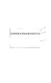
図1を参照すると、熱処理の適用下で変形するのに適切な構造体2が、基板1の面に形成されている。
Referring to FIG. 1, a
基板は、結晶構造(単結晶、多結晶、非晶質)が何であれ、任意の材料(半導体、金属など)であってよい。 The substrate may be any material (semiconductor, metal, etc.) whatever the crystal structure (single crystal, polycrystal, amorphous).
好ましくは、基板はSi、SiC又はGeなどの半導体材料、GaN、InGaN、GaAs又はInPなどのIV、II/VI又はIII/V型、及びこれらの元素の他の二元系、三元系又は四元系合金の基板で製造されている。 Preferably, the substrate is a semiconductor material such as Si, SiC or Ge, IV, II / VI or III / V type such as GaN, InGaN, GaAs or InP, and other binary, ternary or Manufactured with a quaternary alloy substrate.
特定の一実施形態によれば、基板から分離されるべきフィルムは複数の重層した半導体材料によって形成される、及び/又はオプトエレクトロニクス用途(例えば、LED又はレーザー用の)及び/又は光起電力用途(地上及び宇宙用途のための多重接合セルなどの)のための電子デバイスを備える、能動的フィルムである。フィルムはまた、特に電力用途の及び/又はマイクロシステムのための電子回路を備えてもよい。 According to one particular embodiment, the film to be separated from the substrate is formed by a plurality of stacked semiconductor materials and / or optoelectronic applications (eg for LEDs or lasers) and / or photovoltaic applications An active film with electronic devices (such as multi-junction cells for ground and space applications). The film may also comprise electronic circuitry, especially for power applications and / or for microsystems.
前記デバイスは、応力発生構造体が基板に結合される前に、引き離すフィルム中に、又は上に形成される。 The device is formed in or on the separating film before the stress generating structure is bonded to the substrate.
基板のへき開をもたらす応力を基板の面に伝達するように、基板の面にこの構造体を結合しなければならない。 This structure must be bonded to the surface of the substrate so that stresses that cause cleavage of the substrate are transmitted to the surface of the substrate.
したがって、構造体と基板との間で結合する適切な方法が選択される。 Accordingly, an appropriate method of coupling between the structure and the substrate is selected.
存在する材料に応じて、結合は分子接着(通常、ダイレクトボンディングと呼ばれる)、はんだ付け又は適切な接着剤、特に基板のへき開を引き起こすために行われる熱処理の温度に対して十分な耐性を有するものによって行うことができる。 Depending on the materials present, the bond is sufficiently resistant to the temperature of molecular bonding (usually called direct bonding), soldering or a suitable adhesive, especially the heat treatment performed to cause cleavage of the substrate Can be done by.
基板から引き離すフィルムから構造を除去しなければならない場合、可逆的に結合する接着剤、すなわち構造体を非破壊的に分解させられるものを用意することが好ましい。 If the structure must be removed from the film that is pulled away from the substrate, it is preferable to provide an adhesive that reversibly binds, i.e., one that can break down the structure non-destructively.
例えば、使用される接着剤はエポキシ系接着剤である。 For example, the adhesive used is an epoxy adhesive.
そのような接着剤は、加水分解することができるという利点を有する。したがって、これは、100℃で水蒸気の作用によって除去することができる。 Such an adhesive has the advantage that it can be hydrolyzed. It can therefore be removed by the action of water vapor at 100 ° C.
図1に示された実施形態において、構造体2は、結合層3によって基板1の面に結合されている。
In the embodiment shown in FIG. 1, the
しかし、結合層は問題の材料に応じて随意であり、ダイレクトボンディング作業は、基板の面に応力発生構造体を直接接触させることにより行われてもよい。 However, the bonding layer is optional depending on the material in question, and the direct bonding operation may be performed by bringing the stress generating structure directly into contact with the surface of the substrate.
構造体2は、例えば図3に示されるようなセル構造体であり、前記構造体を製造する方法は後で詳細に説明される。
The
セル2’の壁2’’は著しく異なる熱膨張係数を有する材料の二材料ストリップ(又は三材料ストリップでも)からなり、前記壁は基板の面に垂直である。 The wall 2 '' of the cell 2 'consists of a two-material strip (or even a three-material strip) of materials having significantly different coefficients of thermal expansion, said wall being perpendicular to the plane of the substrate.
「著しく異なる」という用語は、例えば、2種の材料の熱膨張係数間の比率が約2以上である、又は前記材料の熱膨張係数が反対符号であるということを意味すると理解される。 The term “significantly different” is understood to mean, for example, that the ratio between the thermal expansion coefficients of the two materials is about 2 or greater, or that the thermal expansion coefficients of the materials are of opposite sign.
応力発生構造体及び基板の間の界面は、セルの壁が基板に接している領域に限定されており、その結果、応力発生構造体は、基板に局部的に結合される。 The interface between the stress generating structure and the substrate is limited to the region where the cell walls are in contact with the substrate, so that the stress generating structure is locally coupled to the substrate.
基板のへき開をもたらすために、熱処理は、基板1の面と平行な平面の2方向に構造体2を変形させるのに適切な温度で適用される。
In order to bring about cleavage of the substrate, the heat treatment is applied at a temperature suitable for deforming the
非常に高い熱膨張係数を与えるセル構造体の形状によって、20〜500℃の間の温度は構造体を変形するのに一般に十分である。 Depending on the shape of the cell structure which gives a very high coefficient of thermal expansion, temperatures between 20 and 500 ° C. are generally sufficient to deform the structure.
温度はまた、基板に構造体を結合する任意の接着剤の性質に従って、接着剤が分解しないように選択される。 The temperature is also selected so that the adhesive does not decompose according to the nature of any adhesive that bonds the structure to the substrate.
したがって、接着剤がエポキシ系接着剤である場合、温度は、好ましくは300℃未満で適用される。 Therefore, when the adhesive is an epoxy adhesive, the temperature is preferably applied below 300 ° C.
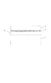
構造体2が基板1に結合されているので、この変形は基板の材料の機械的強さより大きい応力を基板中に生じさせ、結果として(基板の面に平行、ある深さで存在する)平面C内でへき開が引き起こされる。
Since the
基板が薄いほど、基板は可撓性があり基板中のへき開は深い。 The thinner the substrate, the more flexible the substrate and the deeper the cleavage in the substrate.
対照的に、より厚い基板はより浅いへき開を生じさせる。 In contrast, a thicker substrate causes a shallower cleavage.
図2から分かるように、へき開面Cは、次いで、続く使用のために引き離すことができるフィルム1’を画定し、ことによると機械的力を適用することにより、基板の残りからフィルムを分離する。
As can be seen from FIG. 2, the cleaved surface C then defines a
一旦フィルム1’が引き離されたなら、へき開のために役立った構造体2は除去することができる。
Once the film 1 'has been pulled away, the
構造体2が再使用されるようには意図されない場合、それは破壊的に、例えば材料の機械的な及び/又は化学的な除去によって除去することができる。
If the
しかし、また、再使用されることも構造体2にとって可能であり、その場合には、構造体2はフィルム1’から非破壊的に(例えば基板に構造体を結合するために使用される接着剤のエッチングによって)除去され、次いで、それを再使用する目的で調製される(例えば緩やかな研磨によって)。
However, it is also possible for the
構造体2が高価な場合、特に有利である。
It is particularly advantageous when the
別の可能性では、特に、引き離したフィルムの引き続きの使用の間に前記構造体が機能を果たした場合、構造体2は、引き離された1’から分離されない。
In another possibility, the
したがって、例えば、その透明構造体が光起電力フィルムの裏面に電気接触を作るのを可能にするという利点があれば、構造体2は保持され、光起電力フィルムのための支持体として役立つことができる。
Thus, for example, if the transparent structure has the advantage of allowing electrical contact to be made on the back side of the photovoltaic film, the
構造体2はまた、特にそれが自立する(すなわち、独立して扱うことができる)には厚さが薄過ぎる場合に、すなわち通常その厚さが50ミクロン未満である場合、引き離すフィルム1’を堅くするために役立つことができる。
The
適切な場合、さらなるフィルムをそこから引き離すために、基板の残りの部分が、新規の応力発生構造体に結合するために調製されてもよい。 Where appropriate, the remaining portion of the substrate may be prepared to bond to a new stress-generating structure in order to pull the additional film away from it.
それによりその方法は、インゴットが複数のフィルムに累進的に切断されることを可能にする。 The method thereby allows the ingot to be progressively cut into multiple films.
この方法の第1の利点は、使用される構造体が、その熱膨張係数を規定する際に選択の自由度を広げるということである。 The first advantage of this method is that the structure used gives more freedom of choice in defining its coefficient of thermal expansion.
特に、熱膨張係数を規定する基準は、使用される材料だけでなくまたセルの形状及び寸法である。 In particular, the criteria defining the coefficient of thermal expansion are not only the materials used, but also the shape and dimensions of the cells.
第2の利点は、使用される構造体が、それを構成する材料の個々の熱膨張係数よりはるかに高い熱膨張係数を有するということである。 A second advantage is that the structure used has a coefficient of thermal expansion that is much higher than the individual coefficient of thermal expansion of the material that comprises it.
さらに、構造体の材料及び形状を賢明に選択することによって、要件に応じて、正又は負の熱膨張係数を有する構造体を形成することができる。 Further, judicious selection of material and shape of the structure can form a structure having a positive or negative coefficient of thermal expansion, depending on requirements.
結果的に、先行技術においてよりも低い温度で加熱すれば、その機械的強さより高い応力を基板中に生じさせるのに十分である。 As a result, heating at a lower temperature than in the prior art is sufficient to cause a higher stress in the substrate than its mechanical strength.
したがって、基板がシリコンで製造されている場合、基板は室温で脆い。 Thus, if the substrate is made of silicon, the substrate is brittle at room temperature.
したがって、基板経由で応力を印加すると、仮に500℃を超える、すなわちシリコンの脆性展性遷移点を超える温度であった場合より、基板の容易なへき開をもたらす。 Therefore, when stress is applied via the substrate, the substrate is more easily cleaved than when the temperature exceeds 500 ° C., that is, exceeds the brittle malleability transition point of silicon.
さらに、より低い温度でのこの熱処理は、デバイスを損傷する又はそれらの性能に影響する危険性がないので、引き離すフィルム中又は上に形成される任意のデバイスにとって好都合である。
セル構造体
Furthermore, this heat treatment at lower temperatures is advantageous for any device formed in or on the film to be detached, as there is no risk of damaging the devices or affecting their performance.
Cell structure
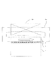
平面図の図3に示された一実施形態によれば、応力発生構造体は複数のセル2’を含むセル構造体であり、その壁2’’は、基板1の面に垂直な二材料ストリップ2a、2bである。
According to one embodiment shown in the plan view of FIG. 3, the stress generating structure is a cell structure comprising a plurality of
各二材料ストリップは、第1の熱膨張係数を有する第1の材料2a及び第1の熱膨張係数から著しく異なる第2の熱膨張係数を有する第2の材料2bから成る。
Each bi-material strip consists of a
有利なことに、セルは同一であり、基板の面と平行な平面内に画定されたパターンが繰り返されている。 Advantageously, the cells are identical and the pattern defined in a plane parallel to the plane of the substrate is repeated.
セル2’は、基板の面と平行な平面内で2方向に変形することができるのに適切な形状を有している。 The cell 2 'has an appropriate shape so that it can be deformed in two directions within a plane parallel to the surface of the substrate.
図3に示された例において、セルは連続的に凹凸の壁を有する、実質的に六角形の形状を有し、セルの内側にある材料は交互に材料2aと材料2bである。
In the example shown in FIG. 3, the cell has a substantially hexagonal shape with continuous irregular walls, and the material inside the cell is alternately material 2a and
しかしながら、八角形又は他の形状などのセルの他の形状を、本発明の範囲から離れることなく目論むことができる。 However, other shapes of cells such as octagons or other shapes can be envisioned without departing from the scope of the present invention.
科学文献において発表された数学的方法は、セルの形状及び寸法を規定する役目をする。 Mathematical methods published in the scientific literature serve to define the cell shape and dimensions.
そのような構造体を製作する方法は、図3に示されるA−A部の線上の図である、図4−1及び図4−2を参照して述べられる。 A method of manufacturing such a structure will be described with reference to FIGS. 4-1 and 4-2, which are diagrams on line AA shown in FIG.
図4−1(A)において示された第1のステップは、第1の材料2aの層から始まる。
The first step shown in FIG. 4-1 (A) starts with a layer of the
例えば、前記層は厚さが50μmのシリコン層である。 For example, the layer is a silicon layer having a thickness of 50 μm.
この層はトレンチT1、T2、T3を作り出すように深くエッチングされ、その通路は、これらのセルの壁を画定する。 This layer is deeply etched to create trenches T1, T2, T3, the passages defining the walls of these cells.
セルの形状及び寸法は、必要な熱膨張特性に従って前もって規定されている。 The cell shape and dimensions are predefined according to the required thermal expansion characteristics.
この目的のために、寸法は以下の刊行物に基づいてもよい:“Cellular solid structures with unbounded thermal expansion”by R.Lakes,Journal of Material Science Letters,15,475−477(1996);及び“Toward the topology design of mechanisms that exhibit snap−through behaviour” by T.E. Bruns and O.Sigmund,Computer Methods in Applied Mechanics and Engineering,Vol.193,Issues 36−38,10 September 2004,pp.3973−4000。 For this purpose, the dimensions may be based on the following publication: “Cellular solid structures with unbounded thermal expansion” by R.D. Lakes, Journal of Material Science Letters, 15, 475-477 (1996); and “Tow the theology design of mechanism exhibit struck-through-blow-through”. E. Bruns and O. Sigmad, Computer Methods in Applied Mechanics and Engineering, Vol. 193, Issues 36-38, 10 September 2004, pp. 3973-4000.
トレンチの幅は、例えば10μmである。 The width of the trench is, for example, 10 μm.
図4−1(B)において示された第2のステップにおいて、堆積された第2の材料2bは、その後いわゆる金属結合層(例えば、およそ10mmのチタン)と呼ばれ、トレンチの壁に真空蒸着又はスパッタによって堆積されている。
In the second step shown in FIG. 4-1 (B), the deposited
例えば、第2の材料は、シリコンの熱膨張係数より大きい熱膨張係数を有する金属(アルミニウム又は銀などの)である。 For example, the second material is a metal (such as aluminum or silver) having a coefficient of thermal expansion greater than that of silicon.
この堆積作業は、第2の材料2bのトレンチT1、T2、T3を充填する効果、及びまた第2の材料2bの層で第1の材料2aの面を被覆する効果がある。
This deposition operation has the effect of filling the trenches T1, T2, T3 of the
図4−2(C)に示された第3のステップにおいて、第1の材料2aの面を被覆している過剰の第2の材料は、CMP(化学的な機械研磨)によって除去される。
In the third step shown in FIG. 4-2 (C), the excess second material covering the surface of the
この段階で、そのように堆積させた金属の密度を高めるために、不活性雰囲気中で低温(すなわちアルミニウムの場合、通常およそ200℃で)で、場合によって、熱アニール作業が行われる。 At this stage, in order to increase the density of the metal so deposited, a thermal annealing operation is optionally performed at a low temperature (ie, typically about 200 ° C. for aluminum) in an inert atmosphere.
次に、図4−2(D)を参照して、レジストマスク4を第1の材料2aの層に堆積する。
Next, referring to FIG. 4D, a resist mask 4 is deposited on the layer of the
このマスクは最終のセル構造体2に保持することが所望される第1の材料2aの部分を覆うように選択的に堆積する。
This mask is selectively deposited so as to cover the portion of the
前記部分は、二材料ストリップを第2の材料2bとともに構成するように、第2の材料2bで充填されたトレンチに隣接している。
Said part is adjacent to a trench filled with the
通常、前記部分の幅は約10μmである。 Usually, the width of the part is about 10 μm.
レジストマスクは、続くエッチングステップの間に、第2の材料2bに隣接している第1の材料2aを保護するように意図される。
The resist mask is intended to protect the
図4−2(E)を参照すると、マスク4によって保護されていない第1の材料2aは、前記第2の材料2bに関して選択的にエッチングされる。
Referring to FIG. 4E, the
最終ステップ(ここに図示されず)において、マスク4は除去される。 In the final step (not shown here), the mask 4 is removed.
したがって、複数のセル2’、壁2”(二材料ストリップ2a、2bである)から成るセル構造体が得られる。
Thus, a cell structure consisting of a plurality of cells 2 ',
次いで、前記構造体は任意の適切なボンディング法によって基板1の面に結合される。
The structure is then bonded to the surface of the
述べた場合において、構造体は基板から独立して製作され、次いで、基板に結合される。 In the case described, the structure is fabricated independently from the substrate and then bonded to the substrate.
しかし、第1の材料2aの層を基板の面に結合又は堆積し、セル構造体を製作するために上述と同様の方法をこの層に適用することも可能である。
However, it is also possible to bond or deposit a layer of the
このようにして、第1の材料2aの層を、スパッタによって、好ましくはCVD(化学蒸着)によって、又は電気化学的方法によって基板1の面に堆積し、次に、セル構造体を形成させるエッチング作業を行ってもよい。
In this way, a layer of the
セル構造体を結合する前に又はセル構造体が形成される第1の材料2aを堆積させるために、応力発生構造体への結合を促進する及び/又は応力発生構造体を構成する材料によって、何らかの汚染からそれを保護するために基板の面を調製することは有利である。
Before bonding the cell structure or for depositing the
例えば、およそ500ナノメートルの厚さを有する酸化シリコンの保護層が形成されてもよい。これはCVD技法によって堆積される、又は基板がシリコンで製造されている場合には、熱的酸化によって形成される。 For example, a protective layer of silicon oxide having a thickness of approximately 500 nanometers may be formed. This is deposited by CVD techniques or by thermal oxidation if the substrate is made of silicon.
また、前記側面層に100〜300オングストロームの厚さでフラッシュ蒸発ステップによってチタン結合層を形成し、応力発生構造体の金属への結合を促進することが可能である。 In addition, a titanium bonding layer may be formed on the side layer by a flash evaporation step with a thickness of 100 to 300 angstroms to promote bonding of the stress generating structure to the metal.
さらに、デバイスは、引き離すフィルム中に又は上に形成され、基板の面は、もはや平面でなく応力発生構造体に結合するには適切でない。 Furthermore, the device is formed in or on the film to be pulled away, and the surface of the substrate is no longer flat and is not suitable for bonding to the stress generating structure.
したがって、SiO2の層はデバイスの高さを超えて面に堆積され、次いで前記層は、応力発生構造体に結合する目的で、例えば研磨によって平坦化される。 Thus, a layer of SiO 2 is deposited on the surface beyond the height of the device, and the layer is then planarized, eg by polishing, for the purpose of bonding to the stress generating structure.
へき開作業の後、エッチングにより酸化物層を除去することは可能で、それによって、応力発生構造体を除去することがより容易になる。 After the cleaving operation, it is possible to remove the oxide layer by etching, which makes it easier to remove the stress generating structure.
図3は、得られた直線/セル状構造集合体の平面図(すなわち基板1の面に垂直な方向に沿った)を示す。 FIG. 3 shows a plan view of the resulting linear / cellular structure assembly (ie, along a direction perpendicular to the surface of the substrate 1).
熱処理を適用すると、二材料ストリップの第2の材料2bは、その熱膨張係数がより高いので、第1の材料より伸び、それによって、引張力を生じ、各セル2’の壁が実質的に直線になるまで伸びる。
When heat treatment is applied, the
セルの壁が基板の面に結合されているので、伸びは基板内の応力の印加を引き起こし、へき開をもたらす。 Since the cell walls are bonded to the surface of the substrate, the elongation causes the application of stress in the substrate, resulting in cleavage.
したがって、各二材料ストリップによって応力は、基板に、一様にではなく局部的に伝達される。 Thus, each bi-material strip transmits stress to the substrate locally rather than uniformly.
言いかえれば、各二材料ストリップ2a及び2bは、それが結合されている基板に離散的な応力を働かせ、そのように働く離散的な応力はすべて組み合わされ、へき開面Cにおいて、基板の材料の機械的強さより高い全体応力を生じさせる。
使用した材料の組の例
In other words, each
Example of material set used
二材料ストリップを構成する材料には、可能な限り異なる膨張係数を有さなければならない。 The materials making up the bi-material strip must have as different expansion coefficients as possible.
2種の材料の熱膨張係数間で約2以上の比率が望ましい。 A ratio of about 2 or greater between the thermal expansion coefficients of the two materials is desirable.
したがって、二材料ストリップの材料の一方がシリコン(25℃でTECは約4.6×10⁻⁶K−1である)である場合、他方の材料は、有利には、銀(TECおよそ18×10−6K−1)、アルミニウム(TECおよそ23×10−6K−1)から、又は銅(TECおよそ16.5×10⁻⁶K−1)からでも、選択される。 Thus, if one of the materials of the bi-material strip is silicon (the TEC is about 4.6 × 10 −6 K −1 at 25 ° C.), the other material is advantageously silver (TEC approximately 18 × 10 −6 K −1 ), aluminum (TEC approximately 23 × 10 −6 K −1 ), or copper (TEC approximately 16.5 × 10 −6 K −1 ).
これらの場合において、シリコンは他方の材料ほどは膨張しない構造体が得られる。 In these cases, silicon is obtained that does not expand as much as the other material.
また、逆の方向に振る舞う構造体を考案して、二材料ストリップを形成するために、シリコン及びシリコンより実質的に低い熱膨張係数を有する材料を使用することも可能である。 It is also possible to devise structures that behave in the opposite direction and use silicon and materials having a coefficient of thermal expansion substantially lower than silicon to form a bi-material strip.
これは、特に酸化シリコン(SiO2)及び窒化ケイ素(SixNy)の場合である。 This is especially the case for silicon oxide (SiO 2 ) and silicon nitride (Si x N y ).
また、ゲルマニウム(TECおよそ6.1×10⁻⁶K−1)を二材料ストリップの材料の一方に、及び他方の材料のために上述の金属の1つを、又は、鉄(TECおよそ11.8×10⁻⁶K−1)さえ使用することが可能である。 Also, germanium (TEC approximately 6.1 × 10 −6 K −1 ) in one of the materials of the bi-material strip and one of the metals described above for the other material, or iron (TEC approximately 11. Even 8 × 10 −6 K −1 ) can be used.
一変形として、サファイアが二材料ストリップの材料の一方のために、上述の金属の1つが他方の材料のために選択されてもよい。 As a variant, sapphire may be selected for one of the materials of the bi-material strip and one of the above mentioned metals for the other material.
最終的に、二材料ストリップの一方の材料のために、負の熱膨張係数を有する材料(タングステン酸ジルコニウムZrW2O8などの)を、正の熱膨張係数を有する材料(例えば銀)と組み合わせて使用することが可能である。 Finally, for one material of the bi-material strip, combine a material with a negative coefficient of thermal expansion (such as zirconium tungstate ZrW 2 O 8 ) with a material with a positive coefficient of thermal expansion (eg silver) Can be used.
そのような二材料ストリップの利点は、大きい変形を得るためにそれを強く加熱することが必要ではなく、それによって、シリコンが脆くなる500℃未満の温度範囲でシリコンをへき開するのに特に適切にすることである。 The advantage of such a bi-material strip is that it is not particularly necessary to cleave the silicon in a temperature range below 500 ° C. where it does not need to be heated strongly to obtain a large deformation, thereby making the silicon brittle. It is to be.
また、壁が三材料ストリップであるセル構造体を製作することも可能であり、そこでは、二材料ストリップを形成する第1、及び第2の材料は、それぞれ高い正の熱膨張係数を有する材料(銀などの)及び負の熱膨張係数を有する材料であり、これらはシリコンなどの第3の材料によって隔てられている。 It is also possible to fabricate a cell structure whose walls are three material strips, where the first and second materials forming the two material strips are each a material having a high positive coefficient of thermal expansion. A material having a negative thermal expansion coefficient (such as silver) and separated by a third material such as silicon.
中位の熱膨張係数を有するシリコンでは、安定性と機械的強さとを有するそのような構造体を適用する。 For silicon with a moderate coefficient of thermal expansion, such a structure with stability and mechanical strength is applied.
代替として、セル構造体は、二材料ストリップを形成する第1及び第2の材料が空洞によって隔てられている、三材料ストリップ壁で形成されてもよい。 Alternatively, the cell structure may be formed of a three material strip wall in which the first and second materials forming the two material strip are separated by a cavity.
そのような構造体は、O.Sigmund and S.Torquato“Composites with extremal thermal expansion coefficients”,Appl.Phys.Lett.69(21),18 Nov.1996及び“Design of materials with extreme thermal expansion using a three−phase topology optimization method”,J.Mech.Phys.Solids,Vol.45,No.6,pp.1037−1067,1997.による刊行物に記載されている。
磁気歪みセル構造体
Such structures are O.D. Sigmand and S.M. Torquato "Composites with extreme thermal expansion coefficients", Appl. Phys. Lett. 69 (21), 18 Nov. 1996 and “Design of materials with extreme expansion using a three-phase topology optimization method”, J. Am. Mech. Phys. Solids, Vol. 45, no. 6, pp. 1037-1067, 1997. It is described in the publication by.
Magnetostrictive cell structure
本発明の特に有利な一実施形態によれば、応力発生構造体はまた、磁界の作用下で変形するように設計されている。 According to a particularly advantageous embodiment of the invention, the stress generating structure is also designed to deform under the action of a magnetic field.
この目的のために、二材料ストリップを構成する材料の一方は、磁気歪み材料であり、二材料ストリップの他方の構成材料の熱膨張係数とは著しく異なる熱膨張係数をなお有している。 For this purpose, one of the materials constituting the bi-material strip is a magnetostrictive material and still has a coefficient of thermal expansion that is significantly different from that of the other material of the bi-material strip.
好ましくは、磁気歪み材料は、絶対値で0.02%より大きい伸びを有する材料、好ましくは「巨大な」磁気歪みと呼ばれるものを示す、すなわち絶対値で50ppmより大きい磁気歪み係数を有する材料から選択される。 Preferably, the magnetostrictive material is from a material having an elongation of greater than 0.02% in absolute value, preferably what is referred to as “giant” magnetostriction, ie having a magnetostriction coefficient of greater than 50 ppm in absolute value. Selected.
希土類/鉄合金系材料はそのような特性を示すと知られている。 Rare earth / iron alloy materials are known to exhibit such properties.
本発明を実施するのに非常に適切な磁気歪み材料の一例は、ターフェノールDであり、これは、式Tb0,3Dy0,7Fe19を有する希土類/鉄合金であり、多結晶形態又は非晶質形態で使用することができる。 One example of a magnetostrictive material that is very suitable for practicing the present invention is terphenol D, which is a rare earth / iron alloy having the formula Tb 0,3 Dy 0,7 Fe 19 , a polycrystalline form Or it can be used in an amorphous form.
磁気歪み係数は各形態(結晶及び非晶質の)に対して異なるが、いずれも50ppmより大きい。 The magnetostriction coefficient is different for each form (crystalline and amorphous), but both are greater than 50 ppm.
その結晶性形態において、磁界の作用下で伸びは最大0.2%であり、およそ1kN/cmの圧縮応力場を生じさせる。 In its crystalline form, the elongation is up to 0.2% under the action of a magnetic field, producing a compressive stress field of approximately 1 kN / cm.
負の伸びを有するSmFe2、及び正の伸びを有するDyFe2及びTbFe2などの他の希土類/鉄合金はまた、本発明を実施するのに非常に適切である。 Other rare earth / iron alloys such as SmFe 2 with negative elongation and DyFe 2 and TbFe 2 with positive elongation are also very suitable for practicing the present invention.
そのとき二材料ストリップの他方の材料は、通常、シリコン、SiC又はゲルマニウムである。 The other material of the bimaterial strip is then usually silicon, SiC or germanium.
セル構造体は上述のそれと同一の方法によって製作されてもよい。 The cell structure may be fabricated by the same method as described above.
例を挙げると、シリコンストリップの厚さが50ミクロンでありターフェノールDストリップの厚さが15ミクロンである、シリコン/ターフェノールD二材料ストリップから成る壁を有する構造体を形成することができる。 By way of example, a structure can be formed having a wall of silicon / terphenol D bimaterial strips with a silicon strip thickness of 50 microns and a terphenol D strip thickness of 15 microns.
このようにして形成された構造体は、温度(そのとき、それを変形するために熱処理のみが使用される場合よりも低くてもよい)、及び磁界を組み合わたせ作用下で変形することができる。 The structure thus formed can be deformed under the action of a combination of temperature (which may then be lower than if only heat treatment is used to deform it) and a magnetic field. .
そのようなセル構造体の全体の変形は、磁界の作用下で磁気歪み材料の固有の変形より大きい。 The overall deformation of such a cell structure is greater than the inherent deformation of the magnetostrictive material under the action of a magnetic field.
例えば、構造体の寸法の相対的な増加は、磁気歪み材料の相対的伸びより10〜100倍大きくすることができる。 For example, the relative increase in structure dimensions can be 10 to 100 times greater than the relative elongation of the magnetostrictive material.
この増幅率は、セルの幾何学的設計及びこれらの格子配置に依存する。 This amplification factor depends on the cell's geometric design and their lattice arrangement.
この増幅は、構造体が温度の作用のみにより膨張又は収縮をする先の実施形態と比較して、応力を発生する構造体の所与の膨脹又は収縮のために、基板中又は基板上の温度に非常に敏感な電子デバイスの存在と両立する、より低い温度の熱処理の適用を可能にする。 This amplification is due to the temperature in or on the substrate for a given expansion or contraction of the structure generating the stress compared to the previous embodiment where the structure expands or contracts only by the effect of temperature. Enables the application of lower temperature heat treatments that are compatible with the presence of highly sensitive electronic devices.
そのような構造体を有する基板をへき開するために、熱処理及び磁界が同時に適用される。 In order to cleave the substrate having such a structure, a heat treatment and a magnetic field are applied simultaneously.
適用される温度は、応力を発生する構造体の磁気特性を損なわないように、磁気歪み材料のキュリー温度Tcよりかなり低くなければならない。 The applied temperature must be significantly lower than the Curie temperature Tc of the magnetostrictive material so as not to impair the magnetic properties of the stress-generating structure.
ターフェノールDの場合には、キュリー温度は380℃であり、その結果、熱処理は350℃を超える温度では適用されず、好ましくは300℃未満の温度で適用される。 In the case of terphenol D, the Curie temperature is 380 ° C., so that heat treatment is not applied at temperatures above 350 ° C., preferably at temperatures below 300 ° C.
DyFe2、SmFe2及びTbFe2については、キュリー温度が630〜710℃の間にあり、したがって、熱処理は好ましくは600℃未満の温度で適用される。 For DyFe 2 , SmFe 2 and TbFe 2 , the Curie temperature is between 630 and 710 ° C., so the heat treatment is preferably applied at a temperature below 600 ° C.
図5を参照すると、磁界は、応力を発生する構造体2を取り巻き伝導コイル5bに取り囲まれている磁気回路5aによって印加される。
Referring to FIG. 5, the magnetic field is applied by a
水平の矢印によって示されるように、このデバイスは基板の面と平行な磁気誘導を生じさせる。 As indicated by the horizontal arrow, this device produces a magnetic induction parallel to the plane of the substrate.
基板が細長い形状を有する、すなわち面(そのとき基板は、ことによると一次元であると考えられる)に平行な平面内の2つの垂線方向に沿った基板の寸法の比率が、少なくとも10である場合、印加磁界は静的であることが好ましく、基板の最長寸法に平行に向けられる。 The substrate has an elongated shape, i.e. the ratio of the dimensions of the substrate along two perpendicular directions in a plane parallel to the plane (the substrate is possibly considered one-dimensional) is at least 10. In some cases, the applied magnetic field is preferably static and is oriented parallel to the longest dimension of the substrate.
面に平行な平面内の2つの垂線方向に沿った基板の寸法が、同じ程度の大きさである場合(例えば、基板が円板の形態をとる場合)、磁界は、基板の平面内において回転する磁気誘導を作り出す変動場の組み合わせの形態で印加され、応力発生構造体の2方向に沿って膨脹を引き起こす。 If the dimensions of the substrate along two perpendicular directions in a plane parallel to the plane are of the same magnitude (eg if the substrate takes the form of a disk), the magnetic field rotates in the plane of the substrate. Applied in the form of a combination of fluctuating fields that create magnetic induction that causes expansion along two directions of the stress generating structure.
必要な磁気誘導は通常0.1〜1テスラである。 The required magnetic induction is usually 0.1 to 1 Tesla.
磁気処理の1つの利点は、応力発生構造体又はへき開される基板とのいずれの接触も伴わないで、それを行うことができるということであり、それによって、その実施を容易にする。
基板の予備脆化
One advantage of magnetic processing is that it can be done without any contact with the stress generating structure or the substrate to be cleaved, thereby facilitating its implementation.
Pre-embrittlement of substrate
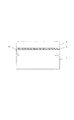
本発明の特定の一実施形態によれば、基板は、そのへき開を容易にする目的で熱処理(及び適切な場合には磁界)を適用する前に脆化されてもよい。 According to one particular embodiment of the invention, the substrate may be embrittled prior to applying a heat treatment (and magnetic field where appropriate) to facilitate its cleavage.
図6に示されるように、弱いゾーン10は、へき開面に対応する平面内の基板中に形成される。
As shown in FIG. 6, the
脆化は、場合によって熱処理と組み合わせたイオン注入に由来してもよく、へき開面に対応する平面中に、恐らく、細孔及び/又は微小バブルが結果として生成する。 Embrittlement may result from ion implantation, optionally in combination with heat treatment, possibly resulting in pores and / or microbubbles in the plane corresponding to the cleavage plane.
この場合、注入されるイオン線量は、スマートカット(商標)技術において破砕のために必要とされるそれより約10倍小さい。 In this case, the implanted ion dose is about 10 times smaller than that required for disruption in the Smart Cut ™ technology.
例えば、シリコン中で20ミクロンの深さでスマートカット(商標)破砕するためのH+イオン注入線量は、およそ1017原子/cm2であるが、本発明に従って予備脆化するのに必要とされる線量はおよそ5×1015〜1016原子/cm2である。 For example, the H + ion implantation dose for SmartCut ™ fracture in silicon at a depth of 20 microns is approximately 10 17 atoms / cm 2 , but is required to pre-brittle according to the present invention. The dose is about 5 × 10 15 to 10 16 atoms / cm 2 .
前記脆化処理はまた、基板の製造中に行われてもよい。 The embrittlement process may also be performed during the manufacture of the substrate.
したがって、例えば、脆化ゾーンは、シリコン基板上に、SixGe1−x(式中、0<x<0.8)の2μm厚さのエピタキシー成長させた層によって形成されてもよい。この層は、層の中央では最大のゲルマニウム含有率(最大20%)を有し、上側及び下側の界面に接近するにつれて約5%まで低下する。 Thus, for example, the embrittlement zone may be formed by a 2 μm thick epitaxially grown layer of Si x Ge 1-x (where 0 <x <0.8) on a silicon substrate. This layer has the highest germanium content (up to 20%) in the middle of the layer and drops to about 5% as the upper and lower interfaces are approached.
例えば、厚さ20μmの別のシリコン層が前記層にエピタキシー成長される。 For example, another silicon layer with a thickness of 20 μm is epitaxially grown on said layer.
SixGe1−x層中のゲルマニウム勾配は、続いて引き離されるように意図される下側にあるSi層の十分な結晶品質(すなわちより低い転位密度及び亀裂の欠如)でエピタキシャル成長するように選択される。 The germanium gradient in the Si x Ge 1-x layer is selected to grow epitaxially with sufficient crystal quality (ie lower dislocation density and lack of cracks) of the underlying Si layer intended to be subsequently detached. Is done.
SixGe1−x格子パラメータのこの濃度勾配は、転位の形成によって層に応力緩和を作り出すことなく、下側にあるシリコンの格子定数に連続的に一致させることが、実際可能である。 It is practically possible for this concentration gradient of the Si x Ge 1-x lattice parameter to continuously match the underlying silicon lattice constant without creating stress relaxation in the layer due to the formation of dislocations.
SixGe1−x層は、上側及び下側にあるシリコンの層より機械的に脆く、へき開は前記SixGe1−x層内で起こる。
基板中の破砕イニシエータ
The Si x Ge 1-x layer is mechanically more fragile than the upper and lower silicon layers, and cleavage occurs within the Si x Ge 1-x layer.
Crushing initiator in substrate
代替として、へき開作業は、所望の深さで基板中に破砕イニシエータを用意することにより容易にすることができる。 Alternatively, the cleaving operation can be facilitated by providing a crushing initiator in the substrate at the desired depth.
図7に示されるように、破砕イニシエータは、応力を発生する構造体が破砕(上述の平面C)を引き起こさなければならない深さに実質的に対応する深さで、基板1の側面に付けられた切欠き11(通常、深さ数十ミクロンの)の形態をとってもよい。
As shown in FIG. 7, the crushing initiator is applied to the side of the
応力が非常に高い深さの範囲内では、基板中の破砕の位置のために、そのようなイニシエータは正確な位置決めを可能にする。 Within a very high stress depth, such initiators allow for precise positioning due to the location of the fracture in the substrate.
また、それは、へき開のために印加される応力場を、したがって温度、適切な場合には磁気誘導を低減することを可能にする。 It also makes it possible to reduce the stress field applied for cleavage, and thus the temperature, and where appropriate magnetic induction.
破砕イニシエータは、機械的手段によって切削する手法を使用して、及び/又は化学的手段によって、生成することができる。 The crushing initiator can be generated using techniques that cut by mechanical means and / or by chemical means.
例えば、所望の破砕深さに対応する、約2ミクロンの厚さのp+ドープシリコンの層を含むn型シリコンのウェーハには、切欠きを形成するためにピロカテコールを使用する選択エッチングが、p+ドープシリコン層の周辺で行われる。 For example, an n-type silicon wafer containing a layer of p + doped silicon about 2 microns thick, corresponding to the desired crushing depth, can be selectively etched using pyrocatechol to form a notch. Performed around the p + doped silicon layer.
この切欠きの深さは、化学エッチングの継続時間に依存する。 The depth of this notch depends on the duration of chemical etching.
通常、浴内で撹拌しながら10分間エッチングする場合、およそ50ミクロンの深さを有する切欠きを形成することができる。 Typically, when etching for 10 minutes with stirring in a bath, a notch having a depth of approximately 50 microns can be formed.
シリコン基板をへき開するために、図3に平面図で示すようなセル構造体を形成する。 In order to cleave the silicon substrate, a cell structure as shown in a plan view in FIG. 3 is formed.
セルの壁をシリコン2a/銀2b二材料ストリップから形成する。
The cell walls are formed from a
シリコン及び銀のストリップの幅は約10ミクロンである。 The width of the silicon and silver strip is about 10 microns.
セル構造体の厚さ(基板の面に垂直な方向の)は、約40ミクロンである。 The thickness of the cell structure (in the direction perpendicular to the plane of the substrate) is about 40 microns.
各セルを直径100ミクロンの円に刻み、セルの各側面は長さ約50ミクロンを有し、約10ミクロンのたるみのある曲線を描く。 Each cell is cut into a 100 micron diameter circle, each side of the cell has a length of about 50 microns and draws a sag curve of about 10 microns.
二材料ストリップからの銀による基板の潜在的な汚染を回避するために、基板に構造体を結合する前に、シリコン基板の面に保護酸化物層を形成するのが好ましく、前記酸化物層は、基板をへき開し引き離すフィルムから構造体を除去した後に、ことによると除去される。 In order to avoid potential contamination of the substrate by silver from the bi-material strip, it is preferred to form a protective oxide layer on the surface of the silicon substrate before bonding the structure to the substrate, the oxide layer being After removing the structure from the film that cleaves and separates the substrate, it is possibly removed.
このセル構造体は、正に室温から高い接着エネルギー密度を与えることができるダイレクトボンディング法、例えば、プラズマ処理によって調製した面を用いる接着法によって、基板の面に結合する。この種の処理によって数百mJ/m2の接着エネルギー密度を得ることができることは公知である。 This cell structure is bonded to the surface of the substrate by a direct bonding method that can give a high bonding energy density from just room temperature, for example, a bonding method using a surface prepared by plasma treatment. It is known that an adhesion energy density of several hundred mJ / m 2 can be obtained by this type of treatment.
そのとき、接着工程(すなわち接着エネルギーの増加)は、セル構造体の変形の何らかの寄生効果が、結合界面で実質的に働き得る前に接着工程を完全に終了させるために、十分に時間をかけた温度での温度上昇率(通常5℃/分)を使用して、集合体の温度を上げることにより行う。 At that time, the bonding process (ie increasing the bonding energy) takes sufficient time to completely complete the bonding process before any parasitic effects of deformation of the cell structure can substantially work at the bonding interface. This is done by raising the temperature of the assembly using the rate of temperature rise at normal temperature (usually 5 ° C./min).
次いで、集合体を約450℃の温度に加熱する。 The assembly is then heated to a temperature of about 450 ° C.
この温度は、二材料ストリップの銀に対して十分に緩やかであり、前述の保護層を通して基板を汚染することはない。 This temperature is sufficiently gentle for the bi-material strip of silver and does not contaminate the substrate through the protective layer described above.
この加熱の作用下で銀のストリップは、シリコンストリップより伸び、それによって、これらが実質的に直線になるまで、湾曲した壁を伸ばす。 Under the action of this heating, the silver strip extends beyond the silicon strip, thereby stretching the curved walls until they are substantially straight.
この変形によってシリコン基板中に応力を生じ、50〜100ミクロンの深さでへき開することが可能になる。 This deformation creates a stress in the silicon substrate that can be cleaved at a depth of 50-100 microns.
1・・・基板、1’・・・フィルム、2・・・応力発生構造体、3・・・結合層、C・・・へき開面。
DESCRIPTION OF
Claims (30)
(i)局部的に基板(1)の面に結合され、熱処理の作用下で基板(1)の面と平行な平面内で膨脹又は収縮するように設計された応力発生構造体(2)と呼ばれるものを形成するステップと、
(ii)膨張又は収縮を引き起こすように設計された前記構造体(2)に熱処理を適用し、基板(1)中に複数の局部応力を生じさせ、応力の組合せが引き離すフィルム(1’)を画定する基板の面と平行なへき開面(C)での基板の機械的強さより大きい応力を生じさせ、前記応力が前記平面(C)にわたって基板(1)のへき開をもたらすステップと、
を含む方法。 A method for cleaving the substrate (1) to separate the film (1 ′) from the substrate (1), comprising the following sequential steps:
(I) a stress generating structure (2) coupled locally to the surface of the substrate (1) and designed to expand or contract in a plane parallel to the surface of the substrate (1) under the action of heat treatment; Forming what is called,
(Ii) applying a heat treatment to the structure (2) designed to cause expansion or contraction, producing a plurality of local stresses in the substrate (1), and the film (1 ′) from which the combination of stresses separates Producing a stress greater than the mechanical strength of the substrate at a cleavage plane (C) parallel to the surface of the defining substrate, said stress causing cleavage of the substrate (1) across said plane (C);
Including methods.
Applications Claiming Priority (2)
| Application Number | Priority Date | Filing Date | Title |
|---|---|---|---|
| FR1061052 | 2010-12-22 | ||
| FR1061052A FR2969664B1 (en) | 2010-12-22 | 2010-12-22 | METHOD FOR CLEAVING A SUBSTRATE |
Publications (2)
| Publication Number | Publication Date |
|---|---|
| JP2012134459A true JP2012134459A (en) | 2012-07-12 |
| JP5458362B2 JP5458362B2 (en) | 2014-04-02 |
Family
ID=43927597
Family Applications (1)
| Application Number | Title | Priority Date | Filing Date |
|---|---|---|---|
| JP2011241537A Active JP5458362B2 (en) | 2010-12-22 | 2011-11-02 | Method for cleaving a substrate |
Country Status (8)
| Country | Link |
|---|---|
| US (1) | US8420506B2 (en) |
| EP (1) | EP2468931B1 (en) |
| JP (1) | JP5458362B2 (en) |
| KR (1) | KR101401580B1 (en) |
| CN (1) | CN102543678B (en) |
| FR (1) | FR2969664B1 (en) |
| SG (1) | SG182051A1 (en) |
| TW (1) | TW201230181A (en) |
Cited By (2)
| Publication number | Priority date | Publication date | Assignee | Title |
|---|---|---|---|---|
| KR101372395B1 (en) * | 2013-01-09 | 2014-03-10 | 한국과학기술원 | Method for separating nanogenerator and method for manufacturing nanogenerator using the same |
| KR101547057B1 (en) | 2014-02-12 | 2015-08-24 | 한국과학기술원 | Method for separating nanogenerator and method for manufacturing nanogenerator using the same |
Families Citing this family (11)
| Publication number | Priority date | Publication date | Assignee | Title |
|---|---|---|---|---|
| US20120217622A1 (en) * | 2010-05-21 | 2012-08-30 | International Business Machines Corporation | Method for Imparting a Controlled Amount of Stress in Semiconductor Devices for Fabricating Thin Flexible Circuits |
| FR2978600B1 (en) | 2011-07-25 | 2014-02-07 | Soitec Silicon On Insulator | METHOD AND DEVICE FOR MANUFACTURING LAYER OF SEMICONDUCTOR MATERIAL |
| US8709957B2 (en) * | 2012-05-25 | 2014-04-29 | International Business Machines Corporation | Spalling utilizing stressor layer portions |
| FR3007892B1 (en) * | 2013-06-27 | 2015-07-31 | Commissariat Energie Atomique | METHOD FOR TRANSFERRING A THIN LAYER WITH THERMAL ENERGY SUPPLY TO A FRAGILIZED AREA VIA AN INDUCTIVE LAYER |
| CN105981132B (en) * | 2014-02-18 | 2019-03-15 | 日本碍子株式会社 | The operation substrate and semiconductor composite substrate of semiconductor composite substrate |
| JP6396852B2 (en) * | 2015-06-02 | 2018-09-26 | 信越化学工業株式会社 | Method for manufacturing composite wafer having oxide single crystal thin film |
| CN107230611A (en) * | 2016-03-25 | 2017-10-03 | 松下知识产权经营株式会社 | Group III-nitride process for producing crystal and RAMO4Substrate |
| CN107785244A (en) * | 2017-09-27 | 2018-03-09 | 厦门三安光电有限公司 | A kind of semiconductor epitaxial growth method and its graphite carrier |
| JP7373267B2 (en) * | 2018-03-29 | 2023-11-02 | リンテック株式会社 | Manufacturing method of individual pieces |
| CN109554668A (en) * | 2018-12-17 | 2019-04-02 | 合肥鑫晟光电科技有限公司 | The method of crucible nozzle arrangements, crucible and nozzle clearing |
| CN114639635B (en) * | 2022-03-17 | 2023-03-21 | 电子科技大学 | Method for peeling single crystal thin film, single crystal thin film and electronic component |
Citations (1)
| Publication number | Priority date | Publication date | Assignee | Title |
|---|---|---|---|---|
| US20070249140A1 (en) * | 2006-04-19 | 2007-10-25 | Interuniversitair Microelecktronica Centrum (Imec) | Method for the production of thin substrates |
Family Cites Families (11)
| Publication number | Priority date | Publication date | Assignee | Title |
|---|---|---|---|---|
| FR2681472B1 (en) | 1991-09-18 | 1993-10-29 | Commissariat Energie Atomique | PROCESS FOR PRODUCING THIN FILMS OF SEMICONDUCTOR MATERIAL. |
| SG67458A1 (en) * | 1996-12-18 | 1999-09-21 | Canon Kk | Process for producing semiconductor article |
| KR100529742B1 (en) | 2000-08-01 | 2005-11-17 | 존 울프 인터내셔날 인코포레이티드 | Manufacturing method of a thin film on a substrate |
| US7176528B2 (en) * | 2003-02-18 | 2007-02-13 | Corning Incorporated | Glass-based SOI structures |
| JP2006024782A (en) | 2004-07-08 | 2006-01-26 | Sharp Corp | Substrate manufacturing method and apparatus |
| TW200703462A (en) * | 2005-04-13 | 2007-01-16 | Univ California | Wafer separation technique for the fabrication of free-standing (Al, In, Ga)N wafers |
| JP5064692B2 (en) * | 2006-02-09 | 2012-10-31 | 信越化学工業株式会社 | Manufacturing method of SOI substrate |
| US9362439B2 (en) | 2008-05-07 | 2016-06-07 | Silicon Genesis Corporation | Layer transfer of films utilizing controlled shear region |
| US8703521B2 (en) | 2009-06-09 | 2014-04-22 | International Business Machines Corporation | Multijunction photovoltaic cell fabrication |
| US20110048517A1 (en) | 2009-06-09 | 2011-03-03 | International Business Machines Corporation | Multijunction Photovoltaic Cell Fabrication |
| US20100310775A1 (en) | 2009-06-09 | 2010-12-09 | International Business Machines Corporation | Spalling for a Semiconductor Substrate |
-
2010
- 2010-12-22 FR FR1061052A patent/FR2969664B1/en not_active Expired - Fee Related
-
2011
- 2011-11-02 JP JP2011241537A patent/JP5458362B2/en active Active
- 2011-11-18 SG SG2011085628A patent/SG182051A1/en unknown
- 2011-11-23 TW TW100142965A patent/TW201230181A/en unknown
- 2011-11-29 US US13/306,591 patent/US8420506B2/en active Active
- 2011-12-05 KR KR1020110129054A patent/KR101401580B1/en active IP Right Grant
- 2011-12-21 CN CN201110433265.7A patent/CN102543678B/en active Active
- 2011-12-22 EP EP11195129.9A patent/EP2468931B1/en active Active
Patent Citations (1)
| Publication number | Priority date | Publication date | Assignee | Title |
|---|---|---|---|---|
| US20070249140A1 (en) * | 2006-04-19 | 2007-10-25 | Interuniversitair Microelecktronica Centrum (Imec) | Method for the production of thin substrates |
Cited By (2)
| Publication number | Priority date | Publication date | Assignee | Title |
|---|---|---|---|---|
| KR101372395B1 (en) * | 2013-01-09 | 2014-03-10 | 한국과학기술원 | Method for separating nanogenerator and method for manufacturing nanogenerator using the same |
| KR101547057B1 (en) | 2014-02-12 | 2015-08-24 | 한국과학기술원 | Method for separating nanogenerator and method for manufacturing nanogenerator using the same |
Also Published As
| Publication number | Publication date |
|---|---|
| FR2969664B1 (en) | 2013-06-14 |
| TW201230181A (en) | 2012-07-16 |
| CN102543678B (en) | 2014-10-29 |
| JP5458362B2 (en) | 2014-04-02 |
| KR20120071322A (en) | 2012-07-02 |
| CN102543678A (en) | 2012-07-04 |
| FR2969664A1 (en) | 2012-06-29 |
| US20120161291A1 (en) | 2012-06-28 |
| SG182051A1 (en) | 2012-07-30 |
| KR101401580B1 (en) | 2014-06-02 |
| EP2468931B1 (en) | 2013-07-10 |
| EP2468931A1 (en) | 2012-06-27 |
| US8420506B2 (en) | 2013-04-16 |
Similar Documents
| Publication | Publication Date | Title |
|---|---|---|
| JP5458362B2 (en) | Method for cleaving a substrate | |
| US20170358704A1 (en) | Techniques for forming optoelectronic devices | |
| JP5031364B2 (en) | Method for forming epitaxial growth layer | |
| JP5567569B2 (en) | Method of manufacturing a semiconductor structure or semiconductor device using a layer of semiconductor material having a selected or controlled lattice constant | |
| JP5031365B2 (en) | Method for forming epitaxial growth layer | |
| JP5296281B2 (en) | Fragile substrate and method for manufacturing such a substrate | |
| US7341927B2 (en) | Wafer bonded epitaxial templates for silicon heterostructures | |
| US6964914B2 (en) | Method of manufacturing a free-standing substrate made of monocrystalline semi-conductor material | |
| US10186630B2 (en) | Seed wafer for GaN thickening using gas- or liquid-phase epitaxy | |
| US20060035440A1 (en) | Method for manufacturing a free-standing substrate made of monocrystalline semiconductor material | |
| JP2009267427A (en) | Detachable substrate with controlled mechanical holding power and method for production thereof | |
| TW201448262A (en) | Techniques for forming optoelectronic devices | |
| US20060091400A1 (en) | Composite structure with high heat dissipation | |
| US20200321242A1 (en) | Method of separating a film from a brittle material | |
| JP2005101630A (en) | Method of fabricating semiconductor component | |
| WO2010147081A1 (en) | Method for manufacturing ge film-provided soi substrate, and ge film-rpovided soi substrate | |
| KR20140060688A (en) | Method of fabricating substrate having thin film of joined |
Legal Events
| Date | Code | Title | Description |
|---|---|---|---|
| A131 | Notification of reasons for refusal |
Free format text: JAPANESE INTERMEDIATE CODE: A131 Effective date: 20130820 |
|
| A521 | Request for written amendment filed |
Free format text: JAPANESE INTERMEDIATE CODE: A523 Effective date: 20131118 |
|
| TRDD | Decision of grant or rejection written | ||
| A01 | Written decision to grant a patent or to grant a registration (utility model) |
Free format text: JAPANESE INTERMEDIATE CODE: A01 Effective date: 20131217 |
|
| A61 | First payment of annual fees (during grant procedure) |
Free format text: JAPANESE INTERMEDIATE CODE: A61 Effective date: 20131224 |
|
| R150 | Certificate of patent or registration of utility model |
Ref document number: 5458362 Country of ref document: JP Free format text: JAPANESE INTERMEDIATE CODE: R150 Free format text: JAPANESE INTERMEDIATE CODE: R150 |
|
| R250 | Receipt of annual fees |
Free format text: JAPANESE INTERMEDIATE CODE: R250 |
|
| R250 | Receipt of annual fees |
Free format text: JAPANESE INTERMEDIATE CODE: R250 |
|
| R250 | Receipt of annual fees |
Free format text: JAPANESE INTERMEDIATE CODE: R250 |
|
| R250 | Receipt of annual fees |
Free format text: JAPANESE INTERMEDIATE CODE: R250 |
|
| R250 | Receipt of annual fees |
Free format text: JAPANESE INTERMEDIATE CODE: R250 |
|
| R250 | Receipt of annual fees |
Free format text: JAPANESE INTERMEDIATE CODE: R250 |
|
| R250 | Receipt of annual fees |
Free format text: JAPANESE INTERMEDIATE CODE: R250 |
|
| R250 | Receipt of annual fees |
Free format text: JAPANESE INTERMEDIATE CODE: R250 |