EP2468931A1 - Method for cleaving a substrate - Google Patents
Method for cleaving a substrate Download PDFInfo
- Publication number
- EP2468931A1 EP2468931A1 EP11195129A EP11195129A EP2468931A1 EP 2468931 A1 EP2468931 A1 EP 2468931A1 EP 11195129 A EP11195129 A EP 11195129A EP 11195129 A EP11195129 A EP 11195129A EP 2468931 A1 EP2468931 A1 EP 2468931A1
- Authority
- EP
- European Patent Office
- Prior art keywords
- substrate
- layer
- stress
- walls
- heat treatment
- Prior art date
- Legal status (The legal status is an assumption and is not a legal conclusion. Google has not performed a legal analysis and makes no representation as to the accuracy of the status listed.)
- Granted
Links
- 239000000758 substrate Substances 0.000 title claims abstract description 188
- 238000000034 method Methods 0.000 title claims abstract description 48
- 239000000463 material Substances 0.000 claims abstract description 153
- 210000004027 cell Anatomy 0.000 claims abstract description 45
- 238000010438 heat treatment Methods 0.000 claims abstract description 38
- 230000000694 effects Effects 0.000 claims abstract description 24
- 230000008569 process Effects 0.000 claims abstract description 22
- 210000003850 cellular structure Anatomy 0.000 claims abstract description 21
- 238000005530 etching Methods 0.000 claims abstract description 14
- 239000004065 semiconductor Substances 0.000 claims abstract description 13
- 230000008602 contraction Effects 0.000 claims abstract description 9
- 230000015572 biosynthetic process Effects 0.000 claims abstract description 7
- 230000005693 optoelectronics Effects 0.000 claims abstract description 6
- 238000011049 filling Methods 0.000 claims abstract description 5
- 230000009471 action Effects 0.000 claims abstract description 4
- 230000000873 masking effect Effects 0.000 claims abstract description 4
- 229910052710 silicon Inorganic materials 0.000 claims description 45
- 238000003776 cleavage reaction Methods 0.000 claims description 39
- 230000007017 scission Effects 0.000 claims description 39
- 239000010703 silicon Substances 0.000 claims description 39
- 229910052709 silver Inorganic materials 0.000 claims description 12
- 229910052732 germanium Inorganic materials 0.000 claims description 11
- 229910052782 aluminium Inorganic materials 0.000 claims description 9
- 229910052594 sapphire Inorganic materials 0.000 claims description 9
- 239000010980 sapphire Substances 0.000 claims description 9
- 229910004298 SiO 2 Inorganic materials 0.000 claims description 8
- GNPVGFCGXDBREM-UHFFFAOYSA-N germanium atom Chemical compound [Ge] GNPVGFCGXDBREM-UHFFFAOYSA-N 0.000 claims description 7
- 229910001329 Terfenol-D Inorganic materials 0.000 claims description 6
- 229910052802 copper Inorganic materials 0.000 claims description 5
- 229910003465 moissanite Inorganic materials 0.000 claims description 4
- 229910010271 silicon carbide Inorganic materials 0.000 claims description 4
- 229910000640 Fe alloy Inorganic materials 0.000 claims description 3
- 229910052761 rare earth metal Inorganic materials 0.000 claims description 3
- 150000002910 rare earth metals Chemical class 0.000 claims description 3
- -1 Terfenol-D Chemical class 0.000 claims description 2
- 239000010410 layer Substances 0.000 description 87
- 230000035882 stress Effects 0.000 description 45
- XUIMIQQOPSSXEZ-UHFFFAOYSA-N Silicon Chemical compound [Si] XUIMIQQOPSSXEZ-UHFFFAOYSA-N 0.000 description 37
- 229910052751 metal Inorganic materials 0.000 description 11
- 239000002184 metal Substances 0.000 description 11
- BQCADISMDOOEFD-UHFFFAOYSA-N Silver Chemical compound [Ag] BQCADISMDOOEFD-UHFFFAOYSA-N 0.000 description 10
- 239000004332 silver Substances 0.000 description 10
- XEEYBQQBJWHFJM-UHFFFAOYSA-N Iron Chemical compound [Fe] XEEYBQQBJWHFJM-UHFFFAOYSA-N 0.000 description 7
- 230000008901 benefit Effects 0.000 description 7
- 239000000853 adhesive Substances 0.000 description 6
- 230000001070 adhesive effect Effects 0.000 description 6
- XAGFODPZIPBFFR-UHFFFAOYSA-N aluminium Chemical compound [Al] XAGFODPZIPBFFR-UHFFFAOYSA-N 0.000 description 5
- 239000010949 copper Substances 0.000 description 5
- 238000002513 implantation Methods 0.000 description 5
- 241000894007 species Species 0.000 description 5
- 238000000151 deposition Methods 0.000 description 4
- 230000006698 induction Effects 0.000 description 4
- 238000005498 polishing Methods 0.000 description 4
- 239000000126 substance Substances 0.000 description 4
- 210000002421 cell wall Anatomy 0.000 description 3
- 230000008021 deposition Effects 0.000 description 3
- 229910052742 iron Inorganic materials 0.000 description 3
- 150000002739 metals Chemical group 0.000 description 3
- 239000011241 protective layer Substances 0.000 description 3
- 238000004544 sputter deposition Methods 0.000 description 3
- 238000011282 treatment Methods 0.000 description 3
- 235000014820 Galium aparine Nutrition 0.000 description 2
- 240000005702 Galium aparine Species 0.000 description 2
- VYPSYNLAJGMNEJ-UHFFFAOYSA-N Silicium dioxide Chemical compound O=[Si]=O VYPSYNLAJGMNEJ-UHFFFAOYSA-N 0.000 description 2
- 229910045601 alloy Inorganic materials 0.000 description 2
- 239000000956 alloy Substances 0.000 description 2
- 230000003321 amplification Effects 0.000 description 2
- YCIMNLLNPGFGHC-UHFFFAOYSA-N catechol Chemical compound OC1=CC=CC=C1O YCIMNLLNPGFGHC-UHFFFAOYSA-N 0.000 description 2
- 238000005229 chemical vapour deposition Methods 0.000 description 2
- 238000011109 contamination Methods 0.000 description 2
- 239000003292 glue Substances 0.000 description 2
- 238000004519 manufacturing process Methods 0.000 description 2
- 230000010070 molecular adhesion Effects 0.000 description 2
- 238000003199 nucleic acid amplification method Methods 0.000 description 2
- 229920005989 resin Polymers 0.000 description 2
- 239000011347 resin Substances 0.000 description 2
- HBMJWWWQQXIZIP-UHFFFAOYSA-N silicon carbide Chemical compound [Si+]#[C-] HBMJWWWQQXIZIP-UHFFFAOYSA-N 0.000 description 2
- 229910052814 silicon oxide Inorganic materials 0.000 description 2
- 239000007787 solid Substances 0.000 description 2
- 230000003068 static effect Effects 0.000 description 2
- 239000010936 titanium Substances 0.000 description 2
- 229910052719 titanium Inorganic materials 0.000 description 2
- JBRZTFJDHDCESZ-UHFFFAOYSA-N AsGa Chemical compound [As]#[Ga] JBRZTFJDHDCESZ-UHFFFAOYSA-N 0.000 description 1
- 229910017214 AsGa Inorganic materials 0.000 description 1
- RYGMFSIKBFXOCR-UHFFFAOYSA-N Copper Chemical compound [Cu] RYGMFSIKBFXOCR-UHFFFAOYSA-N 0.000 description 1
- 229910052581 Si3N4 Inorganic materials 0.000 description 1
- RTAQQCXQSZGOHL-UHFFFAOYSA-N Titanium Chemical compound [Ti] RTAQQCXQSZGOHL-UHFFFAOYSA-N 0.000 description 1
- 238000000137 annealing Methods 0.000 description 1
- 238000005452 bending Methods 0.000 description 1
- 230000001413 cellular effect Effects 0.000 description 1
- 230000002301 combined effect Effects 0.000 description 1
- 239000002131 composite material Substances 0.000 description 1
- 238000005520 cutting process Methods 0.000 description 1
- 230000003247 decreasing effect Effects 0.000 description 1
- 230000001419 dependent effect Effects 0.000 description 1
- 230000001066 destructive effect Effects 0.000 description 1
- 230000001627 detrimental effect Effects 0.000 description 1
- 230000010339 dilation Effects 0.000 description 1
- OJLGWNFZMTVNCX-UHFFFAOYSA-N dioxido(dioxo)tungsten;zirconium(4+) Chemical compound [Zr+4].[O-][W]([O-])(=O)=O.[O-][W]([O-])(=O)=O OJLGWNFZMTVNCX-UHFFFAOYSA-N 0.000 description 1
- 238000002848 electrochemical method Methods 0.000 description 1
- 229920006332 epoxy adhesive Polymers 0.000 description 1
- 229920006335 epoxy glue Polymers 0.000 description 1
- 238000001704 evaporation Methods 0.000 description 1
- 230000008020 evaporation Effects 0.000 description 1
- 230000002349 favourable effect Effects 0.000 description 1
- 239000007943 implant Substances 0.000 description 1
- 238000007373 indentation Methods 0.000 description 1
- 230000000977 initiatory effect Effects 0.000 description 1
- 238000005468 ion implantation Methods 0.000 description 1
- 150000002500 ions Chemical class 0.000 description 1
- 238000002955 isolation Methods 0.000 description 1
- 238000005304 joining Methods 0.000 description 1
- 238000012067 mathematical method Methods 0.000 description 1
- 230000007246 mechanism Effects 0.000 description 1
- 230000007935 neutral effect Effects 0.000 description 1
- 238000005457 optimization Methods 0.000 description 1
- 230000003647 oxidation Effects 0.000 description 1
- 238000007254 oxidation reaction Methods 0.000 description 1
- 230000003071 parasitic effect Effects 0.000 description 1
- 238000009832 plasma treatment Methods 0.000 description 1
- 239000011148 porous material Substances 0.000 description 1
- 238000002360 preparation method Methods 0.000 description 1
- 230000002441 reversible effect Effects 0.000 description 1
- HQVNEWCFYHHQES-UHFFFAOYSA-N silicon nitride Chemical compound N12[Si]34N5[Si]62N3[Si]51N64 HQVNEWCFYHHQES-UHFFFAOYSA-N 0.000 description 1
- 238000005476 soldering Methods 0.000 description 1
- 239000003351 stiffener Substances 0.000 description 1
- 238000003756 stirring Methods 0.000 description 1
- 229910002058 ternary alloy Inorganic materials 0.000 description 1
- 230000008646 thermal stress Effects 0.000 description 1
- 238000007669 thermal treatment Methods 0.000 description 1
- 230000007704 transition Effects 0.000 description 1
- 238000007738 vacuum evaporation Methods 0.000 description 1
- XLYOFNOQVPJJNP-UHFFFAOYSA-N water Chemical compound O XLYOFNOQVPJJNP-UHFFFAOYSA-N 0.000 description 1
- 230000003313 weakening effect Effects 0.000 description 1
Images


Classifications
-
- H—ELECTRICITY
- H01—ELECTRIC ELEMENTS
- H01L—SEMICONDUCTOR DEVICES NOT COVERED BY CLASS H10
- H01L21/00—Processes or apparatus adapted for the manufacture or treatment of semiconductor or solid state devices or of parts thereof
- H01L21/02—Manufacture or treatment of semiconductor devices or of parts thereof
- H01L21/04—Manufacture or treatment of semiconductor devices or of parts thereof the devices having at least one potential-jump barrier or surface barrier, e.g. PN junction, depletion layer or carrier concentration layer
- H01L21/18—Manufacture or treatment of semiconductor devices or of parts thereof the devices having at least one potential-jump barrier or surface barrier, e.g. PN junction, depletion layer or carrier concentration layer the devices having semiconductor bodies comprising elements of Group IV of the Periodic System or AIIIBV compounds with or without impurities, e.g. doping materials
- H01L21/30—Treatment of semiconductor bodies using processes or apparatus not provided for in groups H01L21/20 - H01L21/26
-
- C—CHEMISTRY; METALLURGY
- C30—CRYSTAL GROWTH
- C30B—SINGLE-CRYSTAL GROWTH; UNIDIRECTIONAL SOLIDIFICATION OF EUTECTIC MATERIAL OR UNIDIRECTIONAL DEMIXING OF EUTECTOID MATERIAL; REFINING BY ZONE-MELTING OF MATERIAL; PRODUCTION OF A HOMOGENEOUS POLYCRYSTALLINE MATERIAL WITH DEFINED STRUCTURE; SINGLE CRYSTALS OR HOMOGENEOUS POLYCRYSTALLINE MATERIAL WITH DEFINED STRUCTURE; AFTER-TREATMENT OF SINGLE CRYSTALS OR A HOMOGENEOUS POLYCRYSTALLINE MATERIAL WITH DEFINED STRUCTURE; APPARATUS THEREFOR
- C30B33/00—After-treatment of single crystals or homogeneous polycrystalline material with defined structure
- C30B33/06—Joining of crystals
-
- C—CHEMISTRY; METALLURGY
- C30—CRYSTAL GROWTH
- C30B—SINGLE-CRYSTAL GROWTH; UNIDIRECTIONAL SOLIDIFICATION OF EUTECTIC MATERIAL OR UNIDIRECTIONAL DEMIXING OF EUTECTOID MATERIAL; REFINING BY ZONE-MELTING OF MATERIAL; PRODUCTION OF A HOMOGENEOUS POLYCRYSTALLINE MATERIAL WITH DEFINED STRUCTURE; SINGLE CRYSTALS OR HOMOGENEOUS POLYCRYSTALLINE MATERIAL WITH DEFINED STRUCTURE; AFTER-TREATMENT OF SINGLE CRYSTALS OR A HOMOGENEOUS POLYCRYSTALLINE MATERIAL WITH DEFINED STRUCTURE; APPARATUS THEREFOR
- C30B29/00—Single crystals or homogeneous polycrystalline material with defined structure characterised by the material or by their shape
- C30B29/02—Elements
- C30B29/06—Silicon
-
- H—ELECTRICITY
- H01—ELECTRIC ELEMENTS
- H01L—SEMICONDUCTOR DEVICES NOT COVERED BY CLASS H10
- H01L21/00—Processes or apparatus adapted for the manufacture or treatment of semiconductor or solid state devices or of parts thereof
- H01L21/02—Manufacture or treatment of semiconductor devices or of parts thereof
- H01L21/04—Manufacture or treatment of semiconductor devices or of parts thereof the devices having at least one potential-jump barrier or surface barrier, e.g. PN junction, depletion layer or carrier concentration layer
- H01L21/18—Manufacture or treatment of semiconductor devices or of parts thereof the devices having at least one potential-jump barrier or surface barrier, e.g. PN junction, depletion layer or carrier concentration layer the devices having semiconductor bodies comprising elements of Group IV of the Periodic System or AIIIBV compounds with or without impurities, e.g. doping materials
- H01L21/185—Joining of semiconductor bodies for junction formation
- H01L21/187—Joining of semiconductor bodies for junction formation by direct bonding
-
- H—ELECTRICITY
- H01—ELECTRIC ELEMENTS
- H01L—SEMICONDUCTOR DEVICES NOT COVERED BY CLASS H10
- H01L21/00—Processes or apparatus adapted for the manufacture or treatment of semiconductor or solid state devices or of parts thereof
- H01L21/02—Manufacture or treatment of semiconductor devices or of parts thereof
- H01L21/04—Manufacture or treatment of semiconductor devices or of parts thereof the devices having at least one potential-jump barrier or surface barrier, e.g. PN junction, depletion layer or carrier concentration layer
- H01L21/18—Manufacture or treatment of semiconductor devices or of parts thereof the devices having at least one potential-jump barrier or surface barrier, e.g. PN junction, depletion layer or carrier concentration layer the devices having semiconductor bodies comprising elements of Group IV of the Periodic System or AIIIBV compounds with or without impurities, e.g. doping materials
- H01L21/20—Deposition of semiconductor materials on a substrate, e.g. epitaxial growth solid phase epitaxy
- H01L21/2003—Deposition of semiconductor materials on a substrate, e.g. epitaxial growth solid phase epitaxy characterised by the substrate
- H01L21/2007—Bonding of semiconductor wafers to insulating substrates or to semiconducting substrates using an intermediate insulating layer
-
- H—ELECTRICITY
- H01—ELECTRIC ELEMENTS
- H01L—SEMICONDUCTOR DEVICES NOT COVERED BY CLASS H10
- H01L21/00—Processes or apparatus adapted for the manufacture or treatment of semiconductor or solid state devices or of parts thereof
- H01L21/02—Manufacture or treatment of semiconductor devices or of parts thereof
- H01L21/04—Manufacture or treatment of semiconductor devices or of parts thereof the devices having at least one potential-jump barrier or surface barrier, e.g. PN junction, depletion layer or carrier concentration layer
- H01L21/18—Manufacture or treatment of semiconductor devices or of parts thereof the devices having at least one potential-jump barrier or surface barrier, e.g. PN junction, depletion layer or carrier concentration layer the devices having semiconductor bodies comprising elements of Group IV of the Periodic System or AIIIBV compounds with or without impurities, e.g. doping materials
- H01L21/30—Treatment of semiconductor bodies using processes or apparatus not provided for in groups H01L21/20 - H01L21/26
- H01L21/302—Treatment of semiconductor bodies using processes or apparatus not provided for in groups H01L21/20 - H01L21/26 to change their surface-physical characteristics or shape, e.g. etching, polishing, cutting
- H01L21/304—Mechanical treatment, e.g. grinding, polishing, cutting
-
- H—ELECTRICITY
- H01—ELECTRIC ELEMENTS
- H01L—SEMICONDUCTOR DEVICES NOT COVERED BY CLASS H10
- H01L21/00—Processes or apparatus adapted for the manufacture or treatment of semiconductor or solid state devices or of parts thereof
- H01L21/70—Manufacture or treatment of devices consisting of a plurality of solid state components formed in or on a common substrate or of parts thereof; Manufacture of integrated circuit devices or of parts thereof
- H01L21/71—Manufacture of specific parts of devices defined in group H01L21/70
- H01L21/76—Making of isolation regions between components
- H01L21/762—Dielectric regions, e.g. EPIC dielectric isolation, LOCOS; Trench refilling techniques, SOI technology, use of channel stoppers
- H01L21/7624—Dielectric regions, e.g. EPIC dielectric isolation, LOCOS; Trench refilling techniques, SOI technology, use of channel stoppers using semiconductor on insulator [SOI] technology
- H01L21/76251—Dielectric regions, e.g. EPIC dielectric isolation, LOCOS; Trench refilling techniques, SOI technology, use of channel stoppers using semiconductor on insulator [SOI] technology using bonding techniques
- H01L21/76254—Dielectric regions, e.g. EPIC dielectric isolation, LOCOS; Trench refilling techniques, SOI technology, use of channel stoppers using semiconductor on insulator [SOI] technology using bonding techniques with separation/delamination along an ion implanted layer, e.g. Smart-cut, Unibond
Definitions
- the present invention relates to a method of cleaving a substrate for detaching a layer of said substrate.
- the detachment of thick layers of a substrate is particularly relevant in the semiconductor industry.
- Some methods include the formation, inside the substrate, of an embrittlement zone delimiting the layer to be detached, and then the application to the substrate or to the embrittlement zone of stresses intended to cause the cleavage of the substrate according to the zone. fragilization. These constraints may be of a thermal and / or mechanical nature, etc.
- the Smart Cut TM process comprises the formation, in a donor substrate, of an embrittlement zone by implantation of atomic species, delimiting the layer to be transferred, followed by bonding of the donor substrate to a receiving substrate and cleavage of the substrate donor following the zone of weakening, leading to the transfer of the layer on the receiving substrate.
- this method is more suitable for the transfer of thin layers, that is to say of thickness typically less than one micrometer.
- an implantation of H + ions in silicon makes it possible to reach a depth of about 1.8 micrometers, but the depth reached will be lower in GaN which is denser.
- the patent application US 2007/0249140 discloses a method of detaching a layer of a silicon substrate, in which a metal layer, in particular a silver and / or aluminum paste, is deposited on the surface of the substrate.
- the application of a thermal stress to the substrate covered with the metal layer generates a cleavage stress in the substrate, at a depth corresponding to the thickness of the layer that is to be detached, leading to cleavage of the substrate and detachment of the desired layer.
- CTE thermal expansion coefficient
- the coefficient of thermal expansion of silicon is 4.6 ⁇ 10 -6 K -1 while that of silver is 20 ⁇ 10 -6 K -1 and that of aluminum 24 ⁇ 10 -6 K -1 .
- the deposition of metals on the silicon substrate may contaminate the semiconductor layer, which is detrimental to the operation of the device made from this layer.
- the coefficient of thermal expansion of the stress-generating layer is dependent on the nature of the material used.
- it can not necessarily form a stress generating layer having the desired coefficient of thermal expansion.
- the silicon has, in this temperature range, a ductile character, which is unfavorable to obtaining the cleavage of the substrate.
- One of the aims of the present invention is therefore to provide a method of detaching a layer of a substrate having a thickness typically between 1 and 100 microns which avoids the disadvantages of the methods mentioned above.
- the invention aims to allow the detachment of a layer of a substrate without the risk of contaminating the substrate material.
- the invention also aims to limit the temperature necessary to provide cleavage of the substrate.
- the invention must also provide greater freedom of choice in the thermal expansion coefficient of the stress generating structure, in particular to optimize the cleavage of the substrate.
- solidary is meant in the present text that the cohesive force between the stress generating structure and the surface of the substrate must be greater than the stresses exerted during the expansion or contraction of the structure, so that There is no break at the interface and the stresses generated by the deformation of the structure are transmitted to the substrate to allow its cleavage.
- the at least two materials having different thermal expansion coefficients arranged to allow deformation of said walls under the effect of said heat treatment provide a bimetallic effect.
- providing a bimetallic effect is meant in the present text the fact that two materials having different coefficients of thermal expansion are arranged integrally with respect to each other so that the whole is deformed in expansion or contraction under the effect of a heat treatment and possibly a magnetic field if one of the materials is further magnetostrictive.
- the two materials may be in the form of two contiguous blades integral with each other, the interface between the two materials having a surface substantially perpendicular to the surface of the substrate.
- bimetallic is also understood to mean any arrangement of two or more materials having different coefficients of expansion, in the form of multi-blades contiguous to each other in solidarity and whose interfaces between each of the materials would occur. in the form of a surface substantially perpendicular to the surface of the substrate.
- This definition therefore includes, in particular, a trilame composed, for example, of a central silicon strip surrounded respectively by a plate of a positive CTE material and a plate of a CTE negative material.
- the walls of the cells are bimetals formed of a first and a second material which have thermal expansion coefficients which differ by a ratio of at least 2.
- the stress generating structure comprises bimetals formed from the following pairs of materials: Si / Ag, Si / Al, Si / Cu, Si / SiO 2 Ge / Ag, Ge / Al, Ge / Cu, Ge / Fe, Ge / SiO 2 , sapphire / Ag, sapphire / Al, sapphire / Cu, and / or sapphire / SiO 2
- the walls of the cells are bimetals formed of a first and a second material, one of which has a coefficient of positive thermal expansion and the other a coefficient of negative thermal expansion.
- said bimetallic strips are formed from the following pairs of materials: Si / ZrW 2 O 8 , Cu / ZrW 2 O 8 , Al / ZrW 2 O 8 , and / or Ag / ZrW 2 O 8 .
- the first and second material of the bimetallic strip are separated by a vacuum or by a blade of a third material, in particular the bimetallic strip is formed by the pair Ag / ZrW 2 O 8 and the blade of the third material is silicon.
- step (ii) is applied at a temperature between 20 and 500 ° C.
- the stress generating structure is further adapted to expand or contract in a plane parallel to the surface of the substrate under the action of a magnetic field.
- said stress-generating structure is a cellular structure whose cell walls are perpendicular to the surface of the substrate and are composed of at least two materials having different thermal expansion coefficients arranged to allow deformation of said walls under the substrate. effect of said heat treatment, and one of said materials is a magnetostrictive material.
- the magnetostrictive material is an alloy of rare earth and iron, such as Terfenol-D, SmFe 2 , DyFe 2 or TbFe 2 , and the other material is silicon, SiC or germanium.
- the heat treatment is preferably applied at a temperature below the Curie temperature of the magnetostrictive material and a magnetic field adapted to cause an elongation or retraction of said magnetostrictive material is also applied to said stress generating structure.
- the applied magnetic field is preferably static and oriented parallel to the largest dimension of the substrate.
- the applied magnetic field is rotated to cause expansion or contraction of the structure in two perpendicular directions in a plane parallel to the surface of the substrate.
- the stress-generating structure is made integral with the surface of the substrate by a bonding layer.
- the stress generating structure may be fabricated before being secured to the substrate by etching trenches in a layer of the first material, filling said trenches with the second material, masking the portions of the layer of the first material intended for the formation of the bimetal and selectively etching said layer to remove the unmasked portions of the first material.
- the stress-generating structure is made integral with the substrate by depositing a layer of the first material on the surface of the substrate, followed by etching the trenches in said layer, filling said trenches with the second material, masking the portions. of the layer of the first material for forming the bimetal and selectively etching said layer to remove unmasked portions of the first material.
- the thickness of the layer detached from the substrate is between 1 and 100 microns, preferably between 30 and 70 microns, preferably about 50 microns.
- a fragile zone is formed in the substrate before step (ii) so as to provide cleavage along said fragile zone.
- said frangible zone is formed by implantation of ionic species into the substrate to the depth of the cleave plane with a dose of between 5.10 15 and 10 16 atoms / cm 2.
- the substrate and the layer to be detached are made of silicon and the fragile zone is a layer of Si x Ge 1-x with 0 ⁇ x ⁇ 0.8 in which the proportion of germanium evolves gradually between a minimum value at the interfaces and a maximum value at the center.
- a rupture primer is produced in the substrate at the depth of the cleavage plane.
- step (i) electronic devices for optoelectronic and / or photovoltaic and / or power applications and / or electronic circuits and / or microsystems may be formed in or on the layer to be detached from the substrate.
- the stress generating structure can be removed from the layer after it has been detached from the substrate.
- the stress generating structure may be recycled after removal from the loose layer for further use in cleaving a substrate.
- the substrate is typically a semiconductor material.
- the substrate is an ingot of a semiconductor material and steps (i) and (ii) are applied several times to successively detach a plurality of layers of said substrate. .
- Another subject of the invention relates to an assembly comprising a substrate and a so-called stress-generating structure integral with the surface of said substrate, characterized in that said stress-generating structure is a cellular structure whose cell walls are perpendicular to the surface. of the substrate and are composed of at least two materials having different thermal expansion coefficients arranged to allow deformation of said walls under the effect of a heat treatment.
- another object of the invention relates to a semiconductor device for photovoltaic, optoelectronic or electronic applications, comprising a layer of semiconductor material and a support which is a cellular structure, integral with the surface of said layer, of which the walls of the cells are perpendicular to the surface of the layer and are composed of at least two materials having different coefficients of thermal expansion arranged to allow deformation of said walls under the effect of a heat treatment.
- the thickness ratios of the different layers have not necessarily been respected.
- a structure 2 is formed on the surface of the substrate 1, which is adapted to deform under the application of a heat treatment.
- the substrate may be any material (semiconductor, metal, etc.), regardless of its crystalline structure (monocrystalline, polycrystalline, amorphous).
- the substrate is made of a semiconductor material such as Si, SiC, Ge, a type IV, II / VI or III / V substrate such as GaN, InGaN, AsGa, InP and other binary, ternary alloys. quaternaries of these elements.
- a semiconductor material such as Si, SiC, Ge, a type IV, II / VI or III / V substrate such as GaN, InGaN, AsGa, InP and other binary, ternary alloys. quaternaries of these elements.
- the layer to be detached from the substrate is an active layer formed of a plurality of superimposed semiconductor materials and / or it comprises electronic devices for optoelectronic applications (for example, LED, laser) and / or photovoltaic (such as multi-junction cells for terrestrial and spatial); it may also include electronic circuits, in particular for power applications, and / or microsystems.
- electronic devices for optoelectronic applications for example, LED, laser
- photovoltaic such as multi-junction cells for terrestrial and spatial
- it may also include electronic circuits, in particular for power applications, and / or microsystems.
- Said devices are formed in or on the layer to be detached before bonding the substrate with the stress generating structure.
- This structure must be integral with the surface of the substrate to transmit the stresses that will lead to cleavage of the substrate.
- a suitable mode of connection is thus chosen between the structure and the substrate.
- an adhesive for reversible bonding that is to say that will allow disassembly of the structure in a non-destructive manner.
- the adhesive used is an epoxy glue.
- Such a glue has the advantage of being hydrolyzable; it can therefore be removed by the action of water vapor at 100 ° C.
- the structure 2 is secured to the surface of the substrate 1 by means of a bonding layer 3.
- the bonding layer is optional and, depending on the materials considered, it will be possible to carry out a molecular bonding bonding by directly contacting the stress-generating structure with the surface of the substrate.
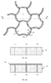
- Structure 2 is a cellular structure as illustrated, for example, in figure 3 , and of which a method of realization will be explained in detail below.
- the interface between the stress generating structure and the substrate is limited to regions where the walls of the cells are in contact with the substrate, so that the stress generating structure is locally secured to the substrate.
- a heat treatment is applied at a temperature adapted to cause deformation of the structure 2 in both dimensions of a plane parallel to the surface of the substrate 1.
- a temperature between 20 and 500 ° C is generally sufficient to cause the deformation of the structure.
- the temperature is also chosen according to the nature of the possible adhesive allowing the fastening of the structure to the substrate, so as not to degrade.
- the adhesive is an epoxy adhesive
- a temperature lower than 300 ° C. is preferably applied.
- this deformation generates a stress in the substrate that is greater than the mechanical strength of the substrate material, which leads to its cleavage along a plane C, parallel to the surface of the substrate, located at a certain depth .
- the cleavage plane C defines a layer 1 'which can then be detached for future use, possibly applying a mechanical force to separate it from the rest of the substrate.
- the structure 2 is not intended to be reused, it can be destructively removed, for example by removal of mechanical and / or chemical material.
- the structure 2 is intended to be reused, in which case it is removed from the layer 1 'non-destructively (for example by an attack of the adhesive used to bond the structure to the substrate) and it is prepared (for example, by a light polishing) for a new use.
- the structure 2 is not dismounted from the layer 1 'that has been detached, in particular if it must fulfill a function during the subsequent use of the detached layer.
- the structure 2 can be conserved and serve as a support for a photovoltaic layer, with the advantage that its transparent structure makes it possible to have electrical contacts on the rear face of the photovoltaic layer.
- the structure 2 can also serve as a stiffener to the detached layer 1 ', in particular when it has a thickness too small to be self-supporting (ie manipulable in isolation), that is to say typically when its thickness is less than 50 micrometers.
- the remaining portion of the substrate may be prepared for joining with a new stress generating structure to detach an additional layer.
- the method thus makes it possible to cut, as and when the ingot, into a plurality of layers.
- a first advantage of this method is that the structure used allows a great freedom of choice in the definition of its coefficient of thermal expansion.
- the criteria for defining the coefficient of thermal expansion are not the only materials used, but also the shape and size of the cells.
- a second advantage is that the structure employed has a coefficient of thermal expansion much higher than the individual thermal expansion coefficients of the materials constituting it.
- heating at a lower temperature than in the prior art is sufficient to generate in the substrate a stronger stress than its mechanical strength.
- the substrate when it is silicon, it has, at room temperature, a fragile and brittle character (or "brittle" in the English terminology).
- this heat treatment at a lower temperature is more favorable to possible devices that are formed in or on the loose layer, since it does not risk damaging them or affecting their performance.
- the stress generating structure is a cellular structure comprising a plurality of cells 2 'whose walls 2 "are bimetals 2a, 2b perpendicular to the surface of the substrate 1.
- Each bimetal consists of a first material 2a having a first coefficient of thermal expansion and a second material 2b having a second coefficient of thermal expansion significantly different from the first.
- the cells are identical and are repeated in a pattern determined in a plane parallel to the surface of the substrate.
- the cells 2 have a shape adapted to be able to deform in two dimensions in a plane parallel to the surface of the substrate.
- the cells have a substantially hexagonal shape, with successively concave and convex walls, and where the material located on the inner side of the cell is alternately the material 2a and the material 2b.
- FIGS. 4A to 4E are views according to the AA section presented at figure 3 .
- said layer is a 50 ⁇ m thick silicon layer.
- a deep engraving is used to create trenches T1, T2, T3 whose path defines the walls of the cells.
- the shape and dimensions of the cells will have been defined beforehand according to the required thermal expansion properties.
- the width of the trenches is, for example, 10 ⁇ m.
- the second material 2b is deposited after having deposited by vacuum evaporation or cathodic sputtering on the walls of the trenches a so-called metal layer (for example ten nm of titanium).
- the second material is a metal (such as aluminum or silver) which has a coefficient of thermal expansion greater than that of silicon.
- This deposition operation has the effect of filling the trenches T1, T2, T3 of the second material 2b and also to cover the surface of the first material 2a with a layer of the second material 2b.
- a thermal annealing at low temperature (that is to say typically of the order of 200 ° C. for aluminum) is carried out under a neutral atmosphere to densify the metal thus deposited.
- a resin mask 4 is deposited on the layer of the first material 2a.
- This mask is deposited selectively so as to cover the portions of the first material 2a that it is desired to preserve in the final cell structure 2.
- Said portions are adjacent to the trenches filled with the second material 2b, in order to form bimetals therewith.
- Their width is typically of the order of 10 microns.
- the resin mask is intended to protect the first material 2a adjacent to the second material 2b during the etching step that follows.
- etching of the first material 2a not protected by the mask 4 said etching being selective with respect to the second material 2b.
- the mask 4 is removed.
- Said structure is then secured to the surface of the substrate 1 by any suitable method of bonding.
- the structure is manufactured independently of the substrate and then secured to it.
- the layer of the first material 2a can be deposited on the surface of the substrate 1 by sputtering (or “sputtering” according to the English terminology), or preferably by chemical vapor deposition (or CVD, acronym of the term Anglo-Saxon “Chemical Vapor Deposition”) or by an electrochemical method, before proceeding to the etching that will form the cell structure.
- the surface of the substrate Prior to the bonding of the cellular structure or the deposition of the first material 2a from which the cellular structure will be formed, it is advantageous to prepare the surface of the substrate in order to promote the bonding with the stress-generating structure and / or to protect it possible contamination by the materials constituting the structure generating constraints.
- a protective layer of silicon oxide having a thickness of the order of 500 nanometers, deposited by a CVD technique or formed by thermal oxidation if the substrate is made of silicon can be formed.
- titanium bonding layer by a so-called “flash” evaporation step over a thickness of 100 to 300 Angstroms on said oxide layer to promote bonding with the metal of the stress-generating structure .
- the surface of the substrate is no longer flat and adapted to the fastening with the stress generating structure.
- a layer of SiO 2 is then deposited on the surface until the height of the devices is exceeded, and then it is planarized, for example by polishing, in order to join the stress generating structure.
- the figure 3 illustrates a view from above (that is to say in a direction perpendicular to the surface of the substrate 1) of the substrate-structure obtained cell structure.
- the second bimetallic material 2b extends further than the first material because of its higher coefficient of thermal expansion, which generates a tension and the walls of each cell 2 'are stretched. to become substantially straight.
- the elongation results in the application of a constraint inside the substrate, which leads to its cleavage.
- each bimetallic strip 2a, 2b exerts a discrete stress on the substrate of which it is integral, and all the discrete stresses thus exerted combine to generate a global stress whose intensity is greater than the mechanical strength of the substrate material in the cleavage plane C.
- the materials constituting the bimetallic strip must have the widest possible expansion coefficients.
- a ratio of about 2 or more between the thermal expansion coefficients of the two materials is desirable.
- one of the bimetal materials is silicon (whose CTE at 25 ° C. is of the order of 4.6 ⁇ 10 -6 K -1 )
- the other material is advantageously chosen from silver (CTE of the order of 18.10 -6 K -1 ), aluminum (CTE of the order of 23.10 -6 K -1 ), or even copper (CTE of the order of 16.5.10 -6 K -1 ) .
- SiO 2 silicon oxide
- Si x N y silicon nitride
- germanium CTE of the order of 6.1 ⁇ 10 -6 K -1
- metals mentioned above or still iron CTE of the order of 11.8 10 -6 K -1
- a material with a negative coefficient of thermal expansion such as zirconium tungstate ZrW 2 O 8 ) associated with a material with a coefficient of positive thermal expansion (for example 'money).
- bimetal is that it is not necessary to heat it strongly to obtain a large deformation, which makes it particularly suitable for the cleavage of silicon in a temperature range below 500 ° C, in which presents a fragile character (or "brittle").
- first and second materials forming the bimetallic strip are respectively a material having a high coefficient of positive thermal expansion (such as silver) and a material negative coefficient of thermal expansion, separated by a third material such as silicon.
- Silicon which has a median coefficient of thermal expansion, gives stability and mechanical strength to such a structure.
- a cell structure can be formed with tri-leaf walls in which the first and second bimetallic material are separated by a vacuum blade.
- the stress generating structure is also adapted to deform under the effect of a magnetic field.
- one of the materials constituting the bimetallic strip is a magnetostrictive material while having a coefficient of thermal expansion significantly different from that of the other material constituting the bimetal.
- the magnetostrictive material is chosen from materials having a percentage of elongation greater than 0.02% in absolute value and preferably a material whose magnetostriction is "giant" that is to say having a magnetostriction coefficient greater than 50 ppm in absolute value.
- An example of a magnetostrictive material well suited for the implementation of the invention is of Terfenol-D, which is an alloy of iron and rare earths, whose formula is Tb 0.3 Dy 0 7 Fe 19 and can be used in polycrystalline or amorphous form.
- the magnetostriction coefficient is different for each form (crystalline or amorphous) but remains greater than 50 ppm.
- the other material of the bimetallic strip is then typically silicon, SiC or germanium.
- the cell structure can be manufactured by the same method as that described above.
- the structure thus formed is capable of deforming under the combined effect of the temperature (which can then be lower than in the case where it uses only the heat treatment to cause its deformation) and a magnetic field .
- the relative increase in the dimensions of the structure may be 10 to 100 times greater than the relative elongation of the magnetostrictive material.
- This amplification coefficient depends on the geometric design of the cells and their network arrangement.
- This amplification allows for a given expansion or contraction of the stress-generating structure, the application of a lower heat treatment, compatible with the presence of electronic devices that are very sensitive to the temperature in or on the substrate, compared to the previous embodiment where the structure expands or contracts only under the effect of the temperature
- the applied temperature must remain significantly lower than the Curie temperature Tc of the magnetostrictive material, so as not to alter the magnetic properties of the stress generating structure.
- the Curie temperature is 380 ° C, so that the heat treatment will not be applied at a temperature of more than 350 ° C, and preferably will be applied at a temperature below 300 ° C .
- the Curie temperature is between 630 and 710 ° C; the heat treatment will therefore be applied at a temperature preferably below 600 ° C.
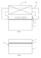
- the magnetic field is applied by means of a magnetic circuit 5a surrounding the stress generating structure 2, said magnetic circuit being surrounded by a conductive coil 5b.
- this device As represented by the horizontal arrow, this device generates an induction parallel to the surface of the substrate.
- the applied magnetic field is preferably static and oriented parallel to the largest dimension of the substrate.
- the magnetic field is applied in the form of a combination of variable fields creating a rotating induction in the plane of the substrate, in order to cause a dilation in both dimensions of the stress generating structure.
- the necessary magnetic induction is typically between 0.1 and 1 Tesla.
- An advantage of the magnetic treatment is that it can be produced without contact with the stress generating structure or the substrate to be cleaved, which facilitates its implementation.
- the substrate can be weakened before the application of the heat treatment (and, where appropriate, the magnetic field), in order to facilitate its cleavage.
- a fragile zone 10 is formed in the substrate in a plane corresponding to the cleavage plane.
- the embrittlement can result from implantation of ionic species combined or not with heat treatments, which can result in the creation of pores and / or microbubbles in a plane corresponding to the cleavage plane.
- the implanted species dose is approximately 10-fold less than required for a Smart Cut TM fracture.
- the H + ion implantation dose for a Smart Cut TM fracture at 20 micrometers in silicon is approximately 10 17 atoms / cm 2
- the dose required for pre-fragilization according to the The invention is in the range of from 5 ⁇ 10 15 to 10 16 atoms / cm 2 .
- Said embrittlement treatment can also be performed during the development of the substrate.
- an embrittlement zone may consist of an epitaxial layer 2 ⁇ m thick of Si x -Ge 1-x (where 0 ⁇ x ⁇ 0.8) on a silicon substrate, this layer having a percentage of maximum germanium (up to 20%) at the center of the layer and decreasing to about 5% when approaching the lower and upper interfaces.
- germanium gradient in the Si x -Ge 1-x layer is chosen to allow epitaxial growth with sufficient crystalline quality (ie low dislocation density, absence of crack) of the overlying Si layer which is destined to be detached later.
- This concentration gradient makes it possible in fact to continuously adapt the mesh parameter of Si x -Ge 1-x to that of the underlying silicon without creating relaxation of stresses in the layer by the formation of dislocations.
- the Si x -Ge 1-x layer is mechanically more fragile than the under- and overlying layers of silicon and the cleavage will occur at its level.
- cleavage can be facilitated by providing a breakthrough in the substrate at the desired depth.
- the incipient fracture may be in the form of an indentation 11 (typically a few tens of micrometers deep) made on a lateral face of the substrate 1, at the depth corresponding substantially to the depth at which the generating structure constraints must induce the fracture (plane C mentioned below).
- Such a primer allows, in a depth range where the stress is very high, to precisely choose the location of the rupture in the substrate.
- the initiation of rupture can be performed mechanically, using a cutting tool, and / or chemical.
- a selective pyrocatechol etching is carried out at the periphery of the layer. of P + doped silicon to form a notch.
- the depth of this cut depends on the duration of the chemical attack.
- a cellular structure is formed as illustrated in plan view at the figure 3 .
- the walls of the cells are formed of a bimetallic silicon 2a / silver 2b.
- the width of the silicon and silver blades is about 10 micrometers.
- the thickness (in a direction perpendicular to the surface of the substrate) of the cell structure is about 40 microns.
- Each cell is inscribed in a circle 100 micrometers in diameter, each side of the cell having a length of about 50 microns and being curved with an arrow of about 10 microns.
- a protective layer of oxide is preferably formed on the surface of the silicon substrate before bonding the structure to the substrate, said oxide layer being removed after cleavage of the substrate and removal of the structure of the loose layer.
- This cell structure is bonded to the surface of the substrate by a molecular adhesion process capable of providing a high adhesion energy density from ambient temperature, for example an adhesion process with surface preparation by plasma treatment. It is known that this type of treatment makes it possible to obtain adhesion energy densities of several hundred mJ / m 2 .
- the adhesion process that is to say the increase of the adhesion energy, will then be carried out by increasing the temperature of the assembly according to a sufficiently slow temperature ramp as a function of time (typically 5 ° C. / mn) so that the adhesion process is completely completed before a possible parasitic effect of deformation of the cellular structure can not be exerted substantially on the bonding interface.
- the whole is then heated to a temperature of about 450 ° C.
- This temperature is sufficiently moderate that the bimetal silver does not contaminate the substrate through the aforementioned protective layer.
- the silver blade elongates more than the silicon blade, which causes the curved walls to stretch until substantially rectilinear walls.
- This deformation generates a constraint in the silicon substrate which makes it possible to cleave it to a depth of between 50 and 100 micrometers.
- the cell structure may be fabricated with straight walls for each cell, said walls being curved under the effect of heat treatment.
Abstract
Description
La présente invention concerne un procédé de clivage d'un substrat en vue du détachement d'une couche dudit substrat.The present invention relates to a method of cleaving a substrate for detaching a layer of said substrate.
Le détachement de couches épaisses d'un substrat se pose particulièrement dans l'industrie des semi-conducteurs.The detachment of thick layers of a substrate is particularly relevant in the semiconductor industry.
Différents procédés de détachement sont déjà connus et largement employés.Different methods of detachment are already known and widely used.
Certains procédés comprennent la formation, à l'intérieur du substrat, d'une zone de fragilisation délimitant la couche à détacher, puis l'application au substrat ou à la zone de fragilisation, de contraintes visant à provoquer le clivage du substrat suivant la zone de fragilisation. Ces contraintes peuvent être de nature thermique et/ou mécanique, etc.Some methods include the formation, inside the substrate, of an embrittlement zone delimiting the layer to be detached, and then the application to the substrate or to the embrittlement zone of stresses intended to cause the cleavage of the substrate according to the zone. fragilization. These constraints may be of a thermal and / or mechanical nature, etc.
Ainsi, le procédé Smart Cut ™ comprend la formation, dans un substrat donneur, d'une zone de fragilisation par implantation d'espèces atomiques, délimitant la couche à transférer, suivie du collage du substrat donneur sur un substrat receveur et le clivage du substrat donneur suivant la zone de fragilisation, conduisant au report de la couche sur le substrat receveur.Thus, the Smart Cut ™ process comprises the formation, in a donor substrate, of an embrittlement zone by implantation of atomic species, delimiting the layer to be transferred, followed by bonding of the donor substrate to a receiving substrate and cleavage of the substrate donor following the zone of weakening, leading to the transfer of the layer on the receiving substrate.
Cependant, ce procédé est plus approprié au transfert de couches minces, c'est-à-dire d'épaisseur typiquement inférieure au micromètre.However, this method is more suitable for the transfer of thin layers, that is to say of thickness typically less than one micrometer.
En effet, les implanteurs à vocation industrielle présentent à l'heure actuelle une énergie jusqu'à 200 keV, ce qui permet d'atteindre une profondeur d'implantation pouvant atteindre 2 micromètres environ, selon les matériaux et les espèces ioniques implantées.In fact, industrial implants presently have an energy up to 200 keV, which allows to reach an implantation depth of up to 2 micrometers, depending on the materials and ionic species implanted.
Par exemple, une implantation d'ions H+ dans du silicium permet d'atteindre une profondeur de 1,8 micromètres environ, mais la profondeur atteinte sera plus faible dans du GaN qui est plus dense.For example, an implantation of H + ions in silicon makes it possible to reach a depth of about 1.8 micrometers, but the depth reached will be lower in GaN which is denser.
Il existe des implanteurs à haute énergie, c'est-à-dire de l'ordre de 1 MeV, qui permettraient d'atteindre une profondeur jusqu'à 20 micromètres, mais le procédé ne serait pas économiquement viable en raison du coût élevé de ces machines.There are high-energy implementers, that is to say of the order of 1 MeV, which would allow to reach a depth up to 20 micrometers, but the process would not be economically viable because of the high cost of these machines.
La demande de brevet
L'application d'une contrainte thermique au substrat recouvert de la couche métallique engendre une contrainte de clivage dans le substrat, à une profondeur correspondant à l'épaisseur de la couche que l'on souhaite détacher, conduisant au clivage du substrat et au détachement de la couche désirée.The application of a thermal stress to the substrate covered with the metal layer generates a cleavage stress in the substrate, at a depth corresponding to the thickness of the layer that is to be detached, leading to cleavage of the substrate and detachment of the desired layer.
L'obtention de la contrainte de clivage est liée à la différence de coefficient de dilatation thermique (CTE, acronyme du terme anglo-saxon « Coefficient of Thermal Expansion ») entre le matériau de la couche métallique et le matériau du substrat.Obtaining the cleavage constraint is related to the difference in thermal expansion coefficient (CTE), which is the acronym for the term "Coefficient of Thermal Expansion", between the material of the metal layer and the material of the substrate.
Ainsi, par exemple, le coefficient de dilatation thermique du silicium est de 4,6.10-6 K-1 tandis que celui de l'argent est de 20.10-6 K-1 et celui de l'aluminium de 24.10-6 K-1.Thus, for example, the coefficient of thermal expansion of silicon is 4.6 × 10 -6 K -1 while that of silver is 20 × 10 -6 K -1 and that of aluminum 24 × 10 -6 K -1 .
Cependant, le dépôt de métaux sur le substrat de silicium risque de contaminer la couche semi-conductrice, ce qui est préjudiciable au fonctionnement du dispositif fabriqué à partir de cette couche.However, the deposition of metals on the silicon substrate may contaminate the semiconductor layer, which is detrimental to the operation of the device made from this layer.
Par ailleurs, le coefficient de dilatation thermique de la couche génératrice de contraintes est dépendant de la nature du matériau employé.Moreover, the coefficient of thermal expansion of the stress-generating layer is dependent on the nature of the material used.
Il en résulte que l'homme du métier est nécessairement limité dans la définition du procédé par les matériaux disponibles sur le marché.As a result, those skilled in the art are necessarily limited in the definition of the process by the materials available on the market.
En particulier, il ne peut pas forcément former une couche génératrice de contraintes présentant le coefficient de dilatation thermique souhaité.In particular, it can not necessarily form a stress generating layer having the desired coefficient of thermal expansion.
Enfin, pour provoquer la dilatation de la couche génératrice de contraintes selon le procédé précité, il est généralement nécessaire de la chauffer à une température élevée, c'est-à-dire typiquement de l'ordre de 800°C.Finally, to cause the expansion of the stress-generating layer according to the aforementioned method, it is generally necessary to heat it at an elevated temperature, that is to say typically of the order of 800 ° C.
Cependant, le silicium présente, dans cette gamme de température, un caractère ductile, ce qui est défavorable à l'obtention du clivage du substrat.However, the silicon has, in this temperature range, a ductile character, which is unfavorable to obtaining the cleavage of the substrate.
L'un des buts de la présente invention est donc de procurer un procédé de détachement d'une couche d'un substrat présentant une épaisseur typiquement comprise entre 1 et 100 micromètres qui évite les inconvénients des méthodes évoquées plus haut.One of the aims of the present invention is therefore to provide a method of detaching a layer of a substrate having a thickness typically between 1 and 100 microns which avoids the disadvantages of the methods mentioned above.
Plus précisément, l'invention vise à permettre le détachement d'une couche d'un substrat sans risquer de contaminer le matériau du substrat.More specifically, the invention aims to allow the detachment of a layer of a substrate without the risk of contaminating the substrate material.
L'invention a également pour but de limiter la température nécessaire pour procurer le clivage du substrat.The invention also aims to limit the temperature necessary to provide cleavage of the substrate.
En outre, l'invention doit également procurer une plus grande liberté de choix dans le coefficient de dilatation thermique de la structure génératrice de contraintes, en vue notamment d'optimiser le clivage du substrat.In addition, the invention must also provide greater freedom of choice in the thermal expansion coefficient of the stress generating structure, in particular to optimize the cleavage of the substrate.
Conformément à l'invention, il est proposé un procédé de clivage d'un substrat en vue d'en détacher une couche, comprenant les étapes successives suivantes :
- (i) la formation d'une structure dite génératrice de contraintes, solidaire localement de la surface du substrat, ladite structure génératrice de contraintes étant une structure cellulaire dont les parois des cellules sont perpendiculaires à la surface du substrat et sont composées d'au moins deux matériaux présentant des coefficients de dilatation thermique différents agencés pour permettre une déformation desdites parois sous l'effet d'un traitement thermique, de sorte que ladite structure est adaptée pour se dilater ou se contracter dans un plan parallèle à la surface du substrat sous l'effet dudit traitement thermique,
- (ii) l'application à ladite structure d'un traitement thermique adapté pour provoquer la dilatation ou la contraction de ladite structure de manière à générer dans le substrat une pluralité de contraintes locales dont la combinaison génère une contrainte supérieure à la résistance mécanique du substrat dans un plan de clivage parallèle à la surface du substrat définissant la couche à détacher, ladite contrainte conduisant au clivage du substrat selon ledit plan.
- (i) forming a so-called stress generating structure, locally secured to the surface of the substrate, said stress generating structure being a cellular structure whose cell walls are perpendicular to the surface of the substrate and are composed of at least two materials having different thermal expansion coefficients arranged to allow a deformation of said walls under the effect of heat treatment, so that said structure is adapted to expand or contract in a plane parallel to the surface of the substrate under the effect of said heat treatment,
- (ii) the application to said structure of a thermal treatment adapted to cause the expansion or contraction of said structure so as to generate in the substrate a plurality of local stresses whose combination generates a stress greater than the mechanical strength of the substrate in a cleavage plane parallel to the surface of the substrate defining the layer to be detached, said stress leading to the cleavage of the substrate along said plane.
Par « solidaire » on entend dans le présent texte que la force de cohésion entre la structure génératrice de contraintes et la surface du substrat doit être supérieure aux contraintes exercées lors de la dilatation ou la contraction de la structure, pour qu'il n'y ait pas de rupture à l'interface et que les contraintes engendrées par la déformation de la structure soient transmises au substrat pour permettre son clivage.By "solidary" is meant in the present text that the cohesive force between the stress generating structure and the surface of the substrate must be greater than the stresses exerted during the expansion or contraction of the structure, so that There is no break at the interface and the stresses generated by the deformation of the structure are transmitted to the substrate to allow its cleavage.
Par « localement » on entend que la liaison entre la structure génératrice de contraintes et le substrat n'existe que dans des régions déterminées de la surface du substrat, et non en tout point de la surface du substrat.By "locally" is meant that the bond between the stress generating structure and the substrate exists only in specific regions of the surface of the substrate, and not at any point on the surface of the substrate.
De manière particulièrement avantageuse, les au moins deux matériaux présentant des coefficients de dilatation thermique différents agencés pour permettre une déformation desdites parois sous l'effet dudit traitement thermique, procurent un effet bilame.Particularly advantageously, the at least two materials having different thermal expansion coefficients arranged to allow deformation of said walls under the effect of said heat treatment, provide a bimetallic effect.
Par « procurer un effet bilame » on entend dans le présent texte le fait que deux matériaux présentant des coefficients de dilatation thermique différents sont agencés de manière solidaire l'un par rapport à l'autre de telle sorte que l'ensemble se déforme en dilatation ou contraction sous l'effet d'un traitement thermique et, éventuellement, d'un champ magnétique si l'un des matériaux est en outre magnétostrictif.By "providing a bimetallic effect" is meant in the present text the fact that two materials having different coefficients of thermal expansion are arranged integrally with respect to each other so that the whole is deformed in expansion or contraction under the effect of a heat treatment and possibly a magnetic field if one of the materials is further magnetostrictive.
Selon les modes de réalisation décrits plus bas, les deux matériaux peuvent se présenter sous la forme de deux lames accolées solidaires l'une de l'autre, l'interface entre les deux matériaux présentant une surface sensiblement perpendiculaire à la surface du substrat.According to the embodiments described below, the two materials may be in the form of two contiguous blades integral with each other, the interface between the two materials having a surface substantially perpendicular to the surface of the substrate.
Par extension, on entend aussi par « bilame » tout agencement de deux ou plus de deux matériaux présentant des coefficients de dilatation différents, sous forme de multi-lames accolées les unes aux autres de façon solidaire et dont les interfaces entre chacun des matériaux se présenteraient sous la forme d'une surface sensiblement perpendiculaire à la surface du substrat.By extension, "bimetallic" is also understood to mean any arrangement of two or more materials having different coefficients of expansion, in the form of multi-blades contiguous to each other in solidarity and whose interfaces between each of the materials would occur. in the form of a surface substantially perpendicular to the surface of the substrate.
Cette définition inclut donc notamment un trilame composé par exemple d'une lame centrale de silicium entourée respectivement d'une lame d'un matériau à CTE positif et d'une lame d'un matériau à CTE négatif.This definition therefore includes, in particular, a trilame composed, for example, of a central silicon strip surrounded respectively by a plate of a positive CTE material and a plate of a CTE negative material.
Selon un mode de réalisation de l'invention, les parois des cellules sont des bilames formés d'un premier et d'un deuxième matériau qui présentent des coefficients de dilatation thermique qui diffèrent d'un rapport d'au moins 2.According to one embodiment of the invention, the walls of the cells are bimetals formed of a first and a second material which have thermal expansion coefficients which differ by a ratio of at least 2.
Par exemple, la structure génératrice de contraintes comprend des bilames formés des couples de matériaux suivants : Si/Ag, Si/Al, Si/Cu, Si/SiO2 Ge/Ag, Ge/Al, Ge/Cu, Ge/Fe, Ge/SiO2, saphir/Ag, saphir/Al, saphir/Cu, et/ou saphir/SiO2 For example, the stress generating structure comprises bimetals formed from the following pairs of materials: Si / Ag, Si / Al, Si / Cu, Si / SiO 2 Ge / Ag, Ge / Al, Ge / Cu, Ge / Fe, Ge / SiO 2 , sapphire / Ag, sapphire / Al, sapphire / Cu, and / or sapphire / SiO 2
Selon un autre mode de réalisation, les parois des cellules sont des bilames formés d'un premier et d'un deuxième matériau dont l'un présente un coefficient de dilatation thermique positif et l'autre un coefficient de dilatation thermique négatif.According to another embodiment, the walls of the cells are bimetals formed of a first and a second material, one of which has a coefficient of positive thermal expansion and the other a coefficient of negative thermal expansion.
Par exemple, lesdits bilames sont formés des couples de matériaux suivants : Si/ZrW2O8, Cu/ZrW2O8, Al/ZrW2O8, et/ou Ag/ ZrW2O8.For example, said bimetallic strips are formed from the following pairs of materials: Si / ZrW 2 O 8 , Cu / ZrW 2 O 8 , Al / ZrW 2 O 8 , and / or Ag / ZrW 2 O 8 .
Selon un autre mode de réalisation, le premier et le deuxième matériau du bilame sont séparés par du vide ou par une lame d'un troisième matériau, en particulier le bilame est formé par le couple Ag/ZrW2O8 et la lame du troisième matériau est du silicium.According to another embodiment, the first and second material of the bimetallic strip are separated by a vacuum or by a blade of a third material, in particular the bimetallic strip is formed by the pair Ag / ZrW 2 O 8 and the blade of the third material is silicon.
De manière particulièrement avantageuse, le traitement thermique de l'étape (ii) est appliqué à une température comprise entre 20 et 500°C.Particularly advantageously, the heat treatment of step (ii) is applied at a temperature between 20 and 500 ° C.
Selon une forme d'exécution particulièrement avantageuse de l'invention, la structure génératrice de contraintes est en outre adaptée pour se dilater ou se contracter dans un plan parallèle à la surface du substrat sous l'action d'un champ magnétique.According to a particularly advantageous embodiment of the invention, the stress generating structure is further adapted to expand or contract in a plane parallel to the surface of the substrate under the action of a magnetic field.
A cet effet, ladite structure génératrice de contraintes est une structure cellulaire dont les parois des cellules sont perpendiculaires à la surface du substrat et sont composées d'au moins deux matériaux présentant des coefficients de dilatation thermique différents agencés pour permettre une déformation desdites parois sous l'effet dudit traitement thermique, et l'un desdits matériaux est un matériau magnétostrictif.For this purpose, said stress-generating structure is a cellular structure whose cell walls are perpendicular to the surface of the substrate and are composed of at least two materials having different thermal expansion coefficients arranged to allow deformation of said walls under the substrate. effect of said heat treatment, and one of said materials is a magnetostrictive material.
De manière préférée, le matériau magnétostrictif est un alliage de terre rare et de fer, tel que Terfenol-D, SmFe2, DyFe2 ou TbFe2, et l'autre matériau est du silicium, du SiC ou du germanium.Preferably, the magnetostrictive material is an alloy of rare earth and iron, such as Terfenol-D, SmFe 2 , DyFe 2 or TbFe 2 , and the other material is silicon, SiC or germanium.
Dans ce cas, le traitement thermique est préférentiellement appliqué à une température inférieure à la température de Curie du matériau magnétostrictif et l'on applique en outre à ladite structure génératrice de contraintes un champ magnétique adapté pour provoquer une élongation ou une rétraction dudit matériau magnétostrictif.In this case, the heat treatment is preferably applied at a temperature below the Curie temperature of the magnetostrictive material and a magnetic field adapted to cause an elongation or retraction of said magnetostrictive material is also applied to said stress generating structure.
Si le substrat présente une forme allongée, le champ magnétique appliqué est de préférence statique et orienté parallèlement à la plus grande dimension du substrat.If the substrate has an elongate shape, the applied magnetic field is preferably static and oriented parallel to the largest dimension of the substrate.
Si le substrat présente une forme de disque, le champ magnétique appliqué est tournant de manière à provoquer une dilatation ou une contraction de la structure selon deux directions perpendiculaires dans un plan parallèle à la surface du substrat.If the substrate has a disc shape, the applied magnetic field is rotated to cause expansion or contraction of the structure in two perpendicular directions in a plane parallel to the surface of the substrate.
Selon un mode particulier de réalisation de l'invention, la structure génératrice de contraintes est rendue solidaire de la surface du substrat par une couche de collage.According to a particular embodiment of the invention, the stress-generating structure is made integral with the surface of the substrate by a bonding layer.
La structure génératrice de contraintes peut être fabriquée avant d'être rendue solidaire du substrat par gravure de tranchées dans une couche du premier matériau, remplissage desdites tranchées par le deuxième matériau, masquage des portions de la couche du premier matériau destinées à la formation du bilame et gravure sélective de ladite couche pour retirer les portions non masquées du premier matériau.The stress generating structure may be fabricated before being secured to the substrate by etching trenches in a layer of the first material, filling said trenches with the second material, masking the portions of the layer of the first material intended for the formation of the bimetal and selectively etching said layer to remove the unmasked portions of the first material.
De manière alternative, la structure génératrice de contraintes est rendue solidaire du substrat par dépôt d'une couche du premier matériau sur la surface du substrat, suivi par la gravure des tranchées dans ladite couche, remplissage desdites tranchées par le deuxième matériau, masquage des portions de la couche du premier matériau destinées à la formation du bilame et gravure sélective de ladite couche pour retirer les portions non masquées du premier matériau.Alternatively, the stress-generating structure is made integral with the substrate by depositing a layer of the first material on the surface of the substrate, followed by etching the trenches in said layer, filling said trenches with the second material, masking the portions. of the layer of the first material for forming the bimetal and selectively etching said layer to remove unmasked portions of the first material.
L'épaisseur de la couche détachée du substrat est comprise entre 1 et 100 micromètres, de préférence entre 30 et 70 micromètres, de préférence environ 50 micromètres.The thickness of the layer detached from the substrate is between 1 and 100 microns, preferably between 30 and 70 microns, preferably about 50 microns.
Il existe typiquement un rapport compris entre 0,1 et 10 entre l'épaisseur de la couche à détacher et l'épaisseur de la structure génératrice de contraintes.There is typically a ratio between 0.1 and 10 between the thickness of the layer to be detached and the thickness of the stress generating structure.
Selon un mode particulier de réalisation, on forme dans le substrat, avant l'étape (ii), une zone fragile de manière à procurer le clivage selon ladite zone fragile.According to a particular embodiment, a fragile zone is formed in the substrate before step (ii) so as to provide cleavage along said fragile zone.
Par exemple, ladite zone fragile est formée par implantation d'espèces ioniques dans le substrat à la profondeur du plan de clivage, avec une dose comprise entre 5.1015 et 1016 atomes/cm2 . For example, said frangible zone is formed by implantation of ionic species into the substrate to the depth of the cleave plane with a dose of between 5.10 15 and 10 16 atoms / cm 2.
De manière alternative, le substrat et la couche à détacher sont en silicium et la zone fragile est une couche de SixGe1-x avec 0<x<0,8 dans laquelle la proportion de germanium évolue graduellement entre une valeur minimale aux interfaces et une valeur maximale au centre.Alternatively, the substrate and the layer to be detached are made of silicon and the fragile zone is a layer of Si x Ge 1-x with 0 <x <0.8 in which the proportion of germanium evolves gradually between a minimum value at the interfaces and a maximum value at the center.
Selon une variante de réalisation, on réalise, avant l'étape (ii), une amorce de rupture dans le substrat à la profondeur du plan de clivage.According to an alternative embodiment, before step (ii), a rupture primer is produced in the substrate at the depth of the cleavage plane.
Avant l'étape (i), on peut former dans ou sur la couche à détacher du substrat des dispositifs électroniques pour applications optoélectroniques et/ou photovoltaïques, et/ou de puissance et/ou des circuits électroniques et/ou des microsystèmes.Before step (i), electronic devices for optoelectronic and / or photovoltaic and / or power applications and / or electronic circuits and / or microsystems may be formed in or on the layer to be detached from the substrate.
La structure génératrice de contraintes peut être retirée de la couche après que celle-ci a été détachée du substrat.The stress generating structure can be removed from the layer after it has been detached from the substrate.
Par exemple, la structure génératrice de contraintes peut être recyclée après son retrait de la couche détachée en vue d'une nouvelle utilisation pour cliver un substrat.For example, the stress generating structure may be recycled after removal from the loose layer for further use in cleaving a substrate.
Le substrat est typiquement en un matériau semi-conducteur.The substrate is typically a semiconductor material.
Selon une forme d'exécution particulière de l'invention, le substrat est un lingot d'un matériau semi-conducteur et l'on applique les étapes (i) et (ii) à plusieurs reprises pour détacher successivement une pluralité de couches dudit substrat.According to one particular embodiment of the invention, the substrate is an ingot of a semiconductor material and steps (i) and (ii) are applied several times to successively detach a plurality of layers of said substrate. .
Un autre objet de l'invention concerne un ensemble comprenant un substrat et une structure dite génératrice de contraintes solidaire de la surface dudit substrat, caractérisé en ce que ladite structure génératrice de contraintes est une structure cellulaire dont les parois des cellules sont perpendiculaires à la surface du substrat et sont composées d'au moins deux matériaux présentant des coefficients de dilatation thermique différents agencés pour permettre une déformation desdites parois sous l'effet d'un traitement thermique.Another subject of the invention relates to an assembly comprising a substrate and a so-called stress-generating structure integral with the surface of said substrate, characterized in that said stress-generating structure is a cellular structure whose cell walls are perpendicular to the surface. of the substrate and are composed of at least two materials having different thermal expansion coefficients arranged to allow deformation of said walls under the effect of a heat treatment.
Enfin, un autre objet de l'invention concerne un dispositif semi-conducteur pour applications photovoltaïques, optoélectroniques ou en électronique, comprenant une couche en matériau semi-conducteur et un support qui est une structure cellulaire, solidaire de la surface de ladite couche, dont les parois des cellules sont perpendiculaires à la surface de la couche et sont composées d'au moins deux matériaux présentant des coefficients de dilatation thermique différents agencés pour permettre une déformation desdites parois sous l'effet d'un traitement thermique.Finally, another object of the invention relates to a semiconductor device for photovoltaic, optoelectronic or electronic applications, comprising a layer of semiconductor material and a support which is a cellular structure, integral with the surface of said layer, of which the walls of the cells are perpendicular to the surface of the layer and are composed of at least two materials having different coefficients of thermal expansion arranged to allow deformation of said walls under the effect of a heat treatment.
D'autres caractéristiques et avantages de l'invention ressortiront de la description détaillée qui va suivre, en référence aux dessins annexés sur lesquels :
- la
figure 1 est une vue en coupe d'un substrat et d'une structure génératrice de contrainte selon l'invention, - la
figure 2 est une vue en coupe du substrat de lafigure 1 clivé et de ladite structure, - la
figure 3 est une vue de dessus d'un mode particulier de l'invention, dans lequel la structure est formée d'une pluralité de cellules dont les parois sont des bilames, - les
figures 4A à 4E illustrent des étapes du procédé de réalisation de la structure de lafigure 3 , - la
figure 5 est une vue en coupe schématisant l'application d'un champ magnétique à la structure génératrice de contraintes, - la
figure 6 est une vue en coupe d'un mode de réalisation de l'invention dans lequel le substrat à cliver a été pré-fragilisé, - la
figure 7 est une vue en coupe d'une variante dans laquelle une amorce de rupture a été réalisée dans le substrat à cliver.
- the
figure 1 is a sectional view of a substrate and a strain generating structure according to the invention, - the
figure 2 is a sectional view of the substrate of thefigure 1 cleaved and of said structure, - the
figure 3 is a view from above of a particular embodiment of the invention, in which the structure is formed of a plurality of cells whose walls are bimetallic, - the
FIGS. 4A to 4E illustrate steps in the process of realizing the structure of thefigure 3 , - the
figure 5 is a sectional view schematizing the application of a magnetic field to the stress generating structure, - the
figure 6 is a sectional view of an embodiment of the invention in which the substrate to be cleaved has been pre-weakened, - the
figure 7 is a sectional view of a variant in which a rupture primer has been made in the substrate to be cleaved.
Pour faciliter l'illustration, les rapports d'épaisseurs des différentes couches n'ont pas nécessairement été respectés.For ease of illustration, the thickness ratios of the different layers have not necessarily been respected.
En référence à la
Le substrat peut être tout matériau (semi conducteur, métal, etc.), quelle que soit sa structure cristalline (monocristallin, poly-cristallin, amorphe).The substrate may be any material (semiconductor, metal, etc.), regardless of its crystalline structure (monocrystalline, polycrystalline, amorphous).
De manière préférée, le substrat est en un matériau semi-conducteur tel que Si, SiC, Ge, un substrat de type IV, II/VI ou III/V tel que GaN, InGaN, AsGa, InP et autres alliages binaires, ternaires, quaternaires de ces éléments.Preferably, the substrate is made of a semiconductor material such as Si, SiC, Ge, a type IV, II / VI or III / V substrate such as GaN, InGaN, AsGa, InP and other binary, ternary alloys. quaternaries of these elements.
Selon un mode particulier de réalisation, la couche qui doit être détachée du substrat est une couche active formée d'une pluralité de matériaux semi-conducteurs superposés et/ou elle comprend des dispositifs électroniques pour applications optoélectroniques (par exemple, LED, laser) et/ou photovoltaïques (tels que des cellules multi-jonctions pour le terrestre et le spatial) ; elle peut également comprendre des circuits électroniques, en particulier pour des applications de puissance, et/ou des microsystèmes.According to a particular embodiment, the layer to be detached from the substrate is an active layer formed of a plurality of superimposed semiconductor materials and / or it comprises electronic devices for optoelectronic applications (for example, LED, laser) and / or photovoltaic (such as multi-junction cells for terrestrial and spatial); it may also include electronic circuits, in particular for power applications, and / or microsystems.
Lesdits dispositifs sont formés dans ou sur la couche à détacher avant la solidarisation du substrat avec la structure génératrice de contraintes.Said devices are formed in or on the layer to be detached before bonding the substrate with the stress generating structure.
Cette structure doit être solidaire de la surface du substrat pour lui transmettre les contraintes qui vont conduire au clivage du substrat.This structure must be integral with the surface of the substrate to transmit the stresses that will lead to cleavage of the substrate.
On choisit donc un mode de liaison adapté entre la structure et le substrat.A suitable mode of connection is thus chosen between the structure and the substrate.
Selon les matériaux en présence, on peut procéder à un collage par adhésion moléculaire, par brasage, ou par un adhésif approprié, présentant notamment une bonne tenue à la température du traitement thermique qui va être mis en oeuvre pour conduire au clivage du substrat.According to the materials in the presence, it is possible to carry out a bonding by molecular adhesion, by soldering, or by an appropriate adhesive, having in particular a good resistance to the temperature of the heat treatment which will be used to lead to the cleavage of the substrate.
Lorsque la structure doit être retirée de la couche qui sera détachée du substrat, il est préférable de prévoir un adhésif permettant un collage réversible, c'est-à-dire qui permettra un démontage de la structure de manière non destructive.When the structure must be removed from the layer that will be detached from the substrate, it is preferable to provide an adhesive for reversible bonding, that is to say that will allow disassembly of the structure in a non-destructive manner.
Par exemple, l'adhésif employé est une colle époxy.For example, the adhesive used is an epoxy glue.
Une telle colle présente l'avantage d'être hydrolysable ; elle peut donc être éliminée par action de la vapeur d'eau à 100°C.Such a glue has the advantage of being hydrolyzable; it can therefore be removed by the action of water vapor at 100 ° C.
Dans le mode de réalisation illustré à la
Cependant, la couche de collage est optionnelle et, en fonction des matériaux considérés, on pourra procéder à un collage par adhésion moléculaire en mettant directement en contact la structure génératrice de contraintes avec la surface du substrat.However, the bonding layer is optional and, depending on the materials considered, it will be possible to carry out a molecular bonding bonding by directly contacting the stress-generating structure with the surface of the substrate.
La structure 2 est une structure cellulaire telle qu'illustrée par exemple à la
Les parois 2" des cellules 2' sont constituées par des bilames (voire des trilames) de matériaux présentant des coefficients de dilatation thermique significativement différents, lesdites parois étant perpendiculaires à la surface du substrat.The
Par « significativement différent », on entend qu'il existe par exemple un rapport d'environ 2 ou plus entre les coefficients de dilatation thermique des deux matériaux, ou que les coefficients de dilatation thermique des dits matériaux sont de signes opposés.By "significantly different" it is meant that there is for example a ratio of about 2 or more between the thermal expansion coefficients of the two materials, or that the coefficients of thermal expansion of said materials are of opposite signs.
L'interface entre la structure génératrice de contraintes et le substrat est limitée aux régions où les parois des cellules sont en contact avec le substrat, de sorte que la structure génératrice de contraintes est solidaire localement du substrat.The interface between the stress generating structure and the substrate is limited to regions where the walls of the cells are in contact with the substrate, so that the stress generating structure is locally secured to the substrate.
Pour provoquer le clivage du substrat, on applique un traitement thermique à une température adaptée pour provoquer une déformation de la structure 2 dans les deux dimensions d'un plan parallèle à la surface du substrat 1.To cause the cleavage of the substrate, a heat treatment is applied at a temperature adapted to cause deformation of the
En raison de la géométrie de la structure cellulaire qui lui procure un coefficient de dilatation thermique très élevé, une température comprise entre 20 et 500°C est généralement suffisante pour provoquer la déformation de la structure.Because of the geometry of the cellular structure which gives it a very high coefficient of thermal expansion, a temperature between 20 and 500 ° C is generally sufficient to cause the deformation of the structure.
La température est également choisie en fonction de la nature de l'éventuel adhésif permettant la solidarisation de la structure au substrat, afin de ne pas le dégrader.The temperature is also chosen according to the nature of the possible adhesive allowing the fastening of the structure to the substrate, so as not to degrade.
Ainsi, dans le cas où l'adhésif est une colle époxy, on applique de préférence une température inférieure à 300°C.Thus, in the case where the adhesive is an epoxy adhesive, a temperature lower than 300 ° C. is preferably applied.
La structure 2 étant solidaire du substrat 1, cette déformation engendre dans le substrat une contrainte supérieure à la résistance mécanique du matériau du substrat, ce qui conduit à son clivage selon un plan C, parallèle à la surface du substrat, situé à une certaine profondeur.As the
Plus le substrat est mince, plus il est souple et plus le clivage a lieu en profondeur dans le substrat.The thinner the substrate, the more flexible it is and the deeper the cleavage takes place in the substrate.
En revanche, un substrat plus épais donnera lieu à un clivage moins profond.On the other hand, a thicker substrate will give rise to a shallower cleavage.
Comme on peut le voir à la
Une fois la couche 1' détachée, on peut retirer la structure 2 qui a servi au clivage.Once the layer 1 'detached, we can remove the
Si la structure 2 n'est pas destinée à être réutilisée, elle peut être retirée de manière destructive, par exemple par enlèvement de matière mécanique et/ou chimique.If the
Cependant, il est également possible que la structure 2 soit destinée à être réutilisée, auquel cas on la retire de la couche 1' de manière non destructive (par exemple par une attaque de l'adhésif utilisé pour coller la structure sur le substrat) et on la prépare (par exemple, par un léger polissage) en vue d'une nouvelle utilisation.However, it is also possible that the
Ceci est avantageux notamment lorsque la structure 2 est onéreuse.This is advantageous especially when the
Une autre possibilité est que la structure 2 ne soit pas démontée de la couche 1' que l'on a détachée, en particulier si elle doit remplir une fonction lors de l'utilisation ultérieure de la couche détachée.Another possibility is that the
Ainsi, par exemple, la structure 2 peut être conservée et servir de support à une couche photovoltaïque, avec l'avantage que sa structure transparente permet d'avoir des contacts électriques sur la face arrière de la couche photovoltaïque.Thus, for example, the
La structure 2 peut également servir de raidisseur à la couche détachée 1', en particulier lorsque celle-ci présente une épaisseur trop faible pour être autoporteuse (i.e. manipulable isolément), c'est-à-dire typiquement lorsque son épaisseur est inférieure à 50 micromètres.The
Le cas échéant, la partie restante du substrat peut être préparée en vue de la solidarisation avec une nouvelle structure génératrice de contraintes pour en détacher une couche supplémentaire.If necessary, the remaining portion of the substrate may be prepared for joining with a new stress generating structure to detach an additional layer.
Le procédé permet ainsi de découper au fur et à mesure un lingot en une pluralité de couches.The method thus makes it possible to cut, as and when the ingot, into a plurality of layers.
Un premier avantage de ce procédé est que la structure employée permet une grande liberté de choix dans la définition de son coefficient de dilatation thermique.A first advantage of this method is that the structure used allows a great freedom of choice in the definition of its coefficient of thermal expansion.
En particulier, les critères de définition du coefficient de dilatation thermique ne sont pas les seuls matériaux employés, mais aussi la forme et la dimension des cellules.In particular, the criteria for defining the coefficient of thermal expansion are not the only materials used, but also the shape and size of the cells.
Un deuxième avantage est que la structure employée présente un coefficient de dilatation thermique beaucoup plus élevé que les coefficients de dilatation thermique individuels des matériaux la constituant.A second advantage is that the structure employed has a coefficient of thermal expansion much higher than the individual thermal expansion coefficients of the materials constituting it.
Par ailleurs, un choix judicieux des matériaux et la géométrie de la structure permettent de former, selon les besoins, une structure à coefficient de dilatation thermique positif ou négatif.In addition, a judicious choice of materials and the geometry of the structure make it possible to form, as required, a structure with a coefficient of positive or negative thermal expansion.
Par conséquent, un chauffage à une température plus basse que dans l'art antérieur est suffisant pour engendrer dans le substrat une contrainte plus forte que sa résistance mécanique.Therefore, heating at a lower temperature than in the prior art is sufficient to generate in the substrate a stronger stress than its mechanical strength.
Ainsi, lorsque le substrat est en silicium, il présente, à température ambiante, un caractère fragile et cassant (ou « brittle » selon la terminologie anglo-saxonne).Thus, when the substrate is silicon, it has, at room temperature, a fragile and brittle character (or "brittle" in the English terminology).
L'application des contraintes par la structure conduit donc plus facilement au clivage du substrat que s'il était à une température supérieure à 500°C, à partir de laquelle s'opère une transition fragile-ductile du silicium.The application of the stresses by the structure therefore leads more easily to the cleavage of the substrate than if it were at a temperature greater than 500 ° C., from which a brittle-ductile transition of the silicon takes place.
Par ailleurs, ce traitement thermique à température plus basse est plus favorable aux éventuels dispositifs qui sont formés dans ou sur la couche détachée, puisqu'il ne risque pas de les endommager ni d'affecter leurs performances.Moreover, this heat treatment at a lower temperature is more favorable to possible devices that are formed in or on the loose layer, since it does not risk damaging them or affecting their performance.
Selon un mode de réalisation illustré à la
Chaque bilame est constitué d'un premier matériau 2a présentant un premier coefficient de dilatation thermique et d'un deuxième matériau 2b présentant un deuxième coefficient de dilatation thermique significativement différent du premier.Each bimetal consists of a
De manière avantageuse, les cellules sont identiques et se répètent selon un motif déterminé dans un plan parallèle à la surface du substrat.Advantageously, the cells are identical and are repeated in a pattern determined in a plane parallel to the surface of the substrate.
Les cellules 2' présentent une forme adaptée pour pouvoir se déformer selon les deux dimensions dans un plan parallèle à la surface du substrat.The cells 2 'have a shape adapted to be able to deform in two dimensions in a plane parallel to the surface of the substrate.
Dans l'exemple illustré à la
Cependant, d'autres formes de cellules, telles que octogonales ou autres, peuvent être envisagées sans pour autant sortir du cadre de la présente invention.However, other forms of cells, such as octagonal or other, can be envisaged without departing from the scope of the present invention.
Par ailleurs, il est également possible de réaliser les parois des cellules rectilignes, l'effet bilame engendré par le traitement thermique ayant alors pour résultat de les incurver.Moreover, it is also possible to make the walls of rectilinear cells, the bimetallic effect generated by the heat treatment then resulting in bending.
Des méthodes mathématiques publiées dans la littérature scientifique permettent de définir la forme et la dimension des cellules.Mathematical methods published in the scientific literature define the shape and size of cells.
Un procédé de fabrication d'une telle structure est décrit en référence aux
Dans une première étape, illustrée à la
Par exemple, ladite couche est une couche de silicium de 50 µm d'épaisseur.For example, said layer is a 50 μm thick silicon layer.
On pratique dans cette couche une gravure profonde pour créer des tranchées T1, T2, T3 dont le parcours définit les parois des cellules.In this layer, a deep engraving is used to create trenches T1, T2, T3 whose path defines the walls of the cells.
La forme et les dimensions des cellules auront été définies au préalable en fonction des propriétés de dilatation thermique requises.The shape and dimensions of the cells will have been defined beforehand according to the required thermal expansion properties.
On pourra se baser à cet effet sur les publications de
La largeur des tranchées est par exemple de 10 µm.The width of the trenches is, for example, 10 μm.
Dans une deuxième étape, illustrée à la
Par exemple, le deuxième matériau est un métal (tel que de l'aluminium ou de l'argent) qui présente un coefficient de dilatation thermique supérieur à celui du silicium.For example, the second material is a metal (such as aluminum or silver) which has a coefficient of thermal expansion greater than that of silicon.
Cette opération de dépôt a pour effet de remplir les tranchées T1, T2, T3 du deuxième matériau 2b et également de recouvrir la surface du premier matériau 2a d'une couche du deuxième matériau 2b.This deposition operation has the effect of filling the trenches T1, T2, T3 of the
Dans une troisième étape, illustrée à la
On effectue éventuellement à ce stade un recuit thermique à basse température (c'est-à-dire typiquement de l'ordre de 200°C pour de l'aluminium) sous atmosphère neutre pour densifier le métal ainsi déposé.At this stage, a thermal annealing at low temperature (that is to say typically of the order of 200 ° C. for aluminum) is carried out under a neutral atmosphere to densify the metal thus deposited.
Ensuite, en référence à la
Ce masque est déposé de manière sélective de manière à recouvrir les portions du premier matériau 2a que l'on souhaite conserver dans la structure cellulaire finale 2.This mask is deposited selectively so as to cover the portions of the
Lesdites portions sont adjacentes aux tranchées remplies du deuxième matériau 2b, afin de constituer avec celles-ci des bilames.Said portions are adjacent to the trenches filled with the
Leur largeur est typiquement de l'ordre de 10 µm.Their width is typically of the order of 10 microns.
Le masque de résine est destiné à protéger le premier matériau 2a adjacent au deuxième matériau 2b pendant l'étape de gravure qui va suivre.The resin mask is intended to protect the
En référence à la
Dans une étape ultérieure, non illustrée ici, on retire le masque 4.In a subsequent step, not shown here, the
On obtient donc une structure cellulaire constituée d'une pluralité de cellules 2' dont les parois 2" sont des bilames 2a, 2b.A cell structure consisting of a plurality of cells 2 'whose
Ladite structure est alors rendue solidaire de la surface du substrat 1 par toute méthode de collage appropriée.Said structure is then secured to the surface of the
Dans le cas qui vient d'être décrit, la structure est fabriquée indépendamment du substrat puis rendue solidaire de celui-ci.In the case just described, the structure is manufactured independently of the substrate and then secured to it.
Il serait cependant également possible de coller ou déposer sur la surface du substrat la couche du premier matériau 2a, et d'appliquer à cette couche un procédé similaire à celui qui vient d'être décrit pour fabriquer la structure cellulaire.However, it would also be possible to glue or deposit on the surface of the substrate the layer of the
Ainsi, la couche du premier matériau 2a peut être déposée sur la surface du substrat 1 par pulvérisation (ou « sputtering » selon la terminologie anglo-saxonne), ou, de préférence, par dépôt chimique en phase vapeur (ou CVD, acronyme du terme anglo-saxon « Chemical Vapor Déposition ») ou par une méthode électrochimique, avant de procéder à la gravure qui permettra de former la structure cellulaire.Thus, the layer of the
Préalablement au collage de la structure cellulaire ou au dépôt du premier matériau 2a à partir duquel sera formée la structure cellulaire, il est avantageux de préparer la surface du substrat en vue de favoriser la solidarisation avec la structure génératrice de contraintes et/ou de le protéger d'une éventuelle contamination par les matériaux constituant la structure génératrice de contraintes.Prior to the bonding of the cellular structure or the deposition of the
Par exemple, on peut former une couche protectrice en oxyde de silicium présentant une épaisseur de l'ordre de 500 nanomètres, déposée par une technique CVD ou bien formée par oxydation thermique si le substrat est en silicium.For example, a protective layer of silicon oxide having a thickness of the order of 500 nanometers, deposited by a CVD technique or formed by thermal oxidation if the substrate is made of silicon can be formed.
Il est également possible de former une couche d'accrochage de titane par une étape d'évaporation dite « flash » sur une épaisseur de 100 à 300 Angstrôms sur ladite couche d'oxyde pour favoriser la solidarisation avec le métal de la structure génératrice de contraintes.It is also possible to form a titanium bonding layer by a so-called "flash" evaporation step over a thickness of 100 to 300 Angstroms on said oxide layer to promote bonding with the metal of the stress-generating structure .
Par ailleurs, lorsque des dispositifs sont formés dans ou sur la couche à détacher, la surface du substrat n'est plus plane et adaptée à la solidarisation avec la structure génératrice de contraintes.Furthermore, when devices are formed in or on the layer to be detached, the surface of the substrate is no longer flat and adapted to the fastening with the stress generating structure.
On dépose alors une couche de SiO2 en surface jusqu'à dépasser la hauteur des dispositifs, puis on la planarise, par exemple par polissage, en vue de la solidarisation avec la structure génératrice de contraintes.A layer of SiO 2 is then deposited on the surface until the height of the devices is exceeded, and then it is planarized, for example by polishing, in order to join the stress generating structure.
Après le clivage, il sera possible d'éliminer la couche d'oxyde par gravure, ce qui favorisera le retrait de la structure génératrice de contraintesAfter cleavage, it will be possible to remove the oxide layer by etching, which will promote the removal of the stress-generating structure
La
Lors de l'application du traitement thermique, le deuxième matériau 2b du bilame s'allonge davantage que le premier matériau, en raison de son coefficient de dilatation thermique plus élevé, ce qui engendre une tension et les parois de chaque cellule 2' se tendent jusqu'à devenir sensiblement rectilignes.When the heat treatment is applied, the second
Comme les parois des cellules sont solidaires de la surface du substrat, l'allongement se traduit par l'application d'une contrainte à l'intérieur du substrat, qui conduit à son clivage.As the walls of the cells are integral with the surface of the substrate, the elongation results in the application of a constraint inside the substrate, which leads to its cleavage.
Les contraintes ne sont donc pas transmises de manière continue au substrat, mais de manière localisée par chaque bilame.The stresses are therefore not transmitted continuously to the substrate, but in a localized manner by each bimetal.
En d'autres termes, chaque bilame 2a, 2b exerce une contrainte discrète sur le substrat dont il est solidaire, et l'ensemble des contraintes discrètes ainsi exercées se combinent pour générer une contrainte globale dont l'intensité est supérieure à la résistance mécanique du matériau du substrat dans le plan de clivage C.In other words, each
Les matériaux constituant le bilame doivent présenter des coefficients de dilatation les plus éloignés possibles.The materials constituting the bimetallic strip must have the widest possible expansion coefficients.
Un rapport d'environ 2 ou plus entre les coefficients de dilatation thermique des deux matériaux est souhaitable.A ratio of about 2 or more between the thermal expansion coefficients of the two materials is desirable.
Ainsi, lorsque l'un des matériaux du bilame est du silicium (dont le CTE à 25°C est de l'ordre de 4,6.10-6 K-1), l'autre matériau est avantageusement choisi parmi l'argent (CTE de l'ordre de 18.10-6 K-1), l'aluminium (CTE de l'ordre de 23.10-6 K-1), voire le cuivre (CTE de l'ordre de 16,5.10-6 K-1). Thus, when one of the bimetal materials is silicon (whose CTE at 25 ° C. is of the order of 4.6 × 10 -6 K -1 ), the other material is advantageously chosen from silver (CTE of the order of 18.10 -6 K -1 ), aluminum (CTE of the order of 23.10 -6 K -1 ), or even copper (CTE of the order of 16.5.10 -6 K -1 ) .
Dans ces cas, on obtient une structure dans laquelle le silicium se dilate moins que l'autre matériau.In these cases, a structure is obtained in which the silicon expands less than the other material.
Il est également possible de concevoir une structure dont le comportement est inversé, en utilisant, pour former le bilame, du silicium et un matériau dont le coefficient de dilatation thermique est sensiblement inférieur à celui du silicium.It is also possible to design a structure whose behavior is reversed, using, to form the bimetal, silicon and a material whose thermal expansion coefficient is substantially lower than that of silicon.
C'est le cas en particulier de l'oxyde de silicium (SiO2) et du nitrure de silicium (SixNy).This is particularly the case for silicon oxide (SiO 2 ) and silicon nitride (Si x N y ).
On peut également utiliser pour l'un des matériaux du bilame, du germanium (CTE de l'ordre de 6,1 10-6 K-1), et pour l'autre matériau, l'un des métaux mentionnés ci-dessus ou encore du fer (CTE de l'ordre de 11,8 10-6 K-1).It is also possible to use, for one of the bimetal materials, germanium (CTE of the order of 6.1 × 10 -6 K -1 ), and for the other material, one of the metals mentioned above or still iron (CTE of the order of 11.8 10 -6 K -1 ).
En variante, on peut choisir du saphir pour l'un des matériaux du bilame, et l'un des métaux évoqués ci-dessus pour l'autre matériau.Alternatively, one can choose sapphire for one of the bimetal materials, and one of the metals mentioned above for the other material.
Enfin, on peut également employer pour l'un des matériaux du bilame un matériau à coefficient de dilatation thermique négatif (tel que le tungstate de zirconium ZrW2O8), associé à un matériau à coefficient de dilatation thermique positif (par exemple de l'argent).Finally, it is also possible to use, for one of the bimetal material materials, a material with a negative coefficient of thermal expansion (such as zirconium tungstate ZrW 2 O 8 ) associated with a material with a coefficient of positive thermal expansion (for example 'money).
L'avantage d'un tel bilame est qu'il n'est pas nécessaire de le chauffer fortement pour obtenir une déformation importante, ce qui le rend particulièrement approprié pour le clivage du silicium dans une plage de température inférieure à 500°C, dans laquelle il présente un caractère fragile (ou « brittle »).The advantage of such a bimetal is that it is not necessary to heat it strongly to obtain a large deformation, which makes it particularly suitable for the cleavage of silicon in a temperature range below 500 ° C, in which presents a fragile character (or "brittle").
Il est également possible de réaliser une structure cellulaire dont les parois sont des trilames, dans lesquelles le premier et le deuxième matériau formant le bilame sont respectivement un matériau présentant un coefficient de dilatation thermique positif élevé (tel que de l'argent) et un matériau à coefficient de dilatation thermique négatif, séparés par un troisième matériau tel que du silicium.It is also possible to produce a cellular structure whose walls are trilams, in which the first and second materials forming the bimetallic strip are respectively a material having a high coefficient of positive thermal expansion (such as silver) and a material negative coefficient of thermal expansion, separated by a third material such as silicon.
Le silicium, qui présente un coefficient de dilatation thermique médian, confère stabilité et tenue mécanique à une telle structure.Silicon, which has a median coefficient of thermal expansion, gives stability and mechanical strength to such a structure.
De manière alternative, on peut former une structure cellulaire avec des parois tri-lames dans lesquelles le premier et le deuxième matériau formant le bilame sont séparés par une lame de vide.Alternatively, a cell structure can be formed with tri-leaf walls in which the first and second bimetallic material are separated by a vacuum blade.
De telles structures sont décrites dans les publications d'
Selon une variante particulièrement avantageuse de la présente invention, la structure génératrice de contraintes est également adaptée pour se déformer sous l'effet d'un champ magnétique.According to a particularly advantageous variant of the present invention, the stress generating structure is also adapted to deform under the effect of a magnetic field.
A cet effet, l'un des matériaux constituant les bilames est un matériau magnétostrictif tout en présentant un coefficient de dilatation thermique significativement différent de celui de l'autre matériau constituant le bilame.For this purpose, one of the materials constituting the bimetallic strip is a magnetostrictive material while having a coefficient of thermal expansion significantly different from that of the other material constituting the bimetal.
De préférence, le matériau magnétostrictif est choisi parmi les matériaux présentant un pourcentage d'élongation supérieur à 0,02% en valeur absolue et de préférence un matériau dont la magnétostriction est « géante » c'est-à-dire présentant un coefficient de magnétostriction supérieur à 50 ppm en valeur absolue.Preferably, the magnetostrictive material is chosen from materials having a percentage of elongation greater than 0.02% in absolute value and preferably a material whose magnetostriction is "giant" that is to say having a magnetostriction coefficient greater than 50 ppm in absolute value.
Les matériaux à base d'alliages de terres rares et de fer sont connus pour présenter de telles propriétés.Materials based on rare earth alloys and iron are known to have such properties.
Un exemple de matériau magnétostrictif bien adapté pour la mise en oeuvre de l'invention est du Terfenol-D, qui est un alliage de fer et de terres rares, dont la formule est Tb0,3Dy0,7Fe19 et qui peut être utilisé sous forme polycristalline ou amorphe.An example of a magnetostrictive material well suited for the implementation of the invention is of Terfenol-D, which is an alloy of iron and rare earths, whose formula is Tb 0.3 Dy 0 7 Fe 19 and can be used in polycrystalline or amorphous form.
Le coefficient de magnétostriction est différent pour chaque forme (cristalline ou amorphe) mais reste supérieur à 50 ppm.The magnetostriction coefficient is different for each form (crystalline or amorphous) but remains greater than 50 ppm.
Sous sa forme cristalline, son élongation sous l'effet d'un champ magnétique peut atteindre 0,2% et engendrer des champs de contrainte de compression de l'ordre de 1 kN/cm.In its crystalline form, its elongation under the effect of a magnetic field can reach 0.2% and generate compressive stress fields of the order of 1 kN / cm.
D'autres alliages de fer et de terres rares tels que le SmFe2 au pourcentage d'élongation négatif, le DyFe2, et le TbFe2 au pourcentage d'élongation positif, sont également bien adaptés pour la mise en oeuvre de l'invention.Other alloys of iron and rare earths such as SmFe 2 at the percentage of negative elongation, DyFe 2 , and TbFe 2 at the percentage of positive elongation, are also well suited for the implementation of the invention. .
L'autre matériau du bilame est alors typiquement du silicium, du SiC ou du germanium.The other material of the bimetallic strip is then typically silicon, SiC or germanium.
La structure cellulaire peut être fabriquée par le même procédé que celui décrit plus haut.The cell structure can be manufactured by the same method as that described above.
A titre d'exemple, on peut former une structure dont les parois sont des bilames silicium-Terfenol-D, où l'épaisseur de la lame de silicium est de 50 micromètres et l'épaisseur de la lame de Terfenol-D est de 15 micromètres.For example, one can form a structure whose walls are bimetallic silicon-Terfenol-D, where the thickness of the silicon wafer is 50 micrometers and the thickness of the Terfenol-D blade is 15 microns. micrometers.
La structure ainsi constituée est apte à se déformer sous l'effet combiné de la température (qui peut alors être plus basse que dans le cas où l'on n'utilise que le traitement thermique pour provoquer sa déformation) et d'un champ magnétique.The structure thus formed is capable of deforming under the combined effect of the temperature (which can then be lower than in the case where it uses only the heat treatment to cause its deformation) and a magnetic field .
La déformation globale d'une telle structure cellulaire est bien plus importante que la déformation intrinsèque du matériau magnétostrictif sous l'effet du champ magnétique.The global deformation of such a cellular structure is much more important than the intrinsic deformation of the magnetostrictive material under the effect of the magnetic field.
Par exemple, l'augmentation relative des dimensions de la structure peut être 10 à 100 fois supérieure à l'allongement relatif du matériau magnétostrictif.For example, the relative increase in the dimensions of the structure may be 10 to 100 times greater than the relative elongation of the magnetostrictive material.
Ce coefficient d'amplification dépend de la conception géométrique des cellules et de leur arrangement en réseau.This amplification coefficient depends on the geometric design of the cells and their network arrangement.
Cette amplification permet pour une dilatation ou une contraction déterminée de la structure génératrice de contraintes, l'application d'un traitement thermique plus faible, compatible avec la présence de de dispositifs électroniques très sensibles à la température dans ou sur le substrat, par comparaison au mode de réalisation précédent où la structure ne se dilate ou se contracte que sous l'effet de la températureThis amplification allows for a given expansion or contraction of the stress-generating structure, the application of a lower heat treatment, compatible with the presence of electronic devices that are very sensitive to the temperature in or on the substrate, compared to the previous embodiment where the structure expands or contracts only under the effect of the temperature
Pour procurer le clivage du substrat avec une telle structure, on applique simultanément un traitement thermique et un champ magnétique.To provide cleavage of the substrate with such a structure, a heat treatment and a magnetic field are simultaneously applied.
La température appliquée doit rester significativement inférieure à la température de Curie Tc du matériau magnétostrictif, de sorte à ne pas altérer les propriétés magnétiques de la structure génératrice de contraintes.The applied temperature must remain significantly lower than the Curie temperature Tc of the magnetostrictive material, so as not to alter the magnetic properties of the stress generating structure.
Pour le Terfenol-D, la température de Curie est de 380°C, si bien que le traitement thermique ne sera pas appliqué à une température de plus de 350°C, et de préférence, sera appliqué à une température inférieure à 300°C.For Terfenol-D, the Curie temperature is 380 ° C, so that the heat treatment will not be applied at a temperature of more than 350 ° C, and preferably will be applied at a temperature below 300 ° C .
En ce qui concerne le DyFe2, le SmFe2 et le TbFe2, la température de Curie se situe entre 630 et 710°C ; le traitement thermique sera donc appliqué à une température de préférence inférieure à 600°C.With regard to DyFe 2 , SmFe 2 and TbFe 2 , the Curie temperature is between 630 and 710 ° C; the heat treatment will therefore be applied at a temperature preferably below 600 ° C.
En référence à la
Comme représenté par la flèche horizontale, ce dispositif génère une induction parallèle à la surface du substrat.As represented by the horizontal arrow, this device generates an induction parallel to the surface of the substrate.
Dans le cas où le substrat présente une forme allongée, c'est-à-dire qu'il existe un rapport d'au moins 10 entre les dimensions du substrat selon deux directions perpendiculaires dans un plan parallèle à sa surface (le substrat pouvant alors être considéré comme monodimensionnel), le champ magnétique appliqué est de préférence statique et orienté parallèlement à la plus grande dimension du substrat.In the case where the substrate has an elongated shape, that is to say that there is a ratio of at least 10 between the dimensions of the substrate in two perpendicular directions in a plane parallel to its surface (the substrate then being be considered as one-dimensional), the applied magnetic field is preferably static and oriented parallel to the largest dimension of the substrate.
Dans le cas où les dimensions du substrat selon deux directions perpendiculaires dans un plan parallèle à sa surface sont du même ordre de grandeur (par exemple, lorsque le substrat présente la forme d'un disque), le champ magnétique est appliqué sous la forme d'une combinaison de champs variables créant une induction tournante dans le plan du substrat, afin de provoquer une dilatation dans les deux dimensions de la structure génératrice de contraintes.In the case where the dimensions of the substrate in two perpendicular directions in a plane parallel to its surface are of the same order of magnitude (for example, when the substrate has the shape of a disk), the magnetic field is applied in the form of a combination of variable fields creating a rotating induction in the plane of the substrate, in order to cause a dilation in both dimensions of the stress generating structure.
L'induction magnétique nécessaire est typiquement comprise entre 0,1 et 1 Tesla.The necessary magnetic induction is typically between 0.1 and 1 Tesla.
Un avantage du traitement magnétique est qu'il peut être réalisé sans contact avec la structure génératrice de contraintes ni le substrat à cliver, ce qui facilite sa mise en oeuvre.An advantage of the magnetic treatment is that it can be produced without contact with the stress generating structure or the substrate to be cleaved, which facilitates its implementation.
Selon un mode de réalisation particulier de l'invention, le substrat peut être fragilisé avant l'application du traitement thermique (et, le cas échéant, du champ magnétique), en vue de faciliter son clivage.According to a particular embodiment of the invention, the substrate can be weakened before the application of the heat treatment (and, where appropriate, the magnetic field), in order to facilitate its cleavage.
Comme illustré à la
La fragilisation peut résulter d'une implantation d'espèces ioniques combinée ou non avec des traitements thermiques, pouvant résulter en la création de pores et/ou de microbulles dans un plan correspondant au plan de clivage.The embrittlement can result from implantation of ionic species combined or not with heat treatments, which can result in the creation of pores and / or microbubbles in a plane corresponding to the cleavage plane.
Dans ce cas, la dose d'espèce implantée est environ inférieure d'un facteur 10 à celle nécessaire pour une fracture selon la technologie Smart Cut™.In this case, the implanted species dose is approximately 10-fold less than required for a Smart Cut ™ fracture.
Par exemple, la dose d'implantation d'ions H+ pour une fracture par Smart Cut™ à 20 micromètres de profondeur dans le silicium est approximativement de 1017 atomes/cm2, tandis que la dose nécessaire pour une pré-fragilisation selon l'invention est de l'ordre de 5.1015 à 1016 atomes/cm2 . For example, the H + ion implantation dose for a Smart Cut ™ fracture at 20 micrometers in silicon is approximately 10 17 atoms / cm 2 , while the dose required for pre-fragilization according to the The invention is in the range of from 5 × 10 15 to 10 16 atoms / cm 2 .
Ledit traitement de fragilisation peut être aussi réalisé pendant l'élaboration du substrat.Said embrittlement treatment can also be performed during the development of the substrate.
Ainsi, par exemple, une zone de fragilisation peut être constituée par une couche épitaxiée de 2 µm d'épaisseur de Six-Ge1-x (où 0<x<0,8) sur un substrat de silicium, cette couche présentant un pourcentage de germanium maximum (jusqu'à 20%) au centre de la couche et décroissant jusqu'à environ 5% quand on se rapproche des interfaces inférieures et supérieures.Thus, for example, an embrittlement zone may consist of an
On fait croître par épitaxie sur ladite couche une autre couche de silicium de 20 µm par exemple.Another layer of silicon of 20 μm, for example, is grown epitaxially on said layer.
Le gradient de germanium dans la couche de Six-Ge1-x est choisi pour permettre une croissance épitaxiale avec une qualité cristalline suffisante (i.e. faible densité de dislocations, absence de fissure) de la couche sus-jacente de Si qui est destinée à être détachée ultérieurement.The germanium gradient in the Si x -Ge 1-x layer is chosen to allow epitaxial growth with sufficient crystalline quality (ie low dislocation density, absence of crack) of the overlying Si layer which is destined to be detached later.
Ce gradient de concentration permet en effet une adaptation en continu du paramètre de maille du Six-Ge1-x à celui du silicium sous-jacent sans créer de relâchement de contraintes dans la couche par la formation de dislocations.This concentration gradient makes it possible in fact to continuously adapt the mesh parameter of Si x -Ge 1-x to that of the underlying silicon without creating relaxation of stresses in the layer by the formation of dislocations.
La couche de Six-Ge1-x est mécaniquement plus fragile que les couches sous- et susjacentes de silicium et le clivage interviendra à son niveau.The Si x -Ge 1-x layer is mechanically more fragile than the under- and overlying layers of silicon and the cleavage will occur at its level.
De manière alternative, on peut faciliter le clivage en procurant une amorce de rupture dans le substrat à la profondeur désirée.Alternatively, cleavage can be facilitated by providing a breakthrough in the substrate at the desired depth.
Comme illustré à la
Une telle amorce permet, dans une plage de profondeur où la contrainte est très élevée, de choisir précisément la localisation de la rupture dans le substrat.Such a primer allows, in a depth range where the stress is very high, to precisely choose the location of the rupture in the substrate.
Elle permet également de diminuer le champ de contrainte à appliquer pour le clivage et donc la température et, le cas échéant, l'induction magnétique.It also makes it possible to reduce the stress field to be applied for the cleavage and therefore the temperature and, where appropriate, the magnetic induction.
L'amorce de rupture peut être réalisée de manière mécanique, à l'aide d'un outil tranchant, et/ou chimique.The initiation of rupture can be performed mechanically, using a cutting tool, and / or chemical.
Par exemple, pour une plaquette de silicium de type N comportant une couche de silicium dopée P+ d'une épaisseur d'environ 2 microns, qui correspond à la profondeur souhaitée de fracture, on effectue une attaque sélective au pyrocatéchol à la périphérie de la couche de silicium dopée P+ pour former une entaille.For example, for an N-type silicon wafer having a P + doped silicon layer having a thickness of about 2 microns, which corresponds to the desired fracture depth, a selective pyrocatechol etching is carried out at the periphery of the layer. of P + doped silicon to form a notch.
La profondeur de cette entaille dépend de la durée de l'attaque chimique.The depth of this cut depends on the duration of the chemical attack.
Typiquement, pour 10 minutes d'attaque dans un bain avec agitation, on peut former une entaille présentant une profondeur d'une cinquantaine de micromètres.Typically, for 10 minutes of attack in a bath with stirring, it is possible to form a notch having a depth of about fifty micrometers.
Pour cliver un substrat de silicium, on forme une structure cellulaire telle qu'illustrée en vue de dessus à la
Les parois des cellules sont formées d'un bilame silicium 2a / argent 2b.The walls of the cells are formed of a
La largeur des lames de silicium et d'argent est de 10 micromètres environ.The width of the silicon and silver blades is about 10 micrometers.
L'épaisseur (selon une direction perpendiculaire à la surface du substrat) de la structure cellulaire est d'environ 40 micromètres.The thickness (in a direction perpendicular to the surface of the substrate) of the cell structure is about 40 microns.
Chaque cellule est inscrite dans un cercle de 100 micromètres de diamètre, chaque côté de la cellule présentant une longueur d'environ 50 micromètres et étant incurvée avec une flèche d'environ 10 micromètres.Each cell is inscribed in a circle 100 micrometers in diameter, each side of the cell having a length of about 50 microns and being curved with an arrow of about 10 microns.
Pour éviter une potentielle contamination du substrat par l'argent du bilame, on forme de préférence une couche protectrice d'oxyde sur la surface du substrat de silicium avant de procéder au collage de la structure sur le substrat, ladite couche d'oxyde pouvant être retirée après le clivage du substrat et le retrait de la structure de la couche détachée.To avoid potential contamination of the substrate by the bimetal silver, a protective layer of oxide is preferably formed on the surface of the silicon substrate before bonding the structure to the substrate, said oxide layer being removed after cleavage of the substrate and removal of the structure of the loose layer.
On colle cette structure cellulaire sur la surface du substrat par un procédé d'adhésion moléculaire susceptible de fournir une densité d'énergie d'adhésion forte dès la température ambiante, par exemple un procédé d'adhésion avec préparation des surfaces par traitement plasma. Il est connu que ce type de traitement permet d'obtenir des densités d'énergie d'adhésion de plusieurs centaines de mJ/m2.This cell structure is bonded to the surface of the substrate by a molecular adhesion process capable of providing a high adhesion energy density from ambient temperature, for example an adhesion process with surface preparation by plasma treatment. It is known that this type of treatment makes it possible to obtain adhesion energy densities of several hundred mJ / m 2 .
Le processus d'adhésion, c'est-à-dire d'augmentation de l'énergie d'adhésion sera réalisé ensuite en augmentant la température de l'ensemble selon une rampe de température en fonction du temps suffisamment lente (typiquement 5°C/mn) pour que le processus d'adhésion soit totalement terminé avant qu'un éventuel effet parasite de déformation de la structure cellulaire ne puisse s'exercer sensiblement sur l'interface de collage..The adhesion process, that is to say the increase of the adhesion energy, will then be carried out by increasing the temperature of the assembly according to a sufficiently slow temperature ramp as a function of time (typically 5 ° C. / mn) so that the adhesion process is completely completed before a possible parasitic effect of deformation of the cellular structure can not be exerted substantially on the bonding interface.
On chauffe ensuite l'ensemble à une température d'environ 450°C.The whole is then heated to a temperature of about 450 ° C.
Cette température est suffisamment modérée pour que l'argent du bilame ne contamine pas le substrat à travers la couche protectrice susmentionnée.This temperature is sufficiently moderate that the bimetal silver does not contaminate the substrate through the aforementioned protective layer.
Sous l'effet de ce chauffage, la lame d'argent s'allonge davantage que la lame de silicium, ce qui conduit les parois incurvées à se tendre jusqu'à obtenir des parois sensiblement rectilignes.Under the effect of this heating, the silver blade elongates more than the silicon blade, which causes the curved walls to stretch until substantially rectilinear walls.
Cette déformation génère dans le substrat de silicium une contrainte qui permet de le cliver à une profondeur comprise entre 50 et 100 micromètres.This deformation generates a constraint in the silicon substrate which makes it possible to cleave it to a depth of between 50 and 100 micrometers.
De manière alternative, la structure cellulaire peut être fabriquée avec des parois rectilignes pour chaque cellule, lesdites parois étant amenées à s'incurver sous l'effet du traitement thermique.Alternatively, the cell structure may be fabricated with straight walls for each cell, said walls being curved under the effect of heat treatment.
Claims (19)
Applications Claiming Priority (1)
| Application Number | Priority Date | Filing Date | Title |
|---|---|---|---|
| FR1061052A FR2969664B1 (en) | 2010-12-22 | 2010-12-22 | METHOD FOR CLEAVING A SUBSTRATE |
Publications (2)
| Publication Number | Publication Date |
|---|---|
| EP2468931A1 true EP2468931A1 (en) | 2012-06-27 |
| EP2468931B1 EP2468931B1 (en) | 2013-07-10 |
Family
ID=43927597
Family Applications (1)
| Application Number | Title | Priority Date | Filing Date |
|---|---|---|---|
| EP11195129.9A Active EP2468931B1 (en) | 2010-12-22 | 2011-12-22 | Method for cleaving a substrate and a substrate-structure assembly enabling this cleavage |
Country Status (8)
| Country | Link |
|---|---|
| US (1) | US8420506B2 (en) |
| EP (1) | EP2468931B1 (en) |
| JP (1) | JP5458362B2 (en) |
| KR (1) | KR101401580B1 (en) |
| CN (1) | CN102543678B (en) |
| FR (1) | FR2969664B1 (en) |
| SG (1) | SG182051A1 (en) |
| TW (1) | TW201230181A (en) |
Cited By (1)
| Publication number | Priority date | Publication date | Assignee | Title |
|---|---|---|---|---|
| WO2014207184A1 (en) * | 2013-06-27 | 2014-12-31 | Commissariat à l'énergie atomique et aux énergies alternatives | Method for transferring a thin layer with supply of heat energy to a fragile zone via an inductive layer |
Families Citing this family (12)
| Publication number | Priority date | Publication date | Assignee | Title |
|---|---|---|---|---|
| US20120217622A1 (en) * | 2010-05-21 | 2012-08-30 | International Business Machines Corporation | Method for Imparting a Controlled Amount of Stress in Semiconductor Devices for Fabricating Thin Flexible Circuits |
| FR2978600B1 (en) | 2011-07-25 | 2014-02-07 | Soitec Silicon On Insulator | METHOD AND DEVICE FOR MANUFACTURING LAYER OF SEMICONDUCTOR MATERIAL |
| US8709957B2 (en) * | 2012-05-25 | 2014-04-29 | International Business Machines Corporation | Spalling utilizing stressor layer portions |
| KR101372395B1 (en) * | 2013-01-09 | 2014-03-10 | 한국과학기술원 | Method for separating nanogenerator and method for manufacturing nanogenerator using the same |
| KR101547057B1 (en) | 2014-02-12 | 2015-08-24 | 한국과학기술원 | Method for separating nanogenerator and method for manufacturing nanogenerator using the same |
| TWI642086B (en) * | 2014-02-18 | 2018-11-21 | 日商日本碍子股份有限公司 | Substrate substrate and method for manufacturing composite substrate for semiconductor |
| JP6396852B2 (en) * | 2015-06-02 | 2018-09-26 | 信越化学工業株式会社 | Method for manufacturing composite wafer having oxide single crystal thin film |
| CN107230611A (en) * | 2016-03-25 | 2017-10-03 | 松下知识产权经营株式会社 | Group III-nitride process for producing crystal and RAMO4Substrate |
| CN107785244A (en) * | 2017-09-27 | 2018-03-09 | 厦门三安光电有限公司 | A kind of semiconductor epitaxial growth method and its graphite carrier |
| JP7373267B2 (en) * | 2018-03-29 | 2023-11-02 | リンテック株式会社 | Manufacturing method of individual pieces |
| CN109554668A (en) * | 2018-12-17 | 2019-04-02 | 合肥鑫晟光电科技有限公司 | The method of crucible nozzle arrangements, crucible and nozzle clearing |
| CN114639635B (en) * | 2022-03-17 | 2023-03-21 | 电子科技大学 | Method for peeling single crystal thin film, single crystal thin film and electronic component |
Citations (3)
| Publication number | Priority date | Publication date | Assignee | Title |
|---|---|---|---|---|
| EP0533551A1 (en) * | 1991-09-18 | 1993-03-24 | Commissariat A L'energie Atomique | Process for manufacturing thin film layers of semiconductor material |
| US20060234486A1 (en) * | 2005-04-13 | 2006-10-19 | Speck James S | Wafer separation technique for the fabrication of free-standing (Al,In,Ga)N wafers |
| US20070249140A1 (en) | 2006-04-19 | 2007-10-25 | Interuniversitair Microelecktronica Centrum (Imec) | Method for the production of thin substrates |
Family Cites Families (9)
| Publication number | Priority date | Publication date | Assignee | Title |
|---|---|---|---|---|
| DE69728022T2 (en) * | 1996-12-18 | 2004-08-12 | Canon K.K. | A method of manufacturing a semiconductor article using a substrate with a porous semiconductor layer |
| KR100529742B1 (en) | 2000-08-01 | 2005-11-17 | 존 울프 인터내셔날 인코포레이티드 | Manufacturing method of a thin film on a substrate |
| US7176528B2 (en) * | 2003-02-18 | 2007-02-13 | Corning Incorporated | Glass-based SOI structures |
| JP2006024782A (en) | 2004-07-08 | 2006-01-26 | Sharp Corp | Substrate manufacturing method and apparatus |
| JP5064692B2 (en) * | 2006-02-09 | 2012-10-31 | 信越化学工業株式会社 | Manufacturing method of SOI substrate |
| US9362439B2 (en) | 2008-05-07 | 2016-06-07 | Silicon Genesis Corporation | Layer transfer of films utilizing controlled shear region |
| US20100310775A1 (en) | 2009-06-09 | 2010-12-09 | International Business Machines Corporation | Spalling for a Semiconductor Substrate |
| US8703521B2 (en) | 2009-06-09 | 2014-04-22 | International Business Machines Corporation | Multijunction photovoltaic cell fabrication |
| US20110048517A1 (en) | 2009-06-09 | 2011-03-03 | International Business Machines Corporation | Multijunction Photovoltaic Cell Fabrication |
-
2010
- 2010-12-22 FR FR1061052A patent/FR2969664B1/en not_active Expired - Fee Related
-
2011
- 2011-11-02 JP JP2011241537A patent/JP5458362B2/en active Active
- 2011-11-18 SG SG2011085628A patent/SG182051A1/en unknown
- 2011-11-23 TW TW100142965A patent/TW201230181A/en unknown
- 2011-11-29 US US13/306,591 patent/US8420506B2/en active Active
- 2011-12-05 KR KR1020110129054A patent/KR101401580B1/en active IP Right Grant
- 2011-12-21 CN CN201110433265.7A patent/CN102543678B/en active Active
- 2011-12-22 EP EP11195129.9A patent/EP2468931B1/en active Active
Patent Citations (3)
| Publication number | Priority date | Publication date | Assignee | Title |
|---|---|---|---|---|
| EP0533551A1 (en) * | 1991-09-18 | 1993-03-24 | Commissariat A L'energie Atomique | Process for manufacturing thin film layers of semiconductor material |
| US20060234486A1 (en) * | 2005-04-13 | 2006-10-19 | Speck James S | Wafer separation technique for the fabrication of free-standing (Al,In,Ga)N wafers |
| US20070249140A1 (en) | 2006-04-19 | 2007-10-25 | Interuniversitair Microelecktronica Centrum (Imec) | Method for the production of thin substrates |
Non-Patent Citations (6)
| Title |
|---|
| "Design of materials with extreme thermal expansion using a three-phase topology optimization method", J. MECH. PHYS. SOLIDS, vol. 45, no. 6, 1997, pages 1037 - 1067 |
| O. SIGMUND ET AL: "Composites with extremal thermal expansion coefficients", APPLIED PHYSICS LETTERS, vol. 69, no. 21, 1 January 1996 (1996-01-01), pages 3203, XP055020838, ISSN: 0003-6951, DOI: 10.1063/1.117961 * |
| O. SIGMUND; S. TORQUATO: "Composites with extremal thermal expansion coefficients", APPL. PHYS. LETT., vol. 69, no. 21, 18 November 1996 (1996-11-18), XP055020838, DOI: doi:10.1063/1.117961 |
| R. LAKES: "Cellular solid structures with unbounded thermal expansion", JOURNAL OF MATERIAL SCIENCE LETTERS, vol. 15, 1996, pages 475 - 477, XP055020834 |
| R. LAKES: "Cellular solid structures with unbounded thermal expansion", JOURNAL OF MATERIALS SCIENCE LETTERS VOL. 15, 1 January 1996 (1996-01-01), pages 475 - 477, XP055020834, Retrieved from the Internet <URL:http://www.springerlink.com/content/ku6q75838g47176l/fulltext.pdf> [retrieved on 20120302] * |
| T.E. BRUNS; O. SIGMUND: "Toward the topology design of mechanisms that exhibit snap-through behavior", COMPUTER METHODS IN APPLIED MECHANICS AND ENGINEERING, vol. 193, no. 36-38, 10 September 2004 (2004-09-10), pages 3973 - 4000, XP004543724, DOI: doi:10.1016/j.cma.2004.02.017 |
Cited By (2)
| Publication number | Priority date | Publication date | Assignee | Title |
|---|---|---|---|---|
| WO2014207184A1 (en) * | 2013-06-27 | 2014-12-31 | Commissariat à l'énergie atomique et aux énergies alternatives | Method for transferring a thin layer with supply of heat energy to a fragile zone via an inductive layer |
| US9997394B2 (en) | 2013-06-27 | 2018-06-12 | Commissariat à l'énergie atomique et aux énergies alternatives | Method for transferring a thin layer with supply of heat energy to a fragile zone via an inductive layer |
Also Published As
| Publication number | Publication date |
|---|---|
| FR2969664A1 (en) | 2012-06-29 |
| EP2468931B1 (en) | 2013-07-10 |
| CN102543678A (en) | 2012-07-04 |
| TW201230181A (en) | 2012-07-16 |
| CN102543678B (en) | 2014-10-29 |
| US20120161291A1 (en) | 2012-06-28 |
| US8420506B2 (en) | 2013-04-16 |
| FR2969664B1 (en) | 2013-06-14 |
| KR101401580B1 (en) | 2014-06-02 |
| JP5458362B2 (en) | 2014-04-02 |
| JP2012134459A (en) | 2012-07-12 |
| KR20120071322A (en) | 2012-07-02 |
| SG182051A1 (en) | 2012-07-30 |
Similar Documents
| Publication | Publication Date | Title |
|---|---|---|
| EP2468931B1 (en) | Method for cleaving a substrate and a substrate-structure assembly enabling this cleavage | |
| EP1378004B1 (en) | Method for production of a detachable substrate with controlled mechanical hold | |
| EP1423873B1 (en) | Method for obtaining a self-supported semiconductor thin film for electronic circuits | |
| EP2342744B1 (en) | Process for forming a single-crystal film in the microelectronics field | |
| EP1378003B1 (en) | Method for the production of a detachable substrate or detachable structure | |
| EP1697975B1 (en) | Method of sealing two plates with the formation of an ohmic contact therebetween | |
| EP1354346B1 (en) | Method for producing a thin film comprising implantation of gaseous species | |
| EP2002474B1 (en) | Method of detaching a thin film by melting precipitates | |
| EP1922752B1 (en) | Method of transferring a thin film onto a support | |
| FR2857982A1 (en) | Fabrication of an epitaxial layer on a thin support layer produced in a substrate by implantation of atomic species, for optic, opto-electronic and electronic applications | |
| FR2978604A1 (en) | METHOD FOR THE HEALING OF DEFECTS IN A SEMICONDUCTOR LAYER | |
| WO2001093325A1 (en) | Embrittled substrate and method for making same | |
| FR2926672A1 (en) | PROCESS FOR MANUFACTURING LAYERS OF EPITAXY MATERIAL | |
| EP2538438A1 (en) | Method for fabricating a semiconductor structure with temporary bonding | |
| WO2007074242A1 (en) | Method for making a plate-like detachable structure, in particular made of silicon, and use of said method | |
| WO2021191527A1 (en) | Method for producing a stacked structure | |
| WO2023144495A1 (en) | Process for fabricating a double semiconductor-on-insulator structure | |
| FR3116943A1 (en) | DONOR SUBSTRATE FOR THE TRANSFER OF A THIN LAYER AND ASSOCIATED TRANSFER METHOD |
Legal Events
| Date | Code | Title | Description |
|---|---|---|---|
| 17P | Request for examination filed |
Effective date: 20111222 |
|
| AK | Designated contracting states |
Kind code of ref document: A1 Designated state(s): AL AT BE BG CH CY CZ DE DK EE ES FI FR GB GR HR HU IE IS IT LI LT LU LV MC MK MT NL NO PL PT RO RS SE SI SK SM TR |
|
| AX | Request for extension of the european patent |
Extension state: BA ME |
|
| PUAI | Public reference made under article 153(3) epc to a published international application that has entered the european phase |
Free format text: ORIGINAL CODE: 0009012 |
|
| RIC1 | Information provided on ipc code assigned before grant |
Ipc: H01L 21/20 20060101ALI20121024BHEP Ipc: C30B 33/06 20060101ALI20121024BHEP Ipc: C30B 29/06 20060101AFI20121024BHEP Ipc: H01L 21/18 20060101ALI20121024BHEP Ipc: H01L 21/762 20060101ALI20121024BHEP |
|
| GRAP | Despatch of communication of intention to grant a patent |
Free format text: ORIGINAL CODE: EPIDOSNIGR1 |
|
| GRAS | Grant fee paid |
Free format text: ORIGINAL CODE: EPIDOSNIGR3 |
|
| GRAA | (expected) grant |
Free format text: ORIGINAL CODE: 0009210 |
|
| AK | Designated contracting states |
Kind code of ref document: B1 Designated state(s): AL AT BE BG CH CY CZ DE DK EE ES FI FR GB GR HR HU IE IS IT LI LT LU LV MC MK MT NL NO PL PT RO RS SE SI SK SM TR |
|
| REG | Reference to a national code |
Ref country code: GB Ref legal event code: FG4D Free format text: NOT ENGLISH |
|
| REG | Reference to a national code |
Ref country code: AT Ref legal event code: REF Ref document number: 621042 Country of ref document: AT Kind code of ref document: T Effective date: 20130715 Ref country code: CH Ref legal event code: EP |
|
| REG | Reference to a national code |
Ref country code: IE Ref legal event code: FG4D Free format text: LANGUAGE OF EP DOCUMENT: FRENCH |
|
| REG | Reference to a national code |
Ref country code: DE Ref legal event code: R096 Ref document number: 602011002302 Country of ref document: DE Effective date: 20130905 |
|
| PG25 | Lapsed in a contracting state [announced via postgrant information from national office to epo] |
Ref country code: SI Free format text: LAPSE BECAUSE OF FAILURE TO SUBMIT A TRANSLATION OF THE DESCRIPTION OR TO PAY THE FEE WITHIN THE PRESCRIBED TIME-LIMIT Effective date: 20130710 |
|
| REG | Reference to a national code |
Ref country code: AT Ref legal event code: MK05 Ref document number: 621042 Country of ref document: AT Kind code of ref document: T Effective date: 20130710 |
|
| REG | Reference to a national code |
Ref country code: NL Ref legal event code: VDEP Effective date: 20130710 |
|
| REG | Reference to a national code |
Ref country code: LT Ref legal event code: MG4D |
|
| PG25 | Lapsed in a contracting state [announced via postgrant information from national office to epo] |
Ref country code: IS Free format text: LAPSE BECAUSE OF FAILURE TO SUBMIT A TRANSLATION OF THE DESCRIPTION OR TO PAY THE FEE WITHIN THE PRESCRIBED TIME-LIMIT Effective date: 20131110 Ref country code: HR Free format text: LAPSE BECAUSE OF FAILURE TO SUBMIT A TRANSLATION OF THE DESCRIPTION OR TO PAY THE FEE WITHIN THE PRESCRIBED TIME-LIMIT Effective date: 20130710 Ref country code: SE Free format text: LAPSE BECAUSE OF FAILURE TO SUBMIT A TRANSLATION OF THE DESCRIPTION OR TO PAY THE FEE WITHIN THE PRESCRIBED TIME-LIMIT Effective date: 20130710 Ref country code: CY Free format text: LAPSE BECAUSE OF FAILURE TO SUBMIT A TRANSLATION OF THE DESCRIPTION OR TO PAY THE FEE WITHIN THE PRESCRIBED TIME-LIMIT Effective date: 20130828 Ref country code: AT Free format text: LAPSE BECAUSE OF FAILURE TO SUBMIT A TRANSLATION OF THE DESCRIPTION OR TO PAY THE FEE WITHIN THE PRESCRIBED TIME-LIMIT Effective date: 20130710 Ref country code: LT Free format text: LAPSE BECAUSE OF FAILURE TO SUBMIT A TRANSLATION OF THE DESCRIPTION OR TO PAY THE FEE WITHIN THE PRESCRIBED TIME-LIMIT Effective date: 20130710 Ref country code: PT Free format text: LAPSE BECAUSE OF FAILURE TO SUBMIT A TRANSLATION OF THE DESCRIPTION OR TO PAY THE FEE WITHIN THE PRESCRIBED TIME-LIMIT Effective date: 20131111 Ref country code: NO Free format text: LAPSE BECAUSE OF FAILURE TO SUBMIT A TRANSLATION OF THE DESCRIPTION OR TO PAY THE FEE WITHIN THE PRESCRIBED TIME-LIMIT Effective date: 20131010 |
|
| PG25 | Lapsed in a contracting state [announced via postgrant information from national office to epo] |
Ref country code: ES Free format text: LAPSE BECAUSE OF FAILURE TO SUBMIT A TRANSLATION OF THE DESCRIPTION OR TO PAY THE FEE WITHIN THE PRESCRIBED TIME-LIMIT Effective date: 20131021 Ref country code: PL Free format text: LAPSE BECAUSE OF FAILURE TO SUBMIT A TRANSLATION OF THE DESCRIPTION OR TO PAY THE FEE WITHIN THE PRESCRIBED TIME-LIMIT Effective date: 20130710 Ref country code: NL Free format text: LAPSE BECAUSE OF FAILURE TO SUBMIT A TRANSLATION OF THE DESCRIPTION OR TO PAY THE FEE WITHIN THE PRESCRIBED TIME-LIMIT Effective date: 20130710 Ref country code: FI Free format text: LAPSE BECAUSE OF FAILURE TO SUBMIT A TRANSLATION OF THE DESCRIPTION OR TO PAY THE FEE WITHIN THE PRESCRIBED TIME-LIMIT Effective date: 20130710 Ref country code: LV Free format text: LAPSE BECAUSE OF FAILURE TO SUBMIT A TRANSLATION OF THE DESCRIPTION OR TO PAY THE FEE WITHIN THE PRESCRIBED TIME-LIMIT Effective date: 20130710 |
|
| PG25 | Lapsed in a contracting state [announced via postgrant information from national office to epo] |
Ref country code: CY Free format text: LAPSE BECAUSE OF FAILURE TO SUBMIT A TRANSLATION OF THE DESCRIPTION OR TO PAY THE FEE WITHIN THE PRESCRIBED TIME-LIMIT Effective date: 20130710 |
|
| PG25 | Lapsed in a contracting state [announced via postgrant information from national office to epo] |
Ref country code: SK Free format text: LAPSE BECAUSE OF FAILURE TO SUBMIT A TRANSLATION OF THE DESCRIPTION OR TO PAY THE FEE WITHIN THE PRESCRIBED TIME-LIMIT Effective date: 20130710 Ref country code: RO Free format text: LAPSE BECAUSE OF FAILURE TO SUBMIT A TRANSLATION OF THE DESCRIPTION OR TO PAY THE FEE WITHIN THE PRESCRIBED TIME-LIMIT Effective date: 20130710 Ref country code: EE Free format text: LAPSE BECAUSE OF FAILURE TO SUBMIT A TRANSLATION OF THE DESCRIPTION OR TO PAY THE FEE WITHIN THE PRESCRIBED TIME-LIMIT Effective date: 20130710 Ref country code: DK Free format text: LAPSE BECAUSE OF FAILURE TO SUBMIT A TRANSLATION OF THE DESCRIPTION OR TO PAY THE FEE WITHIN THE PRESCRIBED TIME-LIMIT Effective date: 20130710 Ref country code: CZ Free format text: LAPSE BECAUSE OF FAILURE TO SUBMIT A TRANSLATION OF THE DESCRIPTION OR TO PAY THE FEE WITHIN THE PRESCRIBED TIME-LIMIT Effective date: 20130710 |
|
| PLBE | No opposition filed within time limit |
Free format text: ORIGINAL CODE: 0009261 |
|
| STAA | Information on the status of an ep patent application or granted ep patent |
Free format text: STATUS: NO OPPOSITION FILED WITHIN TIME LIMIT |
|
| PG25 | Lapsed in a contracting state [announced via postgrant information from national office to epo] |
Ref country code: IT Free format text: LAPSE BECAUSE OF FAILURE TO SUBMIT A TRANSLATION OF THE DESCRIPTION OR TO PAY THE FEE WITHIN THE PRESCRIBED TIME-LIMIT Effective date: 20130710 |
|
| 26N | No opposition filed |
Effective date: 20140411 |
|
| BERE | Be: lapsed |
Owner name: SOITEC Effective date: 20131231 |
|
| REG | Reference to a national code |
Ref country code: DE Ref legal event code: R097 Ref document number: 602011002302 Country of ref document: DE Effective date: 20140411 |
|
| PG25 | Lapsed in a contracting state [announced via postgrant information from national office to epo] |
Ref country code: LU Free format text: LAPSE BECAUSE OF FAILURE TO SUBMIT A TRANSLATION OF THE DESCRIPTION OR TO PAY THE FEE WITHIN THE PRESCRIBED TIME-LIMIT Effective date: 20131222 |
|
| REG | Reference to a national code |
Ref country code: IE Ref legal event code: MM4A |
|
| PG25 | Lapsed in a contracting state [announced via postgrant information from national office to epo] |
Ref country code: IE Free format text: LAPSE BECAUSE OF NON-PAYMENT OF DUE FEES Effective date: 20131222 Ref country code: BE Free format text: LAPSE BECAUSE OF NON-PAYMENT OF DUE FEES Effective date: 20131231 |
|
| PG25 | Lapsed in a contracting state [announced via postgrant information from national office to epo] |
Ref country code: MC Free format text: LAPSE BECAUSE OF FAILURE TO SUBMIT A TRANSLATION OF THE DESCRIPTION OR TO PAY THE FEE WITHIN THE PRESCRIBED TIME-LIMIT Effective date: 20130710 |
|
| PG25 | Lapsed in a contracting state [announced via postgrant information from national office to epo] |
Ref country code: SM Free format text: LAPSE BECAUSE OF FAILURE TO SUBMIT A TRANSLATION OF THE DESCRIPTION OR TO PAY THE FEE WITHIN THE PRESCRIBED TIME-LIMIT Effective date: 20130710 |
|
| PG25 | Lapsed in a contracting state [announced via postgrant information from national office to epo] |
Ref country code: RS Free format text: LAPSE BECAUSE OF FAILURE TO SUBMIT A TRANSLATION OF THE DESCRIPTION OR TO PAY THE FEE WITHIN THE PRESCRIBED TIME-LIMIT Effective date: 20131010 Ref country code: BG Free format text: LAPSE BECAUSE OF FAILURE TO SUBMIT A TRANSLATION OF THE DESCRIPTION OR TO PAY THE FEE WITHIN THE PRESCRIBED TIME-LIMIT Effective date: 20130710 Ref country code: MK Free format text: LAPSE BECAUSE OF FAILURE TO SUBMIT A TRANSLATION OF THE DESCRIPTION OR TO PAY THE FEE WITHIN THE PRESCRIBED TIME-LIMIT Effective date: 20130710 Ref country code: HU Free format text: LAPSE BECAUSE OF FAILURE TO SUBMIT A TRANSLATION OF THE DESCRIPTION OR TO PAY THE FEE WITHIN THE PRESCRIBED TIME-LIMIT; INVALID AB INITIO Effective date: 20111222 |
|
| REG | Reference to a national code |
Ref country code: CH Ref legal event code: PL |
|
| PG25 | Lapsed in a contracting state [announced via postgrant information from national office to epo] |
Ref country code: GR Free format text: LAPSE BECAUSE OF NON-PAYMENT OF DUE FEES Effective date: 20130710 Ref country code: MT Free format text: LAPSE BECAUSE OF FAILURE TO SUBMIT A TRANSLATION OF THE DESCRIPTION OR TO PAY THE FEE WITHIN THE PRESCRIBED TIME-LIMIT Effective date: 20130710 |
|
| PG25 | Lapsed in a contracting state [announced via postgrant information from national office to epo] |
Ref country code: LI Free format text: LAPSE BECAUSE OF NON-PAYMENT OF DUE FEES Effective date: 20141231 Ref country code: CH Free format text: LAPSE BECAUSE OF NON-PAYMENT OF DUE FEES Effective date: 20141231 |
|
| REG | Reference to a national code |
Ref country code: FR Ref legal event code: PLFP Year of fee payment: 5 |
|
| PG25 | Lapsed in a contracting state [announced via postgrant information from national office to epo] |
Ref country code: TR Free format text: LAPSE BECAUSE OF FAILURE TO SUBMIT A TRANSLATION OF THE DESCRIPTION OR TO PAY THE FEE WITHIN THE PRESCRIBED TIME-LIMIT Effective date: 20130710 |
|
| GBPC | Gb: european patent ceased through non-payment of renewal fee |
Effective date: 20151222 |
|
| PG25 | Lapsed in a contracting state [announced via postgrant information from national office to epo] |
Ref country code: GB Free format text: LAPSE BECAUSE OF NON-PAYMENT OF DUE FEES Effective date: 20151222 |
|
| REG | Reference to a national code |
Ref country code: FR Ref legal event code: PLFP Year of fee payment: 6 |
|
| REG | Reference to a national code |
Ref country code: FR Ref legal event code: PLFP Year of fee payment: 7 |
|
| PG25 | Lapsed in a contracting state [announced via postgrant information from national office to epo] |
Ref country code: AL Free format text: LAPSE BECAUSE OF FAILURE TO SUBMIT A TRANSLATION OF THE DESCRIPTION OR TO PAY THE FEE WITHIN THE PRESCRIBED TIME-LIMIT Effective date: 20130710 |
|
| PGFP | Annual fee paid to national office [announced via postgrant information from national office to epo] |
Ref country code: FR Payment date: 20231122 Year of fee payment: 13 Ref country code: DE Payment date: 20231031 Year of fee payment: 13 |