JP2012104792A - 半導体パッケージ基板の製造方法 - Google Patents
半導体パッケージ基板の製造方法 Download PDFInfo
- Publication number
- JP2012104792A JP2012104792A JP2011003258A JP2011003258A JP2012104792A JP 2012104792 A JP2012104792 A JP 2012104792A JP 2011003258 A JP2011003258 A JP 2011003258A JP 2011003258 A JP2011003258 A JP 2011003258A JP 2012104792 A JP2012104792 A JP 2012104792A
- Authority
- JP
- Japan
- Prior art keywords
- solder layer
- manufacturing
- semiconductor package
- base substrate
- heating element
- Prior art date
- Legal status (The legal status is an assumption and is not a legal conclusion. Google has not performed a legal analysis and makes no representation as to the accuracy of the status listed.)
- Pending
Links
Images


Classifications
-
- H—ELECTRICITY
- H05—ELECTRIC TECHNIQUES NOT OTHERWISE PROVIDED FOR
- H05K—PRINTED CIRCUITS; CASINGS OR CONSTRUCTIONAL DETAILS OF ELECTRIC APPARATUS; MANUFACTURE OF ASSEMBLAGES OF ELECTRICAL COMPONENTS
- H05K3/00—Apparatus or processes for manufacturing printed circuits
- H05K3/30—Assembling printed circuits with electric components, e.g. with resistors
- H05K3/32—Assembling printed circuits with electric components, e.g. with resistors electrically connecting electric components or wires to printed circuits
- H05K3/34—Assembling printed circuits with electric components, e.g. with resistors electrically connecting electric components or wires to printed circuits by soldering
- H05K3/3494—Heating processes for reflow soldering
-
- H—ELECTRICITY
- H05—ELECTRIC TECHNIQUES NOT OTHERWISE PROVIDED FOR
- H05K—PRINTED CIRCUITS; CASINGS OR CONSTRUCTIONAL DETAILS OF ELECTRIC APPARATUS; MANUFACTURE OF ASSEMBLAGES OF ELECTRICAL COMPONENTS
- H05K2201/00—Indexing scheme relating to printed circuits covered by H05K1/00
- H05K2201/09—Shape and layout
- H05K2201/09209—Shape and layout details of conductors
- H05K2201/09654—Shape and layout details of conductors covering at least two types of conductors provided for in H05K2201/09218 - H05K2201/095
- H05K2201/09681—Mesh conductors, e.g. as a ground plane
-
- H—ELECTRICITY
- H05—ELECTRIC TECHNIQUES NOT OTHERWISE PROVIDED FOR
- H05K—PRINTED CIRCUITS; CASINGS OR CONSTRUCTIONAL DETAILS OF ELECTRIC APPARATUS; MANUFACTURE OF ASSEMBLAGES OF ELECTRICAL COMPONENTS
- H05K2203/00—Indexing scheme relating to apparatus or processes for manufacturing printed circuits covered by H05K3/00
- H05K2203/11—Treatments characterised by their effect, e.g. heating, cooling, roughening
- H05K2203/1115—Resistance heating, e.g. by current through the PCB conductors or through a metallic mask
-
- H—ELECTRICITY
- H05—ELECTRIC TECHNIQUES NOT OTHERWISE PROVIDED FOR
- H05K—PRINTED CIRCUITS; CASINGS OR CONSTRUCTIONAL DETAILS OF ELECTRIC APPARATUS; MANUFACTURE OF ASSEMBLAGES OF ELECTRICAL COMPONENTS
- H05K2203/00—Indexing scheme relating to apparatus or processes for manufacturing printed circuits covered by H05K3/00
- H05K2203/11—Treatments characterised by their effect, e.g. heating, cooling, roughening
- H05K2203/1121—Cooling, e.g. specific areas of a PCB being cooled during reflow soldering
-
- H—ELECTRICITY
- H10—SEMICONDUCTOR DEVICES; ELECTRIC SOLID-STATE DEVICES NOT OTHERWISE PROVIDED FOR
- H10W—GENERIC PACKAGES, INTERCONNECTIONS, CONNECTORS OR OTHER CONSTRUCTIONAL DETAILS OF DEVICES COVERED BY CLASS H10
- H10W70/00—Package substrates; Interposers; Redistribution layers [RDL]
- H10W70/01—Manufacture or treatment
- H10W70/05—Manufacture or treatment of insulating or insulated package substrates, or of interposers, or of redistribution layers
- H10W70/093—Connecting or disconnecting other interconnections thereto or therefrom, e.g. connecting bond wires or bumps
-
- H—ELECTRICITY
- H10—SEMICONDUCTOR DEVICES; ELECTRIC SOLID-STATE DEVICES NOT OTHERWISE PROVIDED FOR
- H10W—GENERIC PACKAGES, INTERCONNECTIONS, CONNECTORS OR OTHER CONSTRUCTIONAL DETAILS OF DEVICES COVERED BY CLASS H10
- H10W72/00—Interconnections or connectors in packages
- H10W72/071—Connecting or disconnecting
- H10W72/073—Connecting or disconnecting of die-attach connectors
- H10W72/07331—Connecting techniques
-
- H—ELECTRICITY
- H10—SEMICONDUCTOR DEVICES; ELECTRIC SOLID-STATE DEVICES NOT OTHERWISE PROVIDED FOR
- H10W—GENERIC PACKAGES, INTERCONNECTIONS, CONNECTORS OR OTHER CONSTRUCTIONAL DETAILS OF DEVICES COVERED BY CLASS H10
- H10W72/00—Interconnections or connectors in packages
- H10W72/071—Connecting or disconnecting
- H10W72/075—Connecting or disconnecting of bond wires
-
- H—ELECTRICITY
- H10—SEMICONDUCTOR DEVICES; ELECTRIC SOLID-STATE DEVICES NOT OTHERWISE PROVIDED FOR
- H10W—GENERIC PACKAGES, INTERCONNECTIONS, CONNECTORS OR OTHER CONSTRUCTIONAL DETAILS OF DEVICES COVERED BY CLASS H10
- H10W72/00—Interconnections or connectors in packages
- H10W72/20—Bump connectors, e.g. solder bumps or copper pillars; Dummy bumps; Thermal bumps
- H10W72/29—Bond pads specially adapted therefor
-
- H—ELECTRICITY
- H10—SEMICONDUCTOR DEVICES; ELECTRIC SOLID-STATE DEVICES NOT OTHERWISE PROVIDED FOR
- H10W—GENERIC PACKAGES, INTERCONNECTIONS, CONNECTORS OR OTHER CONSTRUCTIONAL DETAILS OF DEVICES COVERED BY CLASS H10
- H10W72/00—Interconnections or connectors in packages
- H10W72/30—Die-attach connectors
- H10W72/351—Materials of die-attach connectors
- H10W72/352—Materials of die-attach connectors comprising metals or metalloids, e.g. solders
-
- H—ELECTRICITY
- H10—SEMICONDUCTOR DEVICES; ELECTRIC SOLID-STATE DEVICES NOT OTHERWISE PROVIDED FOR
- H10W—GENERIC PACKAGES, INTERCONNECTIONS, CONNECTORS OR OTHER CONSTRUCTIONAL DETAILS OF DEVICES COVERED BY CLASS H10
- H10W72/00—Interconnections or connectors in packages
- H10W72/30—Die-attach connectors
- H10W72/351—Materials of die-attach connectors
- H10W72/353—Materials of die-attach connectors not comprising solid metals or solid metalloids, e.g. ceramics
- H10W72/354—Materials of die-attach connectors not comprising solid metals or solid metalloids, e.g. ceramics comprising polymers
-
- H—ELECTRICITY
- H10—SEMICONDUCTOR DEVICES; ELECTRIC SOLID-STATE DEVICES NOT OTHERWISE PROVIDED FOR
- H10W—GENERIC PACKAGES, INTERCONNECTIONS, CONNECTORS OR OTHER CONSTRUCTIONAL DETAILS OF DEVICES COVERED BY CLASS H10
- H10W72/00—Interconnections or connectors in packages
- H10W72/50—Bond wires
- H10W72/551—Materials of bond wires
- H10W72/552—Materials of bond wires comprising metals or metalloids, e.g. silver
- H10W72/5522—Materials of bond wires comprising metals or metalloids, e.g. silver comprising gold [Au]
-
- H—ELECTRICITY
- H10—SEMICONDUCTOR DEVICES; ELECTRIC SOLID-STATE DEVICES NOT OTHERWISE PROVIDED FOR
- H10W—GENERIC PACKAGES, INTERCONNECTIONS, CONNECTORS OR OTHER CONSTRUCTIONAL DETAILS OF DEVICES COVERED BY CLASS H10
- H10W72/00—Interconnections or connectors in packages
- H10W72/50—Bond wires
- H10W72/551—Materials of bond wires
- H10W72/552—Materials of bond wires comprising metals or metalloids, e.g. silver
- H10W72/5524—Materials of bond wires comprising metals or metalloids, e.g. silver comprising aluminium [Al]
-
- H—ELECTRICITY
- H10—SEMICONDUCTOR DEVICES; ELECTRIC SOLID-STATE DEVICES NOT OTHERWISE PROVIDED FOR
- H10W—GENERIC PACKAGES, INTERCONNECTIONS, CONNECTORS OR OTHER CONSTRUCTIONAL DETAILS OF DEVICES COVERED BY CLASS H10
- H10W72/00—Interconnections or connectors in packages
- H10W72/50—Bond wires
- H10W72/59—Bond pads specially adapted therefor
-
- H—ELECTRICITY
- H10—SEMICONDUCTOR DEVICES; ELECTRIC SOLID-STATE DEVICES NOT OTHERWISE PROVIDED FOR
- H10W—GENERIC PACKAGES, INTERCONNECTIONS, CONNECTORS OR OTHER CONSTRUCTIONAL DETAILS OF DEVICES COVERED BY CLASS H10
- H10W72/00—Interconnections or connectors in packages
- H10W72/851—Dispositions of multiple connectors or interconnections
- H10W72/874—On different surfaces
- H10W72/884—Die-attach connectors and bond wires
-
- H—ELECTRICITY
- H10—SEMICONDUCTOR DEVICES; ELECTRIC SOLID-STATE DEVICES NOT OTHERWISE PROVIDED FOR
- H10W—GENERIC PACKAGES, INTERCONNECTIONS, CONNECTORS OR OTHER CONSTRUCTIONAL DETAILS OF DEVICES COVERED BY CLASS H10
- H10W72/00—Interconnections or connectors in packages
- H10W72/90—Bond pads, in general
- H10W72/921—Structures or relative sizes of bond pads
- H10W72/923—Bond pads having multiple stacked layers
-
- H—ELECTRICITY
- H10—SEMICONDUCTOR DEVICES; ELECTRIC SOLID-STATE DEVICES NOT OTHERWISE PROVIDED FOR
- H10W—GENERIC PACKAGES, INTERCONNECTIONS, CONNECTORS OR OTHER CONSTRUCTIONAL DETAILS OF DEVICES COVERED BY CLASS H10
- H10W72/00—Interconnections or connectors in packages
- H10W72/90—Bond pads, in general
- H10W72/931—Shapes of bond pads
-
- H—ELECTRICITY
- H10—SEMICONDUCTOR DEVICES; ELECTRIC SOLID-STATE DEVICES NOT OTHERWISE PROVIDED FOR
- H10W—GENERIC PACKAGES, INTERCONNECTIONS, CONNECTORS OR OTHER CONSTRUCTIONAL DETAILS OF DEVICES COVERED BY CLASS H10
- H10W90/00—Package configurations
- H10W90/701—Package configurations characterised by the relative positions of pads or connectors relative to package parts
- H10W90/731—Package configurations characterised by the relative positions of pads or connectors relative to package parts of die-attach connectors
- H10W90/734—Package configurations characterised by the relative positions of pads or connectors relative to package parts of die-attach connectors between a chip and a stacked insulating package substrate, interposer or RDL
-
- H—ELECTRICITY
- H10—SEMICONDUCTOR DEVICES; ELECTRIC SOLID-STATE DEVICES NOT OTHERWISE PROVIDED FOR
- H10W—GENERIC PACKAGES, INTERCONNECTIONS, CONNECTORS OR OTHER CONSTRUCTIONAL DETAILS OF DEVICES COVERED BY CLASS H10
- H10W90/00—Package configurations
- H10W90/701—Package configurations characterised by the relative positions of pads or connectors relative to package parts
- H10W90/751—Package configurations characterised by the relative positions of pads or connectors relative to package parts of bond wires
- H10W90/754—Package configurations characterised by the relative positions of pads or connectors relative to package parts of bond wires between a chip and a stacked insulating package substrate, interposer or RDL
Landscapes
- Engineering & Computer Science (AREA)
- Manufacturing & Machinery (AREA)
- Microelectronics & Electronic Packaging (AREA)
- Electric Connection Of Electric Components To Printed Circuits (AREA)
- Die Bonding (AREA)
Abstract
【課題】導電性発熱体の電流印加配線に電流を流して半田層のみを局所的に加熱して半導体を接合することにより、熱応力の減少および基板の変形を防止することができる半導体パッケージ基板の製造方法を提供する。
【解決手段】本発明の半導体パッケージ基板の製造方法は、(A)上部に半田層120が形成された接続部110を一面に備えたベース基板100を準備する段階と、(B)半田層120の上部に、電流印加配線310の備えられた導電性発熱体300を配置する段階と、(C)電流印加配線310に電流を印加して半田層120を加熱することにより、半導体チップ200を接続部110と接合する段階と、(D)導電性発熱体300の電流印加配線310を除去する段階とを含んでなる。
【選択図】図10
【解決手段】本発明の半導体パッケージ基板の製造方法は、(A)上部に半田層120が形成された接続部110を一面に備えたベース基板100を準備する段階と、(B)半田層120の上部に、電流印加配線310の備えられた導電性発熱体300を配置する段階と、(C)電流印加配線310に電流を印加して半田層120を加熱することにより、半導体チップ200を接続部110と接合する段階と、(D)導電性発熱体300の電流印加配線310を除去する段階とを含んでなる。
【選択図】図10
Description
本発明は、半導体パッケージ基板の製造方法に関する。
最近、電子産業は、電子機器の小型化および薄型化のために、部品の実装の際に、高密度化、高精度化および高集積化が可能な半導体パッケージ基板を用いた実装技術が要求されている。このような部品の高密度化、高精度化および高集積化の趨勢に伴い、半導体パッケージ基板の安定性が求められ、特に、半導体チップと基板間の接合信頼性の重要性は非常に大きい。
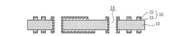
以下、図1〜図5を参照して、従来の技術に係る半導体パッケージ基板の製造方法を説明する。
まず、図1に示すように、絶縁層12の両面に銅箔層13が積層された両面銅張積層板11を準備する。次に、図2に示すように、ビアホール14および銅メッキ層15を形成した後、所定のパターンに応じてパターニングして両面に回路層16を形成する。
図3に示すように、接続パッドが露出されるように開口部を有する半田レジスト17を形成し、前記露出された接続パッドにニッケル/金メッキなどによる表面処理層18を形成する。
その後、図4に示すように、接続パッドの上部に半田ボール19を形成する。最後に、図5に示すように、半導体チップ20を半田ボール19の上部に位置させた後、リフロー装置30内に入れて加熱することにより、半導体チップ20の接続端子とベース基板10の接続パッドとを接合する。
リフロー工程は、半導体チップ20とベース基板10全体をリフロー装置30内に入れて半田ボール19の溶融温度以上に20〜30分間加熱する過程を経る。この際、ベース基板10全体を加熱するので、基板、半田ボール19および半導体チップ20間の熱膨張係数の差による大きい熱応力が存在する。また、ベース基板10に高温の熱を加えてからさらに冷却する場合、ベース基板10の膨張と収縮により上下の非対称性が発生してベース基板10が変形し、これにより半導体チップ20が接合位置から逸脱し、或いは半田ボール19の厚さが均一でなくて接合信頼性が低下するという問題が発生した。
そこで、本発明は、かかる問題点を解決するために創案されたもので、その目的は、半田層に電流印加配線の備えられた導電性発熱体を位置させ、前記電流印加配線に電流を流して半田層のみを局所的に加熱して半導体チップをベース基板の接続部に実装することにより、熱応力を減少させ、且つ半導体チップとベース基板間の接合信頼性を向上させることができる半導体パッケージ基板の製造方法を提供することにある。
上記目的を達成するために、本発明によれば、(A)上部に半田層が形成された接続部を一面に備えたベース基板を準備する段階と、(B)前記半田層の上部に、電流印加配線の備えられた導電性発熱体を配置する段階と、(C)前記電流印加配線に電流を印加して前記半田層を加熱することにより、半導体チップを前記接続部と接合する段階と、(D)前記導電性発熱体の前記電流印加配線を除去する段階とを含んでなる半導体パッケージ基板の製造方法を提供する。
ここで、本発明は、前記(C)段階の前に、前記導電性発熱体をカバーする補助半田層を積層する段階をさらに含むことを特徴とする。
また、本発明は、前記(C)段階で、前記ベース基板の他面を冷却する過程をさらに含むことを特徴とする。
また、本発明は、前記ベース基板の他面の温度を常温に維持しながら冷却することを特徴とする。
また、本発明は、前記(A)段階で、前記ベース基板は前記接続部の周辺に複数のリード部をさらに含み、前記(C)段階で、前記半導体チップは上部に複数のボンディングパッドをさらに含み、前記(C)段階の後、(E)複数の前記ボンディングパッドと複数の前記リード部をそれぞれ対応するように金属ワイヤーで接合する段階をさらに含むことを特徴とする。
また、本発明は、前記(A)段階で、前記ベース基板には複数の接続部を備え、前記(B)段階で、複数の前記接続部にそれぞれ対応するように、電流印加配線で接続された複数の導電性発熱体を配置し、前記(C)段階で、複数の半導体チップを前記複数の前記接続部と接合することを特徴とする。
また、本発明は、前記接続部が前記半田層に電気的に接続される少なくとも一つの接続パッドを含み、前記半導体チップが前記半田層に電気的に接続される少なくとも1つの接続端子を含むことを特徴とする。
また、本発明は、前記導電性発熱体がカーボンシートであることを特徴とする。
また、本発明は、前記導電性発熱体の大きさが前記半田層の大きさに対応することを特徴とする。
また、本発明は、前記導電性発熱体がメッシュ構造であることを特徴とする。
本発明に係る半導体パッケージ基板の製造方法は、ベース基板の接続部の上部に形成された半田層に電流印加配線の備えられた導電性発熱体を位置させ、前記電流印加配線に電流を流して加熱することにより、半導体チップを接続部に接合する。これにより、ベース基板の半田層のみを局所的に加熱するので、熱応力の減少および基板の変形を防止して半導体チップとベース基板間の接合信頼性を向上させることができる。
また、本発明によれば、ベース基板の他面を冷却することにより、半導体チップとベース基板の接続部のみを除いては、熱が伝達されないようにして接合信頼性を向上させる。
また、本発明によれば、ベース基板の接続部は半田層に電気的に接続される少なくとも一つの接続パッドを含み、半導体チップは半田層に電気的に接続される少なくとも一つの接続端子を含むため、ベース基板の接続部と半導体チップとを接合することにより半導体チップとベース基板内の回路層とを電気的に接続することができる。
また、本発明によれば、導電性発熱体は、カーボンシートで構成されるが、カーボンシートは、熱伝導性に優れるため、短時間で半田層を溶融温度以上に加熱することができ、半導体チップとベース基板の接続部とを接合するときに、半田層の内部に含浸されて半田層の機械的物性を向上させることができる。
本発明の目的、特定の利点および新規の特徴は、添付図面に連関する以下の詳細な説明と好適な実施例からさらに明白になるであろう。
これに先立ち、本明細書および請求の範囲に使用された用語または単語は、通常的で辞典的な意味で解釈されてはならず、発明者が自分の発明を最善の方法で説明するために用語の概念を適切に定義することができるという原則に基づき、本発明の技術的思想に符合する意味と概念で解釈されなければならない。
本発明において、各図面の構成要素に参照番号を付加するにおいて、同一の構成要素については、他の図面上に表示されても、出来る限り同一の番号を付することに留意すべきであろう。なお、本発明を説明するにおいて、関連した公知の技術に対する具体的な説明が本発明の要旨を無駄に乱すおそれがあると判断される場合、その詳細な説明は省略する。
以下、添付図面を参照して、本発明の好適な実施形態を詳細に説明する。
図6〜図12は、本発明の好適な実施例に係る半導体パッケージ基板の製造工程を順次示す図である。
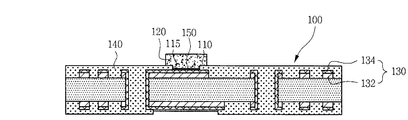
まず、図6に示すように、上部に半田層120が形成された接続部110を一面に備えたベース基板100を準備する。具体的に、前記ベース100を準備する段階は、接続部110を含み且つ内部に回路層130が形成されたベース基板100を準備する段階と、前記ベース基板100に半田レジスト140を形成する段階と、前記半田レジスト140に開口部を形成して接続部110の接続パッド115を露出させる段階と、半田層120を形成する段階とを含むことができる。
ベース基板100は、絶縁層に接続部110を含む少なくとも一つの回路が形成された回路基板であって、好ましくはプリント基板である。プリント基板(Printed Circuit Board、PCB)は、フェノール樹脂絶縁板またはエポキシ樹脂絶縁板などの絶縁材に形成された内層回路を介して実装された部品を電気的に相互接続し、電源などを供給すると同時に部品を機械的に固定させる役割を果たす。このようなプリント基板には、絶縁材の一面にのみ回路層130を形成した単面PCB、両面に回路層130を形成した両面PCB、および多層に配線したMLB(多層プリント基板)などがある。図6では、1つの絶縁層と2つの回路層130から構成される多層プリント基板を示したが、本発明は、これに限定されず、2つ以上の回路層130を持つ多層プリント基板が適用可能である。
接続部110は、後続工程によって上部に半田層120が形成され、前記半田層120を介して半導体チップ200または外部部品をベース基板100に実装する。
この際、接続部110は、少なくとも一つの接続パッド115を含むことができる。接続パッド115は、半田層120を介してベース基板100に実装される半導体チップ200と回路層130とを電気的に接続させる。接続パッド115は、銅、金、銀、ニッケルなどの伝導性金属で構成される。伝導性金属としては、一般に、銅が使用される。
半田レジスト140は、最外層回路を保護する機能を行い、接続部110の接続パッド115を露出させるために開口部が設けられる。半田レジスト140は、絶縁物質であって、半田レジストインク、半田レジストフィルムまたはカプセル化剤などで構成できるが、特にこれに限定されるのではない。
半田レジスト140の開口部を介して露出された接続部110の接続パッド115にさらに表面処理層150を形成することもできる。表面処理層150は、電解金メッキ(Electro Gold Plating)、無電解金メッキ(Immersion Gold Plating)、無電解銀メッキ(Immersion Silver Plating)、ENIG(Electroless Nickel and Immersion Gold、無電解ニッケルメッキ/置換金メッキ)、DIG(Direct Immersion Plating)、HASL(Hot Air Solder Levelling)などによって形成できる。
半田層120は、半導体チップ200などの外部部品とベース基板100の接続部110とを接合する機能を行い、スキージー(Squeegee)などのスクリーンプリント装置を用いて、露出された接続部110の上部に半田ペーストをプリントすることにより形成する。半田層120は、錫/鉛(Sn/Pb)、錫/銀/銅(Sn/Ag/Cu)、錫/銀(Sn/Ag)、錫/銅(Sn/Cu)、錫/ビスマス(Sn/Bi)、錫/亜鉛/ビスマス(Sn/Zn/Bi)、錫/銀/ビスマス(Sn/Ag/Bi)などの組み合わせで構成できる。
図7に示すように、半田層120の上部に、電流印加配線310の備えられた導電性発熱体300を配置する。導電性発熱体300の両端には、電流印加配線310が備えられ、電流印加配線310に電流を印加して半田層120を加熱する。このような導電性発熱体300は、電流が流れうる導体であって、銀、銅、ニクロムなどの金属であってもよい。半田層120が溶融点温度以上に加熱される場合、半導体チップ200とベース基板100の接続部110とが半田層120を介して接合されると同時に、前記導電性発熱体300が半田層120の内部に含浸される。
ここで、図8に示すように、導電性発熱体300をカバーする補助半田層160をさらに積層してもよい。補助半田層160を積層して導電性発熱体300を半田層120の内部に含浸させることにより、導電性発熱体300が含浸された状態で加熱を行い、半田層120を溶融点以上の温度にさらに速く加熱することができる。補助半田層160は、スキージーなどの方法で積層する。
この際、導電性発熱体300は、好ましくはカーボンシートである。カーボンシートは、炭素ナノチューブ(CNT)やグラフェン(Graphene)などの炭素ナノ物質と膨張黒鉛との混合物で構成される。カーボンシートは、電気伝導度および熱伝導率に優れるため、短時間で半田層120を効果的に加熱することを可能にすることにより、工程時間を短縮させる。
また、カーボンシートの場合、強度と弾性に優れるため、半田層120内にカーボンシートが含浸されることにより、半田層120の機械的物性を向上させる。カーボンシートは、熱膨張係数が小さいので、半田層120に含浸されて半田層120の熱膨張係数を低減させてベース基板100、半田層120および半導体チップ間の熱膨張係数の差を減少させる。
導電性発熱体300の大きさは、半田層120の大きさに対応することが好ましい。半田層120の大きさより導電性発熱体300の大きさが小さい場合、半田層120を溶融点以上に加熱するために多くの電力が消耗されるうえ、加熱時間が長くなるという欠点がある。これに対し、半田層120の大きさより導電性発熱体300の大きさが大きい場合、半田層120のみを局所的に加熱することが難しいという問題点がある。
また、図9に示すように、導電性発熱体300は、メッシュ構造であることが好ましく、メッシュ構造で形成された場合、半田層120の全面に均一に熱を伝達して半田層を効果的に加熱することができる。また、半田層120の内部に導電性発熱体300が単位面積当たり均一に含浸されることにより、半田層120の機械的物性を向上させる効果を高めることができる。
図10に示すように、導電性発熱体300の電流印加配線310に電流を印加して半田層120を加熱することにより、半導体チップ200をベース基板100の接続部110と接合する。導電性発熱体300に電流が流れるときに抵抗により熱が発生するが、これを用いて半田層120を溶融温度以上に加熱する。電流印加配線310に流れる電流量を調節して精密に加熱温度を制御することができるという利点がある。導電性発熱体300の電流印加配線310に電流を流して半田層120のみを局所的に加熱することにより、基板の変形を防止し、且つ熱膨張係数の差による熱応力を減少させることができる。
ベース基板100に接合される半導体チップ200は、少なくとも一つの接続端子を含み、ベース基板100の接続部110は、少なくとも一つの接続パッド115を含むので、半導体チップ200とベース基板100の接続部110とが半田層120を介して接合されることにより、ベース基板100の回路層130と半導体チップ200とが電気的に接続され得る。
この際、図11に示すように、半田層120を加熱して半導体チップ200を接合するとき、ベース基板100の他面を冷却する過程をさらに含んでもよい。一面に半導体チップ200が接合されるベース基板100の他面を冷却装置400によって冷却することにより、導電性発熱体300により発生する熱が半田層120以外のベース基板100の他の領域に及ばないようにして、熱によるベース基板100の変形をさらに徹底的に防止することができる。
ベース基板100の他面を常温に維持しながら冷却することが好ましい。これは、ベース基板100および他の実装部品の温度による影響が常温で最も少ないためである。
次に、図12に示すように、前記導電性発熱体300の電流印加配線310を除去する。
本発明に係る製造方法は、前述した方式の半導体チップ200の接合に限定されず、ワイヤー220を用いた半導体チップ200の接合にも適用できる。ワイヤー220を用いた半導体チップ200の接合の場合、図13に示すように、ベース基板100は、接続部110の周辺部に複数のリード部170をさらに含む。前記リード部170は、ベース基板100の回路層130に電気的に接続される。
半田層120の上部に電流印加配線310の備えられた導電性発熱体300を位置させ、電流を印加して半田層120を加熱することにより、半導体チップ200を接続部110に接合する。
ワイヤー220を用いた半導体チップ200の接合の場合、半導体チップ200の上部に複数のボンディングパッド210を備えて、半導体チップ200上部の複数のボンディングパッド210とベース基板100の複数のリード部170とをそれぞれ対応するようにワイヤー220で接合する工程をさらに含む。ワイヤー220としては、一般に、金(Au)またはアルミニウム(Al)を使用する。この際、リード部170に接続されたワイヤー220を介してのみ半導体チップ200とベース基板100の回路層130とが電気的に接続されるのではなく、接続部110に形成された接続パッド115を介しても半導体チップ200とベース基板100の回路層130とが電気的に接続できる。
その次、導電性発熱体300に接続された電流印加配線310を除去する。前記電流印加配線310を除去する工程は、ベース基板100とリード部170とをワイヤー220で接合する前に行ってもよい。
また、図14および図15に示すように、複数の半導体チップ200をベース基板100に一度に接合することができる。図14に示すように、ベース基板100には、複数の接続部110を備え、複数の前記接続部110にそれぞれ対応するように、電流印加配線310で接続された複数の導電性発熱体300を半田層120の上部に配置する。
導電性発熱体300の電流印加配線310の両端に電流を印加して複数の半導体チップ200をベース基板100の接続部110に接合し、図15に示すように、複数の導電性発熱体300に接続された電流印加配線310を除去する。前述したように既存のリフロー工程と同様に、本発明によっても複数の半導体チップ200をベース基板100の接続部110に一度に接合することができる。
以上、本発明を具体的な実施例に基づいて詳細に説明したが、これは、本発明を具体的に説明するためのものに過ぎず、本発明による半導体パッケージ基板の製造方法は、これに限定されず、当該分野における通常の知識を有する者であれば、 本発明の技術的思想の範疇内で多様な変形および改良を加え得るのは明白であろう。それらの単純な変形ないし変更は、いずれも本発明の範疇内に属するものであり、本発明の具体的な保護範囲は、特許請求の範囲によって明確に定められるであろう。
本発明は、熱応力を減少させ、且つ半導体チップとベース基板間の接合信頼性を向上させることができる半導体パッケージ基板の製造方法に適用可能である。
10、100 ベース基板
11 両面銅張積層板
12 絶縁層
13、132 銅箔層
14 ビアホール
15、134 メッキ層
16、130 回路層
17、140 半田レジスト
18、150 表面処理層
19 半田ボール
20、200 半導体チップ
30 リフロー装置
110 接続部
115 接続パッド
120 半田層
160 補助半田層
170 リード部
210 ボンディングパッド
220 ワイヤー
300 導電性発熱体
310 電流印加配線
400 冷却装置
11 両面銅張積層板
12 絶縁層
13、132 銅箔層
14 ビアホール
15、134 メッキ層
16、130 回路層
17、140 半田レジスト
18、150 表面処理層
19 半田ボール
20、200 半導体チップ
30 リフロー装置
110 接続部
115 接続パッド
120 半田層
160 補助半田層
170 リード部
210 ボンディングパッド
220 ワイヤー
300 導電性発熱体
310 電流印加配線
400 冷却装置
Claims (10)
- (A)上部に半田層が形成された接続部を一面に備えたベース基板を準備する段階と、
(B)前記半田層の上部に、電流印加配線の備えられた導電性発熱体を配置する段階と、
(C)前記電流印加配線に電流を印加して前記半田層を加熱することにより、半導体チップを前記接続部と接合する段階と、
(D)前記導電性発熱体の前記電流印加配線を除去する段階とを含んでなることを特徴とする半導体パッケージ基板の製造方法。 - 前記(C)段階の前に、
前記導電性発熱体をカバーする補助半田層を積層する段階をさらに含むことを特徴とする請求項1に記載の半導体パッケージ基板の製造方法。 - 前記(C)段階で、前記ベース基板の他面を冷却する過程をさらに含むことを特徴とする請求項1に記載の半導体パッケージ基板の製造方法。
- 前記ベース基板の他面の温度を常温に維持しながら冷却することを特徴とする請求項3に記載の半導体パッケージ基板の製造方法。
- 前記(A)段階で、前記ベース基板は前記接続部の周辺に複数のリード部をさらに含み、
前記(C)段階で、前記半導体チップは上部に複数のボンディングパッドをさらに含み、
前記(C)段階の後、(E)複数の前記ボンディングパッドと複数の前記リード部をそれぞれ対応するように金属ワイヤーで接合する段階をさらに含むことを特徴とする請求項1に記載の半導体パッケージ基板の製造方法。 - 前記(A)段階で、前記ベース基板には複数の接続部を備え、
前記(B)段階で、複数の前記接続部にそれぞれ対応するように、電流印加配線で接続された複数の導電性発熱体を配置し、
前記(C)段階で、複数の半導体チップを前記複数の前記接続部と接合することを特徴とする請求項1に記載の半導体パッケージ基板の製造方法。 - 前記接続部は前記半田層に電気的に接続される少なくとも一つの接続パッドを含み、前記半導体チップは前記半田層に電気的に接続される少なくとも1つの接続端子を含むことを特徴とする請求項1に記載の半導体パッケージ基板の製造方法。
- 前記導電性発熱体がカーボンシートであることを特徴とする請求項1に記載の半導体パッケージ基板の製造方法。
- 前記導電性発熱体の大きさが前記半田層の大きさに対応することを特徴とする請求項1に記載の半導体パッケージ基板の製造方法。
- 前記導電性発熱体がメッシュ構造であることを特徴とする請求項1に記載の半導体パッケージ基板の製造方法。
Applications Claiming Priority (2)
| Application Number | Priority Date | Filing Date | Title |
|---|---|---|---|
| KR10-2010-0112281 | 2010-11-11 | ||
| KR1020100112281A KR20120050834A (ko) | 2010-11-11 | 2010-11-11 | 반도체 패키지 기판의 제조방법 |
Publications (1)
| Publication Number | Publication Date |
|---|---|
| JP2012104792A true JP2012104792A (ja) | 2012-05-31 |
Family
ID=46048149
Family Applications (1)
| Application Number | Title | Priority Date | Filing Date |
|---|---|---|---|
| JP2011003258A Pending JP2012104792A (ja) | 2010-11-11 | 2011-01-11 | 半導体パッケージ基板の製造方法 |
Country Status (4)
| Country | Link |
|---|---|
| US (1) | US20120122278A1 (ja) |
| JP (1) | JP2012104792A (ja) |
| KR (1) | KR20120050834A (ja) |
| CN (1) | CN102469698A (ja) |
Families Citing this family (4)
| Publication number | Priority date | Publication date | Assignee | Title |
|---|---|---|---|---|
| KR102055361B1 (ko) | 2013-06-05 | 2019-12-12 | 삼성전자주식회사 | 반도체 패키지 |
| TWI613775B (zh) | 2016-08-24 | 2018-02-01 | 國立清華大學 | 降低電流路徑熱應力之晶片 |
| US11051407B2 (en) * | 2018-10-23 | 2021-06-29 | International Business Machines Corporation | Facilitating filling a plated through-hole of a circuit board with solder |
| CN116564906A (zh) * | 2022-01-28 | 2023-08-08 | 群创光电股份有限公司 | 电子装置 |
Citations (4)
| Publication number | Priority date | Publication date | Assignee | Title |
|---|---|---|---|---|
| JPH09213740A (ja) * | 1996-01-29 | 1997-08-15 | Citizen Watch Co Ltd | 液晶表示装置における液晶駆動用半導体装置の実装方法 |
| JP2000260827A (ja) * | 1999-03-12 | 2000-09-22 | Towa Corp | 半導体チップ実装用加熱装置及び加熱方法 |
| JP2003124624A (ja) * | 2001-10-18 | 2003-04-25 | Canon Inc | ヒートコネクタ |
| JP2010129967A (ja) * | 2008-12-01 | 2010-06-10 | Alps Electric Co Ltd | 電子回路モジュール |
Family Cites Families (6)
| Publication number | Priority date | Publication date | Assignee | Title |
|---|---|---|---|---|
| US6984571B1 (en) * | 1999-10-01 | 2006-01-10 | Ziptronix, Inc. | Three dimensional device integration method and integrated device |
| JP3649169B2 (ja) * | 2001-08-08 | 2005-05-18 | 松下電器産業株式会社 | 半導体装置 |
| US6919224B2 (en) * | 2003-09-30 | 2005-07-19 | Intel Corporation | Modified chip attach process and apparatus |
| US7364063B2 (en) * | 2004-08-09 | 2008-04-29 | Intel Corporation | Thermally coupling an integrated heat spreader to a heat sink base |
| US20070034676A1 (en) * | 2005-08-11 | 2007-02-15 | Honeywell International Inc. | Electric field assisted solder bonding |
| US8034662B2 (en) * | 2009-03-18 | 2011-10-11 | Advanced Micro Devices, Inc. | Thermal interface material with support structure |
-
2010
- 2010-11-11 KR KR1020100112281A patent/KR20120050834A/ko not_active Withdrawn
-
2011
- 2011-01-11 JP JP2011003258A patent/JP2012104792A/ja active Pending
- 2011-01-14 CN CN2011100240783A patent/CN102469698A/zh active Pending
- 2011-01-14 US US13/007,530 patent/US20120122278A1/en not_active Abandoned
Patent Citations (4)
| Publication number | Priority date | Publication date | Assignee | Title |
|---|---|---|---|---|
| JPH09213740A (ja) * | 1996-01-29 | 1997-08-15 | Citizen Watch Co Ltd | 液晶表示装置における液晶駆動用半導体装置の実装方法 |
| JP2000260827A (ja) * | 1999-03-12 | 2000-09-22 | Towa Corp | 半導体チップ実装用加熱装置及び加熱方法 |
| JP2003124624A (ja) * | 2001-10-18 | 2003-04-25 | Canon Inc | ヒートコネクタ |
| JP2010129967A (ja) * | 2008-12-01 | 2010-06-10 | Alps Electric Co Ltd | 電子回路モジュール |
Also Published As
| Publication number | Publication date |
|---|---|
| US20120122278A1 (en) | 2012-05-17 |
| CN102469698A (zh) | 2012-05-23 |
| KR20120050834A (ko) | 2012-05-21 |
Similar Documents
| Publication | Publication Date | Title |
|---|---|---|
| JP4159861B2 (ja) | プリント回路基板の放熱構造の製造方法 | |
| JP5122932B2 (ja) | 多層配線基板 | |
| JP3619395B2 (ja) | 半導体素子内蔵配線基板およびその製造方法 | |
| JP4669392B2 (ja) | メタルコア多層プリント配線板 | |
| WO1998040914A1 (fr) | Carte imprimee et son procede de fabrication | |
| WO2007126090A1 (ja) | 回路基板、電子デバイス装置及び回路基板の製造方法 | |
| JP2010010640A (ja) | 電子部品組込み型印刷回路基板及びその製造方法 | |
| WO2002087296A1 (en) | Circuit board, circuit board mounting method, and electronic device using the circuit board | |
| JPWO2009104506A1 (ja) | プリント配線板、電子装置及びその製造方法 | |
| JP2010199216A (ja) | 部品実装構造及び部品実装方法 | |
| CN111148353B (zh) | 具有铜基散热体的电路板的制备方法 | |
| JPWO2010103695A1 (ja) | 部品内蔵モジュールの製造方法及び部品内蔵モジュール | |
| JP2001217550A (ja) | 多層回路基板および半導体装置 | |
| CN102077701B (zh) | 印刷电路板、印刷电路板的制造方法以及电子设备 | |
| TW201427523A (zh) | 晶片封裝結構、具有內埋元件的電路板及其製作方法 | |
| JP2012104792A (ja) | 半導体パッケージ基板の製造方法 | |
| CN101951725A (zh) | 印刷电路板单元和电子装置 | |
| JP2014179430A (ja) | 半導体素子搭載用多層プリント配線板 | |
| JP5397012B2 (ja) | 部品内蔵配線板、部品内蔵配線板の製造方法 | |
| JP2004055967A (ja) | 電子部品内蔵基板の製造方法 | |
| JP2833642B2 (ja) | 多層配線基板及びその製造方法 | |
| JP3862454B2 (ja) | 金属ベース多層回路基板 | |
| CN111093320A (zh) | 金属散热双面电路板的制备方法 | |
| JP3988629B2 (ja) | 電子装置 | |
| JP2004179171A (ja) | 配線基板 |
Legal Events
| Date | Code | Title | Description |
|---|---|---|---|
| A977 | Report on retrieval |
Free format text: JAPANESE INTERMEDIATE CODE: A971007 Effective date: 20130214 |
|
| A131 | Notification of reasons for refusal |
Free format text: JAPANESE INTERMEDIATE CODE: A131 Effective date: 20130305 |
|
| A02 | Decision of refusal |
Free format text: JAPANESE INTERMEDIATE CODE: A02 Effective date: 20130903 |