JP2012104532A - 測定方法および測定装置 - Google Patents
測定方法および測定装置 Download PDFInfo
- Publication number
- JP2012104532A JP2012104532A JP2010249430A JP2010249430A JP2012104532A JP 2012104532 A JP2012104532 A JP 2012104532A JP 2010249430 A JP2010249430 A JP 2010249430A JP 2010249430 A JP2010249430 A JP 2010249430A JP 2012104532 A JP2012104532 A JP 2012104532A
- Authority
- JP
- Japan
- Prior art keywords
- protective film
- light
- thickness
- measuring
- wavelength
- Prior art date
- Legal status (The legal status is an assumption and is not a legal conclusion. Google has not performed a legal analysis and makes no representation as to the accuracy of the status listed.)
- Granted
Links
- 238000000034 method Methods 0.000 title claims abstract description 50
- 230000001681 protective effect Effects 0.000 claims abstract description 210
- 238000005259 measurement Methods 0.000 claims abstract description 82
- 238000001228 spectrum Methods 0.000 claims abstract description 55
- 230000003287 optical effect Effects 0.000 claims abstract description 46
- 230000008859 change Effects 0.000 claims abstract description 22
- 238000010521 absorption reaction Methods 0.000 claims abstract description 6
- 238000012545 processing Methods 0.000 claims description 97
- 230000002745 absorbent Effects 0.000 claims description 37
- 239000002250 absorbent Substances 0.000 claims description 37
- 230000008569 process Effects 0.000 claims description 31
- 239000011347 resin Substances 0.000 claims description 22
- 229920005989 resin Polymers 0.000 claims description 22
- 238000003860 storage Methods 0.000 claims description 12
- 238000000691 measurement method Methods 0.000 claims description 8
- 239000006096 absorbing agent Substances 0.000 claims description 5
- 239000002699 waste material Substances 0.000 claims description 4
- 230000001678 irradiating effect Effects 0.000 abstract description 6
- 230000031700 light absorption Effects 0.000 abstract 1
- 235000012431 wafers Nutrition 0.000 description 94
- 230000007246 mechanism Effects 0.000 description 36
- 230000015572 biosynthetic process Effects 0.000 description 14
- 238000005755 formation reaction Methods 0.000 description 14
- 239000004065 semiconductor Substances 0.000 description 14
- 238000003384 imaging method Methods 0.000 description 10
- 239000007788 liquid Substances 0.000 description 9
- 238000004140 cleaning Methods 0.000 description 8
- 238000012546 transfer Methods 0.000 description 6
- 238000010586 diagram Methods 0.000 description 5
- 238000009826 distribution Methods 0.000 description 5
- 230000007723 transport mechanism Effects 0.000 description 5
- 239000006097 ultraviolet radiation absorber Substances 0.000 description 5
- 230000006866 deterioration Effects 0.000 description 4
- 230000006870 function Effects 0.000 description 3
- 238000003672 processing method Methods 0.000 description 3
- XLYOFNOQVPJJNP-UHFFFAOYSA-N water Substances O XLYOFNOQVPJJNP-UHFFFAOYSA-N 0.000 description 3
- GYHNNYVSQQEPJS-UHFFFAOYSA-N Gallium Chemical compound [Ga] GYHNNYVSQQEPJS-UHFFFAOYSA-N 0.000 description 2
- 239000004372 Polyvinyl alcohol Substances 0.000 description 2
- 150000001875 compounds Chemical class 0.000 description 2
- 230000008602 contraction Effects 0.000 description 2
- 229910052733 gallium Inorganic materials 0.000 description 2
- 239000000463 material Substances 0.000 description 2
- 230000004048 modification Effects 0.000 description 2
- 238000012986 modification Methods 0.000 description 2
- 229920002451 polyvinyl alcohol Polymers 0.000 description 2
- 238000002360 preparation method Methods 0.000 description 2
- JYEUMXHLPRZUAT-UHFFFAOYSA-N 1,2,3-triazine Chemical compound C1=CN=NN=C1 JYEUMXHLPRZUAT-UHFFFAOYSA-N 0.000 description 1
- 229910001218 Gallium arsenide Inorganic materials 0.000 description 1
- XUIMIQQOPSSXEZ-UHFFFAOYSA-N Silicon Chemical compound [Si] XUIMIQQOPSSXEZ-UHFFFAOYSA-N 0.000 description 1
- 230000005856 abnormality Effects 0.000 description 1
- 239000000853 adhesive Substances 0.000 description 1
- 230000001070 adhesive effect Effects 0.000 description 1
- WPYMKLBDIGXBTP-UHFFFAOYSA-N benzoic acid Chemical compound OC(=O)C1=CC=CC=C1 WPYMKLBDIGXBTP-UHFFFAOYSA-N 0.000 description 1
- RWCCWEUUXYIKHB-UHFFFAOYSA-N benzophenone Chemical compound C=1C=CC=CC=1C(=O)C1=CC=CC=C1 RWCCWEUUXYIKHB-UHFFFAOYSA-N 0.000 description 1
- 239000012965 benzophenone Substances 0.000 description 1
- QRUDEWIWKLJBPS-UHFFFAOYSA-N benzotriazole Chemical compound C1=CC=C2N[N][N]C2=C1 QRUDEWIWKLJBPS-UHFFFAOYSA-N 0.000 description 1
- 239000012964 benzotriazole Substances 0.000 description 1
- 230000015556 catabolic process Effects 0.000 description 1
- 239000000919 ceramic Substances 0.000 description 1
- 229910010293 ceramic material Inorganic materials 0.000 description 1
- 239000012141 concentrate Substances 0.000 description 1
- 238000006731 degradation reaction Methods 0.000 description 1
- 230000000694 effects Effects 0.000 description 1
- 239000011521 glass Substances 0.000 description 1
- 229910010272 inorganic material Inorganic materials 0.000 description 1
- 239000011147 inorganic material Substances 0.000 description 1
- 239000004973 liquid crystal related substance Substances 0.000 description 1
- 238000003754 machining Methods 0.000 description 1
- TWNQGVIAIRXVLR-UHFFFAOYSA-N oxo(oxoalumanyloxy)alumane Chemical compound O=[Al]O[Al]=O TWNQGVIAIRXVLR-UHFFFAOYSA-N 0.000 description 1
- 239000004597 plastic additive Substances 0.000 description 1
- 229910052710 silicon Inorganic materials 0.000 description 1
- 239000010703 silicon Substances 0.000 description 1
- HBMJWWWQQXIZIP-UHFFFAOYSA-N silicon carbide Chemical compound [Si+]#[C-] HBMJWWWQQXIZIP-UHFFFAOYSA-N 0.000 description 1
- 230000003595 spectral effect Effects 0.000 description 1
- 239000007921 spray Substances 0.000 description 1
- 238000005507 spraying Methods 0.000 description 1
- 239000000758 substrate Substances 0.000 description 1
- 238000005979 thermal decomposition reaction Methods 0.000 description 1
Images


Classifications
-
- G—PHYSICS
- G01—MEASURING; TESTING
- G01B—MEASURING LENGTH, THICKNESS OR SIMILAR LINEAR DIMENSIONS; MEASURING ANGLES; MEASURING AREAS; MEASURING IRREGULARITIES OF SURFACES OR CONTOURS
- G01B11/00—Measuring arrangements characterised by the use of optical techniques
- G01B11/02—Measuring arrangements characterised by the use of optical techniques for measuring length, width or thickness
- G01B11/06—Measuring arrangements characterised by the use of optical techniques for measuring length, width or thickness for measuring thickness ; e.g. of sheet material
- G01B11/0616—Measuring arrangements characterised by the use of optical techniques for measuring length, width or thickness for measuring thickness ; e.g. of sheet material of coating
- G01B11/0625—Measuring arrangements characterised by the use of optical techniques for measuring length, width or thickness for measuring thickness ; e.g. of sheet material of coating with measurement of absorption or reflection
-
- G—PHYSICS
- G01—MEASURING; TESTING
- G01B—MEASURING LENGTH, THICKNESS OR SIMILAR LINEAR DIMENSIONS; MEASURING ANGLES; MEASURING AREAS; MEASURING IRREGULARITIES OF SURFACES OR CONTOURS
- G01B9/00—Measuring instruments characterised by the use of optical techniques
- G01B9/02—Interferometers
- G01B9/0209—Low-coherence interferometers
-
- G—PHYSICS
- G01—MEASURING; TESTING
- G01N—INVESTIGATING OR ANALYSING MATERIALS BY DETERMINING THEIR CHEMICAL OR PHYSICAL PROPERTIES
- G01N21/00—Investigating or analysing materials by the use of optical means, i.e. using sub-millimetre waves, infrared, visible or ultraviolet light
- G01N21/17—Systems in which incident light is modified in accordance with the properties of the material investigated
- G01N21/55—Specular reflectivity
-
- G—PHYSICS
- G01—MEASURING; TESTING
- G01N—INVESTIGATING OR ANALYSING MATERIALS BY DETERMINING THEIR CHEMICAL OR PHYSICAL PROPERTIES
- G01N21/00—Investigating or analysing materials by the use of optical means, i.e. using sub-millimetre waves, infrared, visible or ultraviolet light
- G01N21/84—Systems specially adapted for particular applications
- G01N21/8483—Investigating reagent band
-
- G—PHYSICS
- G01—MEASURING; TESTING
- G01N—INVESTIGATING OR ANALYSING MATERIALS BY DETERMINING THEIR CHEMICAL OR PHYSICAL PROPERTIES
- G01N21/00—Investigating or analysing materials by the use of optical means, i.e. using sub-millimetre waves, infrared, visible or ultraviolet light
- G01N21/84—Systems specially adapted for particular applications
- G01N21/88—Investigating the presence of flaws or contamination
- G01N21/95—Investigating the presence of flaws or contamination characterised by the material or shape of the object to be examined
- G01N21/9501—Semiconductor wafers
-
- H—ELECTRICITY
- H01—ELECTRIC ELEMENTS
- H01L—SEMICONDUCTOR DEVICES NOT COVERED BY CLASS H10
- H01L22/00—Testing or measuring during manufacture or treatment; Reliability measurements, i.e. testing of parts without further processing to modify the parts as such; Structural arrangements therefor
Landscapes
- General Physics & Mathematics (AREA)
- Physics & Mathematics (AREA)
- Health & Medical Sciences (AREA)
- Life Sciences & Earth Sciences (AREA)
- Chemical & Material Sciences (AREA)
- Analytical Chemistry (AREA)
- Biochemistry (AREA)
- General Health & Medical Sciences (AREA)
- Immunology (AREA)
- Pathology (AREA)
- Engineering & Computer Science (AREA)
- Molecular Biology (AREA)
- Manufacturing & Machinery (AREA)
- Computer Hardware Design (AREA)
- Microelectronics & Electronic Packaging (AREA)
- Power Engineering (AREA)
- Laser Beam Processing (AREA)
- Dicing (AREA)
- Testing Or Measuring Of Semiconductors Or The Like (AREA)
- Length Measuring Devices By Optical Means (AREA)
Abstract
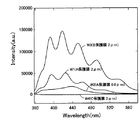
【解決手段】本発明の測定方法は、ウェーハWに光吸収剤を含む保護膜61を形成するステップと、保護膜61に測定光を照射し、測定光の吸収による保護膜61の発光を受光するステップと、事前に作製された保護膜61の厚みの変化に対する保護膜61の発光による光スペクトルの変化を示す測定データを参照して、保護膜61の発光強度から保護膜61の厚みを測定するステップとを有する構成とした。
【選択図】図5
Description
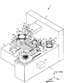
11 搬入搬出機構
12 保護膜形成機構
13 チャックテーブル
14 レーザー加工ユニット
15 厚み測定ユニット
16 プッシュプル機構
18 搬送機構
19 制御部(記憶手段、算出手段)
28 液状樹脂供給部
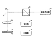
52 測定ヘッド
53 加工ヘッド
54 撮像ヘッド
55 測定用光源(光照射部)
56 ハーフミラー(光照射部)
57 ミラー(光照射部)
58、66 集光レンズ(光照射部)
59 受光部
61 保護膜
65 白色光源(光照射部)
W ウェーハ(ワーク)
Claims (3)
- ワークをレーザー加工する際に発生する加工屑からワークの表面を保護するために前記レーザーの波長の光を吸収する吸収剤を含んだ水溶性樹脂によって形成された保護膜の厚みを測定する測定方法であって、
前記吸収材を含んだ水溶性樹脂によってワーク表面に所定の厚みとなる様に前記保護膜を形成する保護膜形成工程と、
前記保護膜形成工程の後に、ワーク表面に形成された前記保護膜に前記吸収剤が吸収する波長の光を照射して、該光の吸収によって前記吸収剤が発光する光スペクトルを受光して測定するスペクトル測定工程と、
前記保護膜形成工程で形成する前記保護膜の厚みを変化させながら前記スペクトル測定工程を行うことで前記保護膜の厚み変化に対する前記光スペクトルの変化を表すマップを作製するマップ作製工程を含み、
ワークの表面に塗布された前記保護膜の厚みを測定する際は、
前記保護膜に前記吸収剤が吸収する波長の光を照射して前記光スペクトルを測定し、前記マップに基づいて前記保護膜の厚みを測定する保護膜厚み測定工程を実施することを特徴とする測定方法。 - 前記吸収剤が吸収する光の波長は少なくとも250nm以上かつ380nm以下、もしくは460nm以上かつ650nm以下のいずれかの波長を含むことを特徴とする請求項1に記載の測定方法。
- ワークをレーザー加工する際に発生する加工屑からワークの表面を保護するために前記レーザーの波長の光を吸収する吸収剤を含んだ水溶性樹脂によって形成された保護膜の厚みを測定する測定装置であって、
前記吸収剤が吸収する波長の光をワーク表面に形成された保護膜に向けて照射する光照射部と、
前記吸収剤が前記光照射部からの光を吸収して発光する光スペクトルを受光する受光部と、
前記保護膜の厚み変化に対する前記光スペクトルの変化を表すマップを記憶する記憶手段と、
前記受光部で受光した光スペクトルと前記記憶手段で記憶した前記マップに基づいて前記保護膜の厚みを求める算出手段と、を有することを特徴とする測定装置。
Priority Applications (3)
| Application Number | Priority Date | Filing Date | Title |
|---|---|---|---|
| JP2010249430A JP5681452B2 (ja) | 2010-11-08 | 2010-11-08 | 測定方法および測定装置 |
| KR1020110111215A KR101835888B1 (ko) | 2010-11-08 | 2011-10-28 | 측정 방법 및 측정 장치 |
| CN2011103512173A CN102564328A (zh) | 2010-11-08 | 2011-11-08 | 测定方法以及测定装置 |
Applications Claiming Priority (1)
| Application Number | Priority Date | Filing Date | Title |
|---|---|---|---|
| JP2010249430A JP5681452B2 (ja) | 2010-11-08 | 2010-11-08 | 測定方法および測定装置 |
Publications (2)
| Publication Number | Publication Date |
|---|---|
| JP2012104532A true JP2012104532A (ja) | 2012-05-31 |
| JP5681452B2 JP5681452B2 (ja) | 2015-03-11 |
Family
ID=46267162
Family Applications (1)
| Application Number | Title | Priority Date | Filing Date |
|---|---|---|---|
| JP2010249430A Active JP5681452B2 (ja) | 2010-11-08 | 2010-11-08 | 測定方法および測定装置 |
Country Status (3)
| Country | Link |
|---|---|
| JP (1) | JP5681452B2 (ja) |
| KR (1) | KR101835888B1 (ja) |
| CN (1) | CN102564328A (ja) |
Cited By (6)
| Publication number | Priority date | Publication date | Assignee | Title |
|---|---|---|---|---|
| JP2017112296A (ja) * | 2015-12-18 | 2017-06-22 | 株式会社ディスコ | レーザー加工用保護膜検出方法 |
| JP2017120248A (ja) * | 2015-12-29 | 2017-07-06 | テスト リサーチ, インク. | 光学検出装置 |
| DE102017209946A1 (de) | 2016-06-22 | 2017-12-28 | Disco Corporation | Fluoreszenzdetektionsvorrichtung |
| KR20200110090A (ko) * | 2019-03-15 | 2020-09-23 | 한국세라믹기술원 | 결정 성장 방법에 의하여 제조된 탄화규소의 자외선을 이용한 두께 측정 장치 및 측정 방법 |
| JP2020533787A (ja) * | 2017-09-06 | 2020-11-19 | ラム リサーチ コーポレーションLam Research Corporation | 光計測を質量計測と組合せるためのシステム及び方法 |
| JP7387227B2 (ja) | 2019-10-07 | 2023-11-28 | 株式会社ディスコ | ウェーハの加工方法 |
Families Citing this family (2)
| Publication number | Priority date | Publication date | Assignee | Title |
|---|---|---|---|---|
| CN103433619B (zh) * | 2013-08-30 | 2015-10-21 | 大族激光科技产业集团股份有限公司 | 激光熔覆打印机及线路板的制作方法 |
| JP6478728B2 (ja) * | 2015-03-11 | 2019-03-06 | 株式会社ディスコ | 保護膜検出方法 |
Citations (5)
| Publication number | Priority date | Publication date | Assignee | Title |
|---|---|---|---|---|
| JPS6243503A (ja) * | 1985-08-20 | 1987-02-25 | Toyota Motor Corp | メタリツク塗装クリヤ−塗膜の膜厚測定法 |
| JP2006140311A (ja) * | 2004-11-12 | 2006-06-01 | Tokyo Ohka Kogyo Co Ltd | レーザーダイシング用保護膜剤及び該保護膜剤を用いたウエーハの加工方法 |
| JP2006162627A (ja) * | 2004-12-07 | 2006-06-22 | Samsung Electro Mech Co Ltd | 金属表面上の有機塗膜の厚さ測定方法 |
| JP2008229706A (ja) * | 2007-03-23 | 2008-10-02 | Disco Abrasive Syst Ltd | レーザー加工装置 |
| JP2009103630A (ja) * | 2007-10-25 | 2009-05-14 | Nippon Soken Inc | 液膜厚さ計測装置及び内燃機関の制御装置 |
Family Cites Families (6)
| Publication number | Priority date | Publication date | Assignee | Title |
|---|---|---|---|---|
| JP3624476B2 (ja) * | 1995-07-17 | 2005-03-02 | セイコーエプソン株式会社 | 半導体レーザ装置の製造方法 |
| JP3908472B2 (ja) | 2001-03-13 | 2007-04-25 | 株式会社東芝 | 膜厚測定方法及び段差測定方法 |
| CN1173166C (zh) * | 2002-08-22 | 2004-10-27 | 上海交通大学 | 双面金属波导测量方法及其装置 |
| JP2004322168A (ja) * | 2003-04-25 | 2004-11-18 | Disco Abrasive Syst Ltd | レーザー加工装置 |
| JP2010012508A (ja) * | 2008-07-07 | 2010-01-21 | Disco Abrasive Syst Ltd | 保護膜被覆装置及びレーザー加工装置 |
| CN104864818B (zh) * | 2008-07-24 | 2018-09-11 | 麻省理工学院 | 用于使用吸收来成像的系统和方法 |
-
2010
- 2010-11-08 JP JP2010249430A patent/JP5681452B2/ja active Active
-
2011
- 2011-10-28 KR KR1020110111215A patent/KR101835888B1/ko active Search and Examination
- 2011-11-08 CN CN2011103512173A patent/CN102564328A/zh active Pending
Patent Citations (5)
| Publication number | Priority date | Publication date | Assignee | Title |
|---|---|---|---|---|
| JPS6243503A (ja) * | 1985-08-20 | 1987-02-25 | Toyota Motor Corp | メタリツク塗装クリヤ−塗膜の膜厚測定法 |
| JP2006140311A (ja) * | 2004-11-12 | 2006-06-01 | Tokyo Ohka Kogyo Co Ltd | レーザーダイシング用保護膜剤及び該保護膜剤を用いたウエーハの加工方法 |
| JP2006162627A (ja) * | 2004-12-07 | 2006-06-22 | Samsung Electro Mech Co Ltd | 金属表面上の有機塗膜の厚さ測定方法 |
| JP2008229706A (ja) * | 2007-03-23 | 2008-10-02 | Disco Abrasive Syst Ltd | レーザー加工装置 |
| JP2009103630A (ja) * | 2007-10-25 | 2009-05-14 | Nippon Soken Inc | 液膜厚さ計測装置及び内燃機関の制御装置 |
Cited By (17)
| Publication number | Priority date | Publication date | Assignee | Title |
|---|---|---|---|---|
| KR20170073486A (ko) * | 2015-12-18 | 2017-06-28 | 가부시기가이샤 디스코 | 레이저 가공용 보호막 검출 방법 |
| KR102523679B1 (ko) * | 2015-12-18 | 2023-04-19 | 가부시기가이샤 디스코 | 레이저 가공용 보호막 검출 방법 |
| JP2017112296A (ja) * | 2015-12-18 | 2017-06-22 | 株式会社ディスコ | レーザー加工用保護膜検出方法 |
| TWI691375B (zh) * | 2015-12-18 | 2020-04-21 | 日商迪思科股份有限公司 | 雷射加工用保護膜檢測方法 |
| US10600174B2 (en) | 2015-12-29 | 2020-03-24 | Test Research, Inc. | Optical inspection apparatus |
| JP2017120248A (ja) * | 2015-12-29 | 2017-07-06 | テスト リサーチ, インク. | 光学検出装置 |
| JP2017227532A (ja) * | 2016-06-22 | 2017-12-28 | 株式会社ディスコ | 蛍光検出装置 |
| US9989468B2 (en) | 2016-06-22 | 2018-06-05 | Disco Corporation | Fluorescence detecting apparatus |
| KR20180000304A (ko) | 2016-06-22 | 2018-01-02 | 가부시기가이샤 디스코 | 형광 검출 장치 |
| KR102235431B1 (ko) * | 2016-06-22 | 2021-04-01 | 가부시기가이샤 디스코 | 형광 검출 장치 |
| TWI758293B (zh) * | 2016-06-22 | 2022-03-21 | 日商迪思科股份有限公司 | 螢光檢測裝置 |
| DE102017209946A1 (de) | 2016-06-22 | 2017-12-28 | Disco Corporation | Fluoreszenzdetektionsvorrichtung |
| JP2020533787A (ja) * | 2017-09-06 | 2020-11-19 | ラム リサーチ コーポレーションLam Research Corporation | 光計測を質量計測と組合せるためのシステム及び方法 |
| JP7274460B2 (ja) | 2017-09-06 | 2023-05-16 | ラム リサーチ コーポレーション | 光計測を質量計測と組合せるためのシステム及び方法 |
| KR20200110090A (ko) * | 2019-03-15 | 2020-09-23 | 한국세라믹기술원 | 결정 성장 방법에 의하여 제조된 탄화규소의 자외선을 이용한 두께 측정 장치 및 측정 방법 |
| KR102320874B1 (ko) * | 2019-03-15 | 2021-11-03 | 한국세라믹기술원 | 결정 성장 방법에 의하여 제조된 탄화규소의 자외선을 이용한 두께 측정 장치 및 측정 방법 |
| JP7387227B2 (ja) | 2019-10-07 | 2023-11-28 | 株式会社ディスコ | ウェーハの加工方法 |
Also Published As
| Publication number | Publication date |
|---|---|
| JP5681452B2 (ja) | 2015-03-11 |
| CN102564328A (zh) | 2012-07-11 |
| KR101835888B1 (ko) | 2018-03-07 |
| KR20120049133A (ko) | 2012-05-16 |
Similar Documents
| Publication | Publication Date | Title |
|---|---|---|
| JP5681453B2 (ja) | 測定方法および測定装置 | |
| JP5681452B2 (ja) | 測定方法および測定装置 | |
| JP6532273B2 (ja) | ウェーハの加工方法 | |
| US10086474B2 (en) | Protective film applying apparatus and protective film applying method | |
| TWI606502B (zh) | Wafer processing method | |
| TWI411487B (zh) | Laser processing of gallium arsenide wafers | |
| JP2008108792A (ja) | ウエーハの加工方法 | |
| JP2008109015A (ja) | ウエーハの分割方法および分割装置 | |
| KR102313271B1 (ko) | 웨이퍼의 가공 방법 | |
| JP2005150523A (ja) | ウエーハの加工方法 | |
| TWI758293B (zh) | 螢光檢測裝置 | |
| US20180166282A1 (en) | Wafer processing method | |
| TW201729933A (zh) | 雷射加工用保護膜檢測方法 | |
| KR20140095424A (ko) | 웨이퍼 가공 방법 | |
| KR20140086822A (ko) | 웨이퍼의 레이저 가공 방법 및 레이저 가공 장치 | |
| JP2010029906A (ja) | レーザー加工装置 | |
| JP5010832B2 (ja) | レーザー加工装置 | |
| JP5715370B2 (ja) | 検出方法 | |
| JP5065722B2 (ja) | レーザー加工装置 | |
| TW202008059A (zh) | 晶圓的分割方法 | |
| KR20150105210A (ko) | 판형물의 가공 방법 | |
| TW202125604A (zh) | 裝置晶片的製造方法 | |
| JP2012104778A (ja) | 光デバイスウエーハの分割方法 | |
| JP2008264843A (ja) | 加工微細粉末の影響を排除した微細加工方法 | |
| JP2020194896A (ja) | チップの製造方法 |
Legal Events
| Date | Code | Title | Description |
|---|---|---|---|
| A621 | Written request for application examination |
Free format text: JAPANESE INTERMEDIATE CODE: A621 Effective date: 20131011 |
|
| A977 | Report on retrieval |
Free format text: JAPANESE INTERMEDIATE CODE: A971007 Effective date: 20140918 |
|
| A131 | Notification of reasons for refusal |
Free format text: JAPANESE INTERMEDIATE CODE: A131 Effective date: 20140930 |
|
| A521 | Request for written amendment filed |
Free format text: JAPANESE INTERMEDIATE CODE: A523 Effective date: 20141127 |
|
| TRDD | Decision of grant or rejection written | ||
| A01 | Written decision to grant a patent or to grant a registration (utility model) |
Free format text: JAPANESE INTERMEDIATE CODE: A01 Effective date: 20141216 |
|
| A61 | First payment of annual fees (during grant procedure) |
Free format text: JAPANESE INTERMEDIATE CODE: A61 Effective date: 20150109 |
|
| R150 | Certificate of patent or registration of utility model |
Ref document number: 5681452 Country of ref document: JP Free format text: JAPANESE INTERMEDIATE CODE: R150 |
|
| R250 | Receipt of annual fees |
Free format text: JAPANESE INTERMEDIATE CODE: R250 |
|
| R250 | Receipt of annual fees |
Free format text: JAPANESE INTERMEDIATE CODE: R250 |
|
| R250 | Receipt of annual fees |
Free format text: JAPANESE INTERMEDIATE CODE: R250 |
|
| R250 | Receipt of annual fees |
Free format text: JAPANESE INTERMEDIATE CODE: R250 |
|
| R250 | Receipt of annual fees |
Free format text: JAPANESE INTERMEDIATE CODE: R250 |
|
| R250 | Receipt of annual fees |
Free format text: JAPANESE INTERMEDIATE CODE: R250 |
|
| R250 | Receipt of annual fees |
Free format text: JAPANESE INTERMEDIATE CODE: R250 |