JP2012004464A - 半導体装置、半導体装置の製造方法及び半導体装置の製造装置 - Google Patents
半導体装置、半導体装置の製造方法及び半導体装置の製造装置 Download PDFInfo
- Publication number
- JP2012004464A JP2012004464A JP2010139998A JP2010139998A JP2012004464A JP 2012004464 A JP2012004464 A JP 2012004464A JP 2010139998 A JP2010139998 A JP 2010139998A JP 2010139998 A JP2010139998 A JP 2010139998A JP 2012004464 A JP2012004464 A JP 2012004464A
- Authority
- JP
- Japan
- Prior art keywords
- electrode
- wire
- capillary
- semiconductor device
- ball
- Prior art date
- Legal status (The legal status is an assumption and is not a legal conclusion. Google has not performed a legal analysis and makes no representation as to the accuracy of the status listed.)
- Pending
Links
Images


Classifications
-
- H—ELECTRICITY
- H01—ELECTRIC ELEMENTS
- H01L—SEMICONDUCTOR DEVICES NOT COVERED BY CLASS H10
- H01L24/00—Arrangements for connecting or disconnecting semiconductor or solid-state bodies; Methods or apparatus related thereto
- H01L24/80—Methods for connecting semiconductor or other solid state bodies using means for bonding being attached to, or being formed on, the surface to be connected
- H01L24/85—Methods for connecting semiconductor or other solid state bodies using means for bonding being attached to, or being formed on, the surface to be connected using a wire connector
-
- H—ELECTRICITY
- H01—ELECTRIC ELEMENTS
- H01L—SEMICONDUCTOR DEVICES NOT COVERED BY CLASS H10
- H01L24/00—Arrangements for connecting or disconnecting semiconductor or solid-state bodies; Methods or apparatus related thereto
- H01L24/01—Means for bonding being attached to, or being formed on, the surface to be connected, e.g. chip-to-package, die-attach, "first-level" interconnects; Manufacturing methods related thereto
- H01L24/42—Wire connectors; Manufacturing methods related thereto
- H01L24/47—Structure, shape, material or disposition of the wire connectors after the connecting process
- H01L24/48—Structure, shape, material or disposition of the wire connectors after the connecting process of an individual wire connector
-
- H—ELECTRICITY
- H01—ELECTRIC ELEMENTS
- H01L—SEMICONDUCTOR DEVICES NOT COVERED BY CLASS H10
- H01L2224/00—Indexing scheme for arrangements for connecting or disconnecting semiconductor or solid-state bodies and methods related thereto as covered by H01L24/00
- H01L2224/01—Means for bonding being attached to, or being formed on, the surface to be connected, e.g. chip-to-package, die-attach, "first-level" interconnects; Manufacturing methods related thereto
- H01L2224/26—Layer connectors, e.g. plate connectors, solder or adhesive layers; Manufacturing methods related thereto
- H01L2224/31—Structure, shape, material or disposition of the layer connectors after the connecting process
- H01L2224/32—Structure, shape, material or disposition of the layer connectors after the connecting process of an individual layer connector
- H01L2224/321—Disposition
- H01L2224/32135—Disposition the layer connector connecting between different semiconductor or solid-state bodies, i.e. chip-to-chip
- H01L2224/32145—Disposition the layer connector connecting between different semiconductor or solid-state bodies, i.e. chip-to-chip the bodies being stacked
-
- H—ELECTRICITY
- H01—ELECTRIC ELEMENTS
- H01L—SEMICONDUCTOR DEVICES NOT COVERED BY CLASS H10
- H01L2224/00—Indexing scheme for arrangements for connecting or disconnecting semiconductor or solid-state bodies and methods related thereto as covered by H01L24/00
- H01L2224/01—Means for bonding being attached to, or being formed on, the surface to be connected, e.g. chip-to-package, die-attach, "first-level" interconnects; Manufacturing methods related thereto
- H01L2224/26—Layer connectors, e.g. plate connectors, solder or adhesive layers; Manufacturing methods related thereto
- H01L2224/31—Structure, shape, material or disposition of the layer connectors after the connecting process
- H01L2224/32—Structure, shape, material or disposition of the layer connectors after the connecting process of an individual layer connector
- H01L2224/321—Disposition
- H01L2224/32151—Disposition the layer connector connecting between a semiconductor or solid-state body and an item not being a semiconductor or solid-state body, e.g. chip-to-substrate, chip-to-passive
- H01L2224/32221—Disposition the layer connector connecting between a semiconductor or solid-state body and an item not being a semiconductor or solid-state body, e.g. chip-to-substrate, chip-to-passive the body and the item being stacked
- H01L2224/32225—Disposition the layer connector connecting between a semiconductor or solid-state body and an item not being a semiconductor or solid-state body, e.g. chip-to-substrate, chip-to-passive the body and the item being stacked the item being non-metallic, e.g. insulating substrate with or without metallisation
-
- H—ELECTRICITY
- H01—ELECTRIC ELEMENTS
- H01L—SEMICONDUCTOR DEVICES NOT COVERED BY CLASS H10
- H01L2224/00—Indexing scheme for arrangements for connecting or disconnecting semiconductor or solid-state bodies and methods related thereto as covered by H01L24/00
- H01L2224/01—Means for bonding being attached to, or being formed on, the surface to be connected, e.g. chip-to-package, die-attach, "first-level" interconnects; Manufacturing methods related thereto
- H01L2224/42—Wire connectors; Manufacturing methods related thereto
- H01L2224/44—Structure, shape, material or disposition of the wire connectors prior to the connecting process
- H01L2224/45—Structure, shape, material or disposition of the wire connectors prior to the connecting process of an individual wire connector
- H01L2224/45001—Core members of the connector
- H01L2224/4501—Shape
- H01L2224/45012—Cross-sectional shape
- H01L2224/45015—Cross-sectional shape being circular
-
- H—ELECTRICITY
- H01—ELECTRIC ELEMENTS
- H01L—SEMICONDUCTOR DEVICES NOT COVERED BY CLASS H10
- H01L2224/00—Indexing scheme for arrangements for connecting or disconnecting semiconductor or solid-state bodies and methods related thereto as covered by H01L24/00
- H01L2224/01—Means for bonding being attached to, or being formed on, the surface to be connected, e.g. chip-to-package, die-attach, "first-level" interconnects; Manufacturing methods related thereto
- H01L2224/42—Wire connectors; Manufacturing methods related thereto
- H01L2224/44—Structure, shape, material or disposition of the wire connectors prior to the connecting process
- H01L2224/45—Structure, shape, material or disposition of the wire connectors prior to the connecting process of an individual wire connector
- H01L2224/45001—Core members of the connector
- H01L2224/45099—Material
- H01L2224/451—Material with a principal constituent of the material being a metal or a metalloid, e.g. boron (B), silicon (Si), germanium (Ge), arsenic (As), antimony (Sb), tellurium (Te) and polonium (Po), and alloys thereof
- H01L2224/45138—Material with a principal constituent of the material being a metal or a metalloid, e.g. boron (B), silicon (Si), germanium (Ge), arsenic (As), antimony (Sb), tellurium (Te) and polonium (Po), and alloys thereof the principal constituent melting at a temperature of greater than or equal to 950°C and less than 1550°C
- H01L2224/45144—Gold (Au) as principal constituent
-
- H—ELECTRICITY
- H01—ELECTRIC ELEMENTS
- H01L—SEMICONDUCTOR DEVICES NOT COVERED BY CLASS H10
- H01L2224/00—Indexing scheme for arrangements for connecting or disconnecting semiconductor or solid-state bodies and methods related thereto as covered by H01L24/00
- H01L2224/01—Means for bonding being attached to, or being formed on, the surface to be connected, e.g. chip-to-package, die-attach, "first-level" interconnects; Manufacturing methods related thereto
- H01L2224/42—Wire connectors; Manufacturing methods related thereto
- H01L2224/47—Structure, shape, material or disposition of the wire connectors after the connecting process
- H01L2224/48—Structure, shape, material or disposition of the wire connectors after the connecting process of an individual wire connector
- H01L2224/4805—Shape
- H01L2224/4809—Loop shape
- H01L2224/48091—Arched
-
- H—ELECTRICITY
- H01—ELECTRIC ELEMENTS
- H01L—SEMICONDUCTOR DEVICES NOT COVERED BY CLASS H10
- H01L2224/00—Indexing scheme for arrangements for connecting or disconnecting semiconductor or solid-state bodies and methods related thereto as covered by H01L24/00
- H01L2224/01—Means for bonding being attached to, or being formed on, the surface to be connected, e.g. chip-to-package, die-attach, "first-level" interconnects; Manufacturing methods related thereto
- H01L2224/42—Wire connectors; Manufacturing methods related thereto
- H01L2224/47—Structure, shape, material or disposition of the wire connectors after the connecting process
- H01L2224/48—Structure, shape, material or disposition of the wire connectors after the connecting process of an individual wire connector
- H01L2224/481—Disposition
- H01L2224/48135—Connecting between different semiconductor or solid-state bodies, i.e. chip-to-chip
- H01L2224/48145—Connecting between different semiconductor or solid-state bodies, i.e. chip-to-chip the bodies being stacked
-
- H—ELECTRICITY
- H01—ELECTRIC ELEMENTS
- H01L—SEMICONDUCTOR DEVICES NOT COVERED BY CLASS H10
- H01L2224/00—Indexing scheme for arrangements for connecting or disconnecting semiconductor or solid-state bodies and methods related thereto as covered by H01L24/00
- H01L2224/01—Means for bonding being attached to, or being formed on, the surface to be connected, e.g. chip-to-package, die-attach, "first-level" interconnects; Manufacturing methods related thereto
- H01L2224/42—Wire connectors; Manufacturing methods related thereto
- H01L2224/47—Structure, shape, material or disposition of the wire connectors after the connecting process
- H01L2224/48—Structure, shape, material or disposition of the wire connectors after the connecting process of an individual wire connector
- H01L2224/481—Disposition
- H01L2224/48151—Connecting between a semiconductor or solid-state body and an item not being a semiconductor or solid-state body, e.g. chip-to-substrate, chip-to-passive
- H01L2224/48221—Connecting between a semiconductor or solid-state body and an item not being a semiconductor or solid-state body, e.g. chip-to-substrate, chip-to-passive the body and the item being stacked
- H01L2224/48225—Connecting between a semiconductor or solid-state body and an item not being a semiconductor or solid-state body, e.g. chip-to-substrate, chip-to-passive the body and the item being stacked the item being non-metallic, e.g. insulating substrate with or without metallisation
- H01L2224/48227—Connecting between a semiconductor or solid-state body and an item not being a semiconductor or solid-state body, e.g. chip-to-substrate, chip-to-passive the body and the item being stacked the item being non-metallic, e.g. insulating substrate with or without metallisation connecting the wire to a bond pad of the item
-
- H—ELECTRICITY
- H01—ELECTRIC ELEMENTS
- H01L—SEMICONDUCTOR DEVICES NOT COVERED BY CLASS H10
- H01L2224/00—Indexing scheme for arrangements for connecting or disconnecting semiconductor or solid-state bodies and methods related thereto as covered by H01L24/00
- H01L2224/01—Means for bonding being attached to, or being formed on, the surface to be connected, e.g. chip-to-package, die-attach, "first-level" interconnects; Manufacturing methods related thereto
- H01L2224/42—Wire connectors; Manufacturing methods related thereto
- H01L2224/47—Structure, shape, material or disposition of the wire connectors after the connecting process
- H01L2224/48—Structure, shape, material or disposition of the wire connectors after the connecting process of an individual wire connector
- H01L2224/484—Connecting portions
- H01L2224/48455—Details of wedge bonds
-
- H—ELECTRICITY
- H01—ELECTRIC ELEMENTS
- H01L—SEMICONDUCTOR DEVICES NOT COVERED BY CLASS H10
- H01L2224/00—Indexing scheme for arrangements for connecting or disconnecting semiconductor or solid-state bodies and methods related thereto as covered by H01L24/00
- H01L2224/01—Means for bonding being attached to, or being formed on, the surface to be connected, e.g. chip-to-package, die-attach, "first-level" interconnects; Manufacturing methods related thereto
- H01L2224/42—Wire connectors; Manufacturing methods related thereto
- H01L2224/47—Structure, shape, material or disposition of the wire connectors after the connecting process
- H01L2224/48—Structure, shape, material or disposition of the wire connectors after the connecting process of an individual wire connector
- H01L2224/484—Connecting portions
- H01L2224/48475—Connecting portions connected to auxiliary connecting means on the bonding areas, e.g. pre-ball, wedge-on-ball, ball-on-ball
- H01L2224/48476—Connecting portions connected to auxiliary connecting means on the bonding areas, e.g. pre-ball, wedge-on-ball, ball-on-ball between the wire connector and the bonding area
- H01L2224/48477—Connecting portions connected to auxiliary connecting means on the bonding areas, e.g. pre-ball, wedge-on-ball, ball-on-ball between the wire connector and the bonding area being a pre-ball (i.e. a ball formed by capillary bonding)
- H01L2224/48478—Connecting portions connected to auxiliary connecting means on the bonding areas, e.g. pre-ball, wedge-on-ball, ball-on-ball between the wire connector and the bonding area being a pre-ball (i.e. a ball formed by capillary bonding) the connecting portion being a wedge bond, i.e. wedge on pre-ball
- H01L2224/4848—Connecting portions connected to auxiliary connecting means on the bonding areas, e.g. pre-ball, wedge-on-ball, ball-on-ball between the wire connector and the bonding area being a pre-ball (i.e. a ball formed by capillary bonding) the connecting portion being a wedge bond, i.e. wedge on pre-ball outside the semiconductor or solid-state body
-
- H—ELECTRICITY
- H01—ELECTRIC ELEMENTS
- H01L—SEMICONDUCTOR DEVICES NOT COVERED BY CLASS H10
- H01L2224/00—Indexing scheme for arrangements for connecting or disconnecting semiconductor or solid-state bodies and methods related thereto as covered by H01L24/00
- H01L2224/01—Means for bonding being attached to, or being formed on, the surface to be connected, e.g. chip-to-package, die-attach, "first-level" interconnects; Manufacturing methods related thereto
- H01L2224/42—Wire connectors; Manufacturing methods related thereto
- H01L2224/47—Structure, shape, material or disposition of the wire connectors after the connecting process
- H01L2224/48—Structure, shape, material or disposition of the wire connectors after the connecting process of an individual wire connector
- H01L2224/485—Material
- H01L2224/48505—Material at the bonding interface
- H01L2224/48599—Principal constituent of the connecting portion of the wire connector being Gold (Au)
-
- H—ELECTRICITY
- H01—ELECTRIC ELEMENTS
- H01L—SEMICONDUCTOR DEVICES NOT COVERED BY CLASS H10
- H01L2224/00—Indexing scheme for arrangements for connecting or disconnecting semiconductor or solid-state bodies and methods related thereto as covered by H01L24/00
- H01L2224/01—Means for bonding being attached to, or being formed on, the surface to be connected, e.g. chip-to-package, die-attach, "first-level" interconnects; Manufacturing methods related thereto
- H01L2224/42—Wire connectors; Manufacturing methods related thereto
- H01L2224/47—Structure, shape, material or disposition of the wire connectors after the connecting process
- H01L2224/48—Structure, shape, material or disposition of the wire connectors after the connecting process of an individual wire connector
- H01L2224/4899—Auxiliary members for wire connectors, e.g. flow-barriers, reinforcing structures, spacers, alignment aids
- H01L2224/48991—Auxiliary members for wire connectors, e.g. flow-barriers, reinforcing structures, spacers, alignment aids being formed on the semiconductor or solid-state body to be connected
- H01L2224/48992—Reinforcing structures
-
- H—ELECTRICITY
- H01—ELECTRIC ELEMENTS
- H01L—SEMICONDUCTOR DEVICES NOT COVERED BY CLASS H10
- H01L2224/00—Indexing scheme for arrangements for connecting or disconnecting semiconductor or solid-state bodies and methods related thereto as covered by H01L24/00
- H01L2224/01—Means for bonding being attached to, or being formed on, the surface to be connected, e.g. chip-to-package, die-attach, "first-level" interconnects; Manufacturing methods related thereto
- H01L2224/42—Wire connectors; Manufacturing methods related thereto
- H01L2224/47—Structure, shape, material or disposition of the wire connectors after the connecting process
- H01L2224/48—Structure, shape, material or disposition of the wire connectors after the connecting process of an individual wire connector
- H01L2224/4899—Auxiliary members for wire connectors, e.g. flow-barriers, reinforcing structures, spacers, alignment aids
- H01L2224/48996—Auxiliary members for wire connectors, e.g. flow-barriers, reinforcing structures, spacers, alignment aids being formed on an item to be connected not being a semiconductor or solid-state body
- H01L2224/48997—Reinforcing structures
-
- H—ELECTRICITY
- H01—ELECTRIC ELEMENTS
- H01L—SEMICONDUCTOR DEVICES NOT COVERED BY CLASS H10
- H01L2224/00—Indexing scheme for arrangements for connecting or disconnecting semiconductor or solid-state bodies and methods related thereto as covered by H01L24/00
- H01L2224/01—Means for bonding being attached to, or being formed on, the surface to be connected, e.g. chip-to-package, die-attach, "first-level" interconnects; Manufacturing methods related thereto
- H01L2224/42—Wire connectors; Manufacturing methods related thereto
- H01L2224/47—Structure, shape, material or disposition of the wire connectors after the connecting process
- H01L2224/49—Structure, shape, material or disposition of the wire connectors after the connecting process of a plurality of wire connectors
- H01L2224/491—Disposition
- H01L2224/4911—Disposition the connectors being bonded to at least one common bonding area, e.g. daisy chain
-
- H—ELECTRICITY
- H01—ELECTRIC ELEMENTS
- H01L—SEMICONDUCTOR DEVICES NOT COVERED BY CLASS H10
- H01L2224/00—Indexing scheme for arrangements for connecting or disconnecting semiconductor or solid-state bodies and methods related thereto as covered by H01L24/00
- H01L2224/01—Means for bonding being attached to, or being formed on, the surface to be connected, e.g. chip-to-package, die-attach, "first-level" interconnects; Manufacturing methods related thereto
- H01L2224/42—Wire connectors; Manufacturing methods related thereto
- H01L2224/47—Structure, shape, material or disposition of the wire connectors after the connecting process
- H01L2224/49—Structure, shape, material or disposition of the wire connectors after the connecting process of a plurality of wire connectors
- H01L2224/491—Disposition
- H01L2224/4912—Layout
- H01L2224/49175—Parallel arrangements
-
- H—ELECTRICITY
- H01—ELECTRIC ELEMENTS
- H01L—SEMICONDUCTOR DEVICES NOT COVERED BY CLASS H10
- H01L2224/00—Indexing scheme for arrangements for connecting or disconnecting semiconductor or solid-state bodies and methods related thereto as covered by H01L24/00
- H01L2224/01—Means for bonding being attached to, or being formed on, the surface to be connected, e.g. chip-to-package, die-attach, "first-level" interconnects; Manufacturing methods related thereto
- H01L2224/42—Wire connectors; Manufacturing methods related thereto
- H01L2224/47—Structure, shape, material or disposition of the wire connectors after the connecting process
- H01L2224/49—Structure, shape, material or disposition of the wire connectors after the connecting process of a plurality of wire connectors
- H01L2224/494—Connecting portions
- H01L2224/4941—Connecting portions the connecting portions being stacked
- H01L2224/49429—Wedge and ball bonds
-
- H—ELECTRICITY
- H01—ELECTRIC ELEMENTS
- H01L—SEMICONDUCTOR DEVICES NOT COVERED BY CLASS H10
- H01L2224/00—Indexing scheme for arrangements for connecting or disconnecting semiconductor or solid-state bodies and methods related thereto as covered by H01L24/00
- H01L2224/73—Means for bonding being of different types provided for in two or more of groups H01L2224/10, H01L2224/18, H01L2224/26, H01L2224/34, H01L2224/42, H01L2224/50, H01L2224/63, H01L2224/71
- H01L2224/732—Location after the connecting process
- H01L2224/73251—Location after the connecting process on different surfaces
- H01L2224/73265—Layer and wire connectors
-
- H—ELECTRICITY
- H01—ELECTRIC ELEMENTS
- H01L—SEMICONDUCTOR DEVICES NOT COVERED BY CLASS H10
- H01L2224/00—Indexing scheme for arrangements for connecting or disconnecting semiconductor or solid-state bodies and methods related thereto as covered by H01L24/00
- H01L2224/74—Apparatus for manufacturing arrangements for connecting or disconnecting semiconductor or solid-state bodies and for methods related thereto
- H01L2224/78—Apparatus for connecting with wire connectors
- H01L2224/7825—Means for applying energy, e.g. heating means
- H01L2224/783—Means for applying energy, e.g. heating means by means of pressure
- H01L2224/78301—Capillary
-
- H—ELECTRICITY
- H01—ELECTRIC ELEMENTS
- H01L—SEMICONDUCTOR DEVICES NOT COVERED BY CLASS H10
- H01L2224/00—Indexing scheme for arrangements for connecting or disconnecting semiconductor or solid-state bodies and methods related thereto as covered by H01L24/00
- H01L2224/80—Methods for connecting semiconductor or other solid state bodies using means for bonding being attached to, or being formed on, the surface to be connected
- H01L2224/85—Methods for connecting semiconductor or other solid state bodies using means for bonding being attached to, or being formed on, the surface to be connected using a wire connector
- H01L2224/8512—Aligning
- H01L2224/85148—Aligning involving movement of a part of the bonding apparatus
- H01L2224/85169—Aligning involving movement of a part of the bonding apparatus being the upper part of the bonding apparatus, i.e. bonding head, e.g. capillary or wedge
- H01L2224/8518—Translational movements
- H01L2224/85181—Translational movements connecting first on the semiconductor or solid-state body, i.e. on-chip, regular stitch
-
- H—ELECTRICITY
- H01—ELECTRIC ELEMENTS
- H01L—SEMICONDUCTOR DEVICES NOT COVERED BY CLASS H10
- H01L2224/00—Indexing scheme for arrangements for connecting or disconnecting semiconductor or solid-state bodies and methods related thereto as covered by H01L24/00
- H01L2224/91—Methods for connecting semiconductor or solid state bodies including different methods provided for in two or more of groups H01L2224/80 - H01L2224/90
- H01L2224/92—Specific sequence of method steps
- H01L2224/922—Connecting different surfaces of the semiconductor or solid-state body with connectors of different types
- H01L2224/9222—Sequential connecting processes
- H01L2224/92242—Sequential connecting processes the first connecting process involving a layer connector
- H01L2224/92247—Sequential connecting processes the first connecting process involving a layer connector the second connecting process involving a wire connector
-
- H—ELECTRICITY
- H01—ELECTRIC ELEMENTS
- H01L—SEMICONDUCTOR DEVICES NOT COVERED BY CLASS H10
- H01L2225/00—Details relating to assemblies covered by the group H01L25/00 but not provided for in its subgroups
- H01L2225/03—All the devices being of a type provided for in the same subgroup of groups H01L27/00 - H01L33/648 and H10K99/00
- H01L2225/04—All the devices being of a type provided for in the same subgroup of groups H01L27/00 - H01L33/648 and H10K99/00 the devices not having separate containers
- H01L2225/065—All the devices being of a type provided for in the same subgroup of groups H01L27/00 - H01L33/648 and H10K99/00 the devices not having separate containers the devices being of a type provided for in group H01L27/00
- H01L2225/06503—Stacked arrangements of devices
- H01L2225/06555—Geometry of the stack, e.g. form of the devices, geometry to facilitate stacking
- H01L2225/06562—Geometry of the stack, e.g. form of the devices, geometry to facilitate stacking at least one device in the stack being rotated or offset
-
- H—ELECTRICITY
- H01—ELECTRIC ELEMENTS
- H01L—SEMICONDUCTOR DEVICES NOT COVERED BY CLASS H10
- H01L24/00—Arrangements for connecting or disconnecting semiconductor or solid-state bodies; Methods or apparatus related thereto
- H01L24/01—Means for bonding being attached to, or being formed on, the surface to be connected, e.g. chip-to-package, die-attach, "first-level" interconnects; Manufacturing methods related thereto
- H01L24/42—Wire connectors; Manufacturing methods related thereto
- H01L24/44—Structure, shape, material or disposition of the wire connectors prior to the connecting process
- H01L24/45—Structure, shape, material or disposition of the wire connectors prior to the connecting process of an individual wire connector
-
- H—ELECTRICITY
- H01—ELECTRIC ELEMENTS
- H01L—SEMICONDUCTOR DEVICES NOT COVERED BY CLASS H10
- H01L24/00—Arrangements for connecting or disconnecting semiconductor or solid-state bodies; Methods or apparatus related thereto
- H01L24/01—Means for bonding being attached to, or being formed on, the surface to be connected, e.g. chip-to-package, die-attach, "first-level" interconnects; Manufacturing methods related thereto
- H01L24/42—Wire connectors; Manufacturing methods related thereto
- H01L24/47—Structure, shape, material or disposition of the wire connectors after the connecting process
- H01L24/49—Structure, shape, material or disposition of the wire connectors after the connecting process of a plurality of wire connectors
-
- H—ELECTRICITY
- H01—ELECTRIC ELEMENTS
- H01L—SEMICONDUCTOR DEVICES NOT COVERED BY CLASS H10
- H01L24/00—Arrangements for connecting or disconnecting semiconductor or solid-state bodies; Methods or apparatus related thereto
- H01L24/73—Means for bonding being of different types provided for in two or more of groups H01L24/10, H01L24/18, H01L24/26, H01L24/34, H01L24/42, H01L24/50, H01L24/63, H01L24/71
-
- H—ELECTRICITY
- H01—ELECTRIC ELEMENTS
- H01L—SEMICONDUCTOR DEVICES NOT COVERED BY CLASS H10
- H01L24/00—Arrangements for connecting or disconnecting semiconductor or solid-state bodies; Methods or apparatus related thereto
- H01L24/74—Apparatus for manufacturing arrangements for connecting or disconnecting semiconductor or solid-state bodies
- H01L24/78—Apparatus for connecting with wire connectors
-
- H—ELECTRICITY
- H01—ELECTRIC ELEMENTS
- H01L—SEMICONDUCTOR DEVICES NOT COVERED BY CLASS H10
- H01L2924/00—Indexing scheme for arrangements or methods for connecting or disconnecting semiconductor or solid-state bodies as covered by H01L24/00
- H01L2924/0001—Technical content checked by a classifier
- H01L2924/00014—Technical content checked by a classifier the subject-matter covered by the group, the symbol of which is combined with the symbol of this group, being disclosed without further technical details
-
- H—ELECTRICITY
- H01—ELECTRIC ELEMENTS
- H01L—SEMICONDUCTOR DEVICES NOT COVERED BY CLASS H10
- H01L2924/00—Indexing scheme for arrangements or methods for connecting or disconnecting semiconductor or solid-state bodies as covered by H01L24/00
- H01L2924/01—Chemical elements
- H01L2924/01005—Boron [B]
-
- H—ELECTRICITY
- H01—ELECTRIC ELEMENTS
- H01L—SEMICONDUCTOR DEVICES NOT COVERED BY CLASS H10
- H01L2924/00—Indexing scheme for arrangements or methods for connecting or disconnecting semiconductor or solid-state bodies as covered by H01L24/00
- H01L2924/01—Chemical elements
- H01L2924/01006—Carbon [C]
-
- H—ELECTRICITY
- H01—ELECTRIC ELEMENTS
- H01L—SEMICONDUCTOR DEVICES NOT COVERED BY CLASS H10
- H01L2924/00—Indexing scheme for arrangements or methods for connecting or disconnecting semiconductor or solid-state bodies as covered by H01L24/00
- H01L2924/01—Chemical elements
- H01L2924/01033—Arsenic [As]
-
- H—ELECTRICITY
- H01—ELECTRIC ELEMENTS
- H01L—SEMICONDUCTOR DEVICES NOT COVERED BY CLASS H10
- H01L2924/00—Indexing scheme for arrangements or methods for connecting or disconnecting semiconductor or solid-state bodies as covered by H01L24/00
- H01L2924/01—Chemical elements
- H01L2924/01057—Lanthanum [La]
-
- H—ELECTRICITY
- H01—ELECTRIC ELEMENTS
- H01L—SEMICONDUCTOR DEVICES NOT COVERED BY CLASS H10
- H01L2924/00—Indexing scheme for arrangements or methods for connecting or disconnecting semiconductor or solid-state bodies as covered by H01L24/00
- H01L2924/01—Chemical elements
- H01L2924/01079—Gold [Au]
-
- H—ELECTRICITY
- H01—ELECTRIC ELEMENTS
- H01L—SEMICONDUCTOR DEVICES NOT COVERED BY CLASS H10
- H01L2924/00—Indexing scheme for arrangements or methods for connecting or disconnecting semiconductor or solid-state bodies as covered by H01L24/00
- H01L2924/01—Chemical elements
- H01L2924/01082—Lead [Pb]
-
- H—ELECTRICITY
- H01—ELECTRIC ELEMENTS
- H01L—SEMICONDUCTOR DEVICES NOT COVERED BY CLASS H10
- H01L2924/00—Indexing scheme for arrangements or methods for connecting or disconnecting semiconductor or solid-state bodies as covered by H01L24/00
- H01L2924/15—Details of package parts other than the semiconductor or other solid state devices to be connected
- H01L2924/181—Encapsulation
-
- H—ELECTRICITY
- H01—ELECTRIC ELEMENTS
- H01L—SEMICONDUCTOR DEVICES NOT COVERED BY CLASS H10
- H01L2924/00—Indexing scheme for arrangements or methods for connecting or disconnecting semiconductor or solid-state bodies as covered by H01L24/00
- H01L2924/20—Parameters
- H01L2924/207—Diameter ranges
- H01L2924/2075—Diameter ranges larger or equal to 1 micron less than 10 microns
-
- H—ELECTRICITY
- H01—ELECTRIC ELEMENTS
- H01L—SEMICONDUCTOR DEVICES NOT COVERED BY CLASS H10
- H01L2924/00—Indexing scheme for arrangements or methods for connecting or disconnecting semiconductor or solid-state bodies as covered by H01L24/00
- H01L2924/20—Parameters
- H01L2924/207—Diameter ranges
- H01L2924/20751—Diameter ranges larger or equal to 10 microns less than 20 microns
-
- H—ELECTRICITY
- H01—ELECTRIC ELEMENTS
- H01L—SEMICONDUCTOR DEVICES NOT COVERED BY CLASS H10
- H01L2924/00—Indexing scheme for arrangements or methods for connecting or disconnecting semiconductor or solid-state bodies as covered by H01L24/00
- H01L2924/20—Parameters
- H01L2924/207—Diameter ranges
- H01L2924/20752—Diameter ranges larger or equal to 20 microns less than 30 microns
-
- H—ELECTRICITY
- H01—ELECTRIC ELEMENTS
- H01L—SEMICONDUCTOR DEVICES NOT COVERED BY CLASS H10
- H01L2924/00—Indexing scheme for arrangements or methods for connecting or disconnecting semiconductor or solid-state bodies as covered by H01L24/00
- H01L2924/20—Parameters
- H01L2924/207—Diameter ranges
- H01L2924/20753—Diameter ranges larger or equal to 30 microns less than 40 microns
Abstract
【解決手段】実施形態によれば、第1半導体素子5と、第1電極10と、第2電極20と、ボール部30と、ワイヤ40と、を備えた半導体装置が提供される。第1電極は、第1半導体素子5に電気的に接続される。ボール部は、第1電極の上に設けられる。ワイヤは、ボール部と第2電極とを接続する。ワイヤの第2電極とは反対側の端の折り返し部分41の厚さ41tは、ワイヤの径40dよりも薄い。
【選択図】図1
Description
なお、図面は模式的または概念的なものであり、各部分の厚みと幅との関係、部分間の大きさの比率などは、必ずしも現実のものと同一とは限らない。また、同じ部分を表す場合であっても、図面により互いの寸法や比率が異なって表される場合もある。
なお、本願明細書と各図において、既出の図に関して前述したものと同様の要素には同一の符号を付して詳細な説明は適宜省略する。
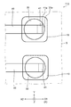
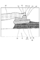
図1(a)及び図1(b)は、第1の実施形態に係る半導体装置の構成を例示する模式的断面図である。
すなわち、図1(b)は、半導体装置の概要を例示しており、図1(a)は、図1(b)の1B部分を拡大して例示している。
図2は、第1の実施形態に係る半導体装置の構成を例示する模式的平面図である。
図2は、図1(b)の1B部分を拡大して例示している。
第1電極10は、半導体素子5に電気的に接続される。半導体素子5には、例えばメモリなどの半導体チップが用いられる。ただし、実施形態はこれに限らず、半導体素子5には任意の半導体チップを用いることができる。
ワイヤ40は、ボール部30と第2電極20とを接続する。すなわち、ワイヤ40の一端は、ボール部30と接し、ワイヤ40の他端は、第2電極20と接する。
ボール部30及びワイヤ40には、例えば金などの材料が用いられる。
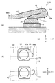
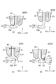
すなわち、図3(a)は模式的断面図であり、図3(b)は模式的平面図である。
図3(a)及び図3(b)に表したように、参考例の半導体装置119においては、ワイヤ40の第2電極20とは反対側の端の2重折り返し部49の厚さ49tは、ワイヤ40の径40dよりも厚い。半導体装置119における2重折り返し部49は、ワイヤ40のうちでボール部30からX1方向に向けて延在する部分と、ワイヤ40のうちでX1方向の端から折り返してX2方向に向けて延在する部分と、が重なった部分である。このため、半導体装置119における2重折り返し部49の厚さ49tは、ワイヤ40の径40dの約2倍程度の厚さである。
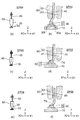
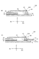
図4(a)〜図4(f)、図5(a)〜図5(f)、図6(a)〜図6(f)、及び、図7(a)〜図7(e)は、第1の実施形態に係る半導体装置の製造方法を例示する模式図である。
図4(a)、図4(c)、図4(e)、図5(a)、図5(c)、図5(e)、図6(a)、図6(c)、及び、図6(e)は、ステップSP01〜SP09の各工程におけるキャピラリ60の状態及び動作を例示している。図4(b)、図4(d)、図4(f)、図5(b)、図5(d)、図5(f)、図6(b)、図6(d)、及び、図6(f)は、ステップSP01〜SP09の各工程におけるキャピラリ60、第1電極10、ボール部30及びワイヤ40の状態を例示している。
図7(a)〜図7(e)は、ステップSP10〜SP14におけるキャピラリ60の状態及び動作を例示している。なお、図4(d)には、断面図の他に、ボール部30の平面図も描かれている。
台座部31の径31dは、例えば50μm〜60μmであり、上部32の径32dは、例えば台座部31の径31dよりも5μm〜10μm程度小さくなる。ただし、実施形態はこれに限らず、台座部31の径31d及び上部32の径32dは任意である。
その後、図7(b)に表したように、キャピラリ60を、第1電極10に対して相対的にX1方向に移動させる(ステップSP11)。
その後、図7(c)に表したように、キャピラリ60を、さらに上昇させる(ステップSP12)。
その後、図7(d)に表したように、キャピラリ60を第2電極20(図示しない)へ向けてX2方向に沿って移動させる(ステップSP13)。
そして、図7(e)に表したように、キャピラリ60を第2電極20に向けて近接させ、ワイヤ40のボール部30とは反対側の端を第2電極20に接続する(ステップSP14)。
これにより、図1(a)、図1(b)及び図2に例示した半導体装置110が製造される。
すなわち、図8(a)は、実施形態に係る半導体装置110におけるキャピラリ60の動きを模式的に例示し、図8(b)は、参考例の半導体装置119におけるキャピラリ60の動きを模式的に例示している。
図8(a)に表したように、半導体装置110の製造においては、キャピラリ60を、第1電極10に対して相対的にX1方向に移動させた(ステップSP04)後に、キャピラリ60を降下させて第2電極側先端62によるワイヤ40の変形(ステップSP05)が実施される。さらに、キャピラリ60を第1電極10に対して相対的にX2方向に移動させた(ステップSP07)後に、キャピラリ60を降下させて第1電極側先端61によるワイヤ40の変形(ステップSP08)が実施される。そして、その後、ワイヤ40が第2電極20に接続される(ステップSP14)。上記のキャピラリ60のX1方向に向けた移動、及び、X2方向に向けた移動の距離は、ボール部30の範囲内である。このように、半導体装置110の製造においては、1回目のワイヤ40の押しつぶし(ステップSP05)と、2回目のワイヤ40の押しつぶし(ステップSP08)と、が実施される。
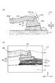
図9(a)及び図9(b)は、実施例に係る半導体装置の構成を例示する模式図である。
すなわち、図9(a)は模式的断面図であり、図9(b)は模式的斜視図である。図9(b)は、分かり易いように、実施例に係る半導体装置111の走査電子顕微鏡(SEM)写真像を基に、各要素の外形を線で描いたものである。
図9(a)及び図9(b)に表したように、本実施形態に係る実施例の半導体装置111においては、半導体素子5に電気的に接触する第1電極10として、半導体素子5の上に設けられたパッド電極11が用いられている。そして、パッド電極11とボール部30との間に下層接続部14が設けられている。下層接続部14は、パッド電極11に接続された下層ワイヤ13と、下層ワイヤ13の下層終端部12と、を含む。下層ワイヤ13は、パッド電極11と、パッド電極11よりもX1方向に設けられている別の電極(図示しない)と、を接続している。
図10は、図9(b)を拡大したものである。
さらに、境界の線Ldは、ボール部30の凸部30cの側面とワイヤ40との境界に対応する。
図11(a)〜図11(d)は、実施例に係る半導体装置の製造方法を例示する模式図である。
すなわち、図11(a)、図11(b)、図11(c)及び図11(d)は、ステップSP05、SP06、SP07及びSP08におけるワイヤ40の状態を模式的に示している。
第2の実施の形態においては、積層された半導体チップが用いられる。そして、ワイヤ40は、積層された半導体チップどうしを電気的に接続する。
図12(a)に表したように、本実施形態に係る半導体装置120は、既に説明した第1半導体素子(半導体素子5)と、第1電極10と、第2電極20と、ボール部30と、ワイヤ40と、に加え、第2半導体素子6(半導体チップ)をさらに備える。第2半導体素子6には、例えばメモリなどの半導体チップが用いられる。ただし、実施形態はこれに限らず、第2半導体素子6には任意の半導体チップを用いることができる。
ワイヤ40は、第1電極10の上方と、第2電極20の上方と、の間において、第1半導体素子(半導体素子5)の主面及び第2半導体素子6の主面に対して実質的に平行である。
すなわち、半導体装置121は、下層ワイヤ13をさらに備える。下層ワイヤ13の一端(下層終端部12)は、ボール部30と第1電極10との間に接続される。下層ワイヤ13は、第1電極10から、第2電極20から第1電極10に向かう方向(X1方向)に向けて延出する。
図13(a)〜図13(d)は、実施例に係る半導体装置の構成を例示する模式図である。
図13(a)は、実施例に係る半導体装置122の構成の概要を例示する模式的断面図であり、図13(b)は、図13(a)の一部13Aを拡大した模式的斜視図であり、図13(c)は、図13(b)の一部13Bを拡大した模式的斜視図であり、図13(d)は、図13(c)の一部13Cを拡大した模式的斜視図である。なお、図13(b)、図13(c)及び図13(d)は、半導体装置122のSEM写真像を基に、各要素の外形を描いたものである。
また、図13(b)に表したように、下層ワイヤ13の第1電極10に接続された部分から延出する部分は、第1電極10の主面に対して実質的に平行である。
図14(a)は、本実施形態に係る別の実施例の半導体装置123の一部を拡大した模式的斜視図であり、図14(b)は、図14(a)の一部14Aを拡大した模式的斜視図である。図14(a)及び図14(b)は、半導体装置123のSEM写真像を基に、各要素の外形を描いたものである。
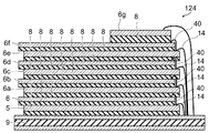
図15に表したように、本実施形態に係る別の半導体装置124は、第1半導体素子(半導体素子5)が基板9の上に設けられ、その上に第2半導体素子6が積層され、その上に第3〜第9半導体素子6a〜6gが順次積層されている。そして、半導体素子の相互がワイヤ40によって接続されている。
このように、半導体装置において、設けられる半導体素子の数は、任意である。
第3の実施形態は、半導体装置の製造方法である。
図16は、第3の実施形態に係る半導体装置の製造方法を例示するフローチャート図である。
図16に表したように、半導体素子5に電気的に接続された第1電極10の上方に配置されたキャピラリ60を下降させて、キャピラリ60に保持されたワイヤ40の先端のボール30aを第1電極10に押し付けて、第1電極10上にワイヤ40に接続されたボール部を形成する(ステップS110)。
すなわち、ステップSP01及びステップSP02を実施する。
すなわち、ステップSP03〜ステップSP05を実施する。ステップS120(ステップSP05)において、ボール部30を第1電極10に押し付けて、ボール部30も変形させても良い。
すなわち、ステップSP06〜ステップSP08を実施する。ステップS130(ステップSP08)において、ボール部30を第1電極10に押し付けて、ボール部30も変形させても良い。
すなわち、例えば、ステップSP09〜ステップSP14を実施する。
第4の実施形態は、半導体装置の製造装置である。
図4(a)に表したように、本実施形態に係る製造装置は、ワイヤ40を供給するキャピラリ60と、キャピラリ60の位置を制御する制御部80と、を備える。
また、各具体例のいずれか2つ以上の要素を技術的に可能な範囲で組み合わせたものも、本発明の要旨を包含する限り本発明の範囲に含まれる。
Claims (7)
- 第1半導体素子と、
前記第1半導体素子に電気的に接続された第1電極と、
第2電極と、
前記第1電極の上に設けられたボール部と、
前記ボール部と前記第2電極とを接続するワイヤと、
を備え、
前記ワイヤの前記第2電極とは反対側の端の折り返し部分の厚さは、前記ワイヤの径よりも薄いことを特徴とする半導体装置。 - 前記折り返し部分の前記第2電極とは反対の側の端は、前記ボール部の前記第2電極とは反対の側の端よりも前記第2電極に近いことを特徴とする請求項1記載の半導体装置。
- 前記ワイヤは、前記ワイヤの前記ボール部の上方の部分に設けられた凹部を有し、
前記ワイヤの前記ボール部に近接した部分は、上方に向けて延出していることを特徴とする請求項1または2に記載の半導体装置。 - 前記第1半導体素子の前記第1電極が設けられる側の主面に積層された第2半導体素子をさらに備え、
前記第2電極は、前記第2半導体素子に電気的に接続され、
前記ワイヤは、前記第1電極の上方と、前記第2電極の上方と、の間において、前記第1の主面及び前記第2半導体素子の主面に対して実質的に平行であることを特徴とする請求項1〜3のいずれか1つに記載の半導体装置。 - 一端が前記ボール部と前記第1電極との間に接続され、前記第1電極から、前記第2電極から前記第1電極に向かう方向に向けて延出する下層ワイヤをさらに備えたことを特徴とする請求項4記載の半導体装置。
- 半導体素子に電気的に接続された第1電極の上方に配置されたキャピラリを下降させて、前記キャピラリに保持されたワイヤの先端のボールを前記第1電極に押し付けて、前記第1電極上に前記ワイヤに接続されたボール部を形成し、
前記キャピラリを上昇させて前記キャピラリを第2電極から前記第1電極に向かう第1方向に向けて移動させた後に、前記キャピラリの前記第2電極の側の第2電極側先端で、前記ワイヤを前記第1電極に向けて加圧して前記ワイヤを変形させることにより、前記ワイヤの径よりも細い径を有する部分を形成し、
前記キャピラリを上昇させて前記キャピラリを前記第1電極から前記第2電極に向かう第2方向に向けて移動させた後に、前記キャピラリの前記第2電極側先端に対向する第1電極側先端で前記ワイヤを前記第1電極に向けて加圧して前記ワイヤを変形させて、前記ワイヤの前記第2電極とは反対の端に、前記部分に基づく、前記ワイヤの前記径よりも薄い厚さを有する折り返し部分を形成し、
前記ワイヤの前記ボール部とは反対側の端を前記第2電極に接続することを特徴とする半導体装置の製造方法。 - ワイヤを供給するキャピラリと、
前記キャピラリの位置を制御する制御部と、
を備え、
前記制御部は、
半導体素子に電気的に接続された第1電極の上方に前記キャピラリを配置した後、前記キャピラリを下降させて、前記キャピラリに保持された前記ワイヤの先端のボールを前記第1電極に押し付けて、前記第1電極上に前記ワイヤに接続されたボール部を形成し、
前記キャピラリを上昇させて前記キャピラリを第2電極から前記第1電極に向かう第1方向に向けて移動させた後に、前記キャピラリの前記第2電極の側の第2電極側先端で、前記ワイヤを前記第1電極に向けて加圧して前記ワイヤを変形させることにより、前記ワイヤの径よりも細い径を有する部分を形成させ、
前記キャピラリを上昇させて前記キャピラリを前記第1電極から前記第2電極に向かう第2方向に向けて移動させた後に、前記キャピラリの前記第2電極側先端に対向する第1電極側先端で、前記ワイヤを前記第1電極に向けて加圧して前記ワイヤを変形させて、前記ワイヤの前記第2電極とは反対の端に、前記部分に基づく、前記ワイヤの前記径よりも薄い厚さを有する折り返し部分を形成させ、
前記ワイヤの前記ボール部とは反対側の端を前記第2電極に接続させることを特徴とする半導体装置の製造装置。
Priority Applications (4)
| Application Number | Priority Date | Filing Date | Title |
|---|---|---|---|
| JP2010139998A JP2012004464A (ja) | 2010-06-18 | 2010-06-18 | 半導体装置、半導体装置の製造方法及び半導体装置の製造装置 |
| CN201110066789.7A CN102290391B (zh) | 2010-06-18 | 2011-03-18 | 半导体器件及其制造方法和制造装置 |
| TW100109462A TWI484613B (zh) | 2010-06-18 | 2011-03-18 | 半導體裝置、半導體裝置之製造方法及半導體裝置之製造設備 |
| US13/052,368 US8237295B2 (en) | 2010-06-18 | 2011-03-21 | Semiconductor device, method for manufacturing semiconductor device, and manufacturing apparatus for semiconductor device |
Applications Claiming Priority (1)
| Application Number | Priority Date | Filing Date | Title |
|---|---|---|---|
| JP2010139998A JP2012004464A (ja) | 2010-06-18 | 2010-06-18 | 半導体装置、半導体装置の製造方法及び半導体装置の製造装置 |
Related Child Applications (1)
| Application Number | Title | Priority Date | Filing Date |
|---|---|---|---|
| JP2014085372A Division JP2014140074A (ja) | 2014-04-17 | 2014-04-17 | 半導体装置 |
Publications (2)
| Publication Number | Publication Date |
|---|---|
| JP2012004464A true JP2012004464A (ja) | 2012-01-05 |
| JP2012004464A5 JP2012004464A5 (ja) | 2012-10-11 |
Family
ID=45327935
Family Applications (1)
| Application Number | Title | Priority Date | Filing Date |
|---|---|---|---|
| JP2010139998A Pending JP2012004464A (ja) | 2010-06-18 | 2010-06-18 | 半導体装置、半導体装置の製造方法及び半導体装置の製造装置 |
Country Status (4)
| Country | Link |
|---|---|
| US (1) | US8237295B2 (ja) |
| JP (1) | JP2012004464A (ja) |
| CN (1) | CN102290391B (ja) |
| TW (1) | TWI484613B (ja) |
Families Citing this family (2)
| Publication number | Priority date | Publication date | Assignee | Title |
|---|---|---|---|---|
| JP2013143447A (ja) * | 2012-01-10 | 2013-07-22 | Toshiba Corp | 半導体装置の製造方法およびボンディング装置 |
| KR102621753B1 (ko) | 2018-09-28 | 2024-01-05 | 삼성전자주식회사 | 본딩 와이어, 이를 포함하는 반도체 패키지, 및 와이어 본딩 방법 |
Citations (4)
| Publication number | Priority date | Publication date | Assignee | Title |
|---|---|---|---|---|
| JPH0951011A (ja) * | 1995-08-10 | 1997-02-18 | Tanaka Denshi Kogyo Kk | 半導体チップのワイヤボンディング方法 |
| JP2005167178A (ja) * | 2003-11-10 | 2005-06-23 | Shinkawa Ltd | 半導体装置及びワイヤボンディング方法 |
| JP2010067786A (ja) * | 2008-09-10 | 2010-03-25 | Kaijo Corp | ワイヤボンディング方法、ワイヤボンディング装置及びワイヤボンディング制御プログラム |
| JP2010103403A (ja) * | 2008-10-27 | 2010-05-06 | Shinkawa Ltd | ワイヤボンディング方法 |
Family Cites Families (17)
| Publication number | Priority date | Publication date | Assignee | Title |
|---|---|---|---|---|
| US7200930B2 (en) * | 1994-11-15 | 2007-04-10 | Formfactor, Inc. | Probe for semiconductor devices |
| EP1408337A3 (en) * | 1994-11-15 | 2007-09-19 | FormFactor, Inc. | Probe card assembly |
| EP1158578B1 (en) * | 1996-10-01 | 2004-06-30 | Matsushita Electric Industrial Co., Ltd. | Integrated circuit or circuit board with bump electrode and manufacturing method thereof |
| JP2004172477A (ja) | 2002-11-21 | 2004-06-17 | Kaijo Corp | ワイヤループ形状、そのワイヤループ形状を備えた半導体装置、ワイヤボンディング方法及び半導体製造装置 |
| JP2005019493A (ja) * | 2003-06-24 | 2005-01-20 | Renesas Technology Corp | 半導体装置 |
| US7347352B2 (en) * | 2003-11-26 | 2008-03-25 | Kulicke And Soffa Industries, Inc. | Low loop height ball bonding method and apparatus |
| CN1886226A (zh) * | 2003-11-26 | 2006-12-27 | 库利克和索夫工业公司 | 低回路高度球焊方法和设备 |
| JP4298665B2 (ja) * | 2005-02-08 | 2009-07-22 | 株式会社新川 | ワイヤボンディング方法 |
| US7371676B2 (en) * | 2005-04-08 | 2008-05-13 | Micron Technology, Inc. | Method for fabricating semiconductor components with through wire interconnects |
| JP2008034567A (ja) * | 2006-07-27 | 2008-02-14 | Fujitsu Ltd | 半導体装置及びその製造方法 |
| WO2008048262A1 (en) * | 2006-10-18 | 2008-04-24 | Kulicke And Soffa Industries, Inc. | Improved conductive bumps, wire loops including the improved conductive bumps, and methods of forming the same |
| KR101143836B1 (ko) * | 2006-10-27 | 2012-05-04 | 삼성테크윈 주식회사 | 반도체 패키지 및 그 반도체 패키지의 와이어 루프 형성방법 |
| JP2008117888A (ja) * | 2006-11-02 | 2008-05-22 | Rohm Co Ltd | 電子部品、およびワイヤボンディング方法 |
| US20080197461A1 (en) * | 2007-02-15 | 2008-08-21 | Taiwan Semiconductor Manufacturing Co.,Ltd. | Apparatus for wire bonding and integrated circuit chip package |
| JP2009010064A (ja) * | 2007-06-27 | 2009-01-15 | Shinkawa Ltd | 半導体装置及びワイヤボンディング方法 |
| US7572679B2 (en) * | 2007-07-26 | 2009-08-11 | Texas Instruments Incorporated | Heat extraction from packaged semiconductor chips, scalable with chip area |
| JP4397408B2 (ja) * | 2007-09-21 | 2010-01-13 | 株式会社新川 | 半導体装置及びワイヤボンディング方法 |
-
2010
- 2010-06-18 JP JP2010139998A patent/JP2012004464A/ja active Pending
-
2011
- 2011-03-18 CN CN201110066789.7A patent/CN102290391B/zh active Active
- 2011-03-18 TW TW100109462A patent/TWI484613B/zh active
- 2011-03-21 US US13/052,368 patent/US8237295B2/en active Active
Patent Citations (4)
| Publication number | Priority date | Publication date | Assignee | Title |
|---|---|---|---|---|
| JPH0951011A (ja) * | 1995-08-10 | 1997-02-18 | Tanaka Denshi Kogyo Kk | 半導体チップのワイヤボンディング方法 |
| JP2005167178A (ja) * | 2003-11-10 | 2005-06-23 | Shinkawa Ltd | 半導体装置及びワイヤボンディング方法 |
| JP2010067786A (ja) * | 2008-09-10 | 2010-03-25 | Kaijo Corp | ワイヤボンディング方法、ワイヤボンディング装置及びワイヤボンディング制御プログラム |
| JP2010103403A (ja) * | 2008-10-27 | 2010-05-06 | Shinkawa Ltd | ワイヤボンディング方法 |
Also Published As
| Publication number | Publication date |
|---|---|
| CN102290391A (zh) | 2011-12-21 |
| CN102290391B (zh) | 2014-11-12 |
| US20110309502A1 (en) | 2011-12-22 |
| TWI484613B (zh) | 2015-05-11 |
| US8237295B2 (en) | 2012-08-07 |
| TW201201341A (en) | 2012-01-01 |
Similar Documents
| Publication | Publication Date | Title |
|---|---|---|
| JP4298665B2 (ja) | ワイヤボンディング方法 | |
| JP5220714B2 (ja) | 樹脂封止型半導体装置及びその製造方法 | |
| US7547626B2 (en) | Semiconductor package and method of forming wire loop of semiconductor package | |
| US8815732B2 (en) | Wire bonding method and semiconductor device | |
| JP2010067786A (ja) | ワイヤボンディング方法、ワイヤボンディング装置及びワイヤボンディング制御プログラム | |
| JP2014513870A (ja) | ウォータフォール・ワイヤボンディング | |
| JP2012004464A (ja) | 半導体装置、半導体装置の製造方法及び半導体装置の製造装置 | |
| US11145617B2 (en) | Semiconductor structure | |
| JP2014140074A (ja) | 半導体装置 | |
| JP2011054727A (ja) | 半導体装置、その製造方法、及びワイヤボンディング方法 | |
| JP4369401B2 (ja) | ワイヤボンディング方法 | |
| KR20110062482A (ko) | 본딩 구조물의 형성 방법 | |
| EP2471624A1 (en) | Continuous wire bonding | |
| JP4361336B2 (ja) | 半導体装置の製造方法 | |
| JP2005167178A (ja) | 半導体装置及びワイヤボンディング方法 | |
| JP4215689B2 (ja) | ワイヤボンディング方法及びバンプ形成方法 | |
| KR102072527B1 (ko) | 반도체 장치 및 그 제조 방법 | |
| JP2007266062A (ja) | 半導体装置の製造方法 | |
| CN217606848U (zh) | 器件连接装置、封装体及电子装置 | |
| JP2007281509A (ja) | 半導体装置 | |
| JP2006196597A (ja) | 電子装置およびその製造方法 | |
| JP5048990B2 (ja) | 半導体装置及びその製造方法 | |
| JP2010073747A (ja) | ワイヤボンディング方法及び半導体装置 | |
| JP4887854B2 (ja) | バンプの形成方法およびバンプ | |
| JP2008135578A (ja) | ワイヤボンディング方法 |
Legal Events
| Date | Code | Title | Description |
|---|---|---|---|
| A521 | Request for written amendment filed |
Free format text: JAPANESE INTERMEDIATE CODE: A523 Effective date: 20120821 |
|
| A621 | Written request for application examination |
Free format text: JAPANESE INTERMEDIATE CODE: A621 Effective date: 20120821 |
|
| A131 | Notification of reasons for refusal |
Free format text: JAPANESE INTERMEDIATE CODE: A131 Effective date: 20130326 |
|
| A977 | Report on retrieval |
Free format text: JAPANESE INTERMEDIATE CODE: A971007 Effective date: 20130328 |
|
| A131 | Notification of reasons for refusal |
Free format text: JAPANESE INTERMEDIATE CODE: A131 Effective date: 20131111 |
|
| A521 | Request for written amendment filed |
Free format text: JAPANESE INTERMEDIATE CODE: A523 Effective date: 20131225 |
|
| A02 | Decision of refusal |
Free format text: JAPANESE INTERMEDIATE CODE: A02 Effective date: 20140117 |
|
| A521 | Request for written amendment filed |
Free format text: JAPANESE INTERMEDIATE CODE: A523 Effective date: 20140417 |
|
| A911 | Transfer to examiner for re-examination before appeal (zenchi) |
Free format text: JAPANESE INTERMEDIATE CODE: A911 Effective date: 20140428 |
|
| A912 | Re-examination (zenchi) completed and case transferred to appeal board |
Free format text: JAPANESE INTERMEDIATE CODE: A912 Effective date: 20140606 |
|
| RD02 | Notification of acceptance of power of attorney |
Free format text: JAPANESE INTERMEDIATE CODE: A7422 Effective date: 20150216 |
|
| RD04 | Notification of resignation of power of attorney |
Free format text: JAPANESE INTERMEDIATE CODE: A7424 Effective date: 20150218 |
|
| A521 | Request for written amendment filed |
Free format text: JAPANESE INTERMEDIATE CODE: A523 Effective date: 20150714 |