JP2011054596A - Ccdイメージセンサ - Google Patents
Ccdイメージセンサ Download PDFInfo
- Publication number
- JP2011054596A JP2011054596A JP2009199389A JP2009199389A JP2011054596A JP 2011054596 A JP2011054596 A JP 2011054596A JP 2009199389 A JP2009199389 A JP 2009199389A JP 2009199389 A JP2009199389 A JP 2009199389A JP 2011054596 A JP2011054596 A JP 2011054596A
- Authority
- JP
- Japan
- Prior art keywords
- image sensor
- ccd image
- pixel
- transfer gate
- width
- Prior art date
- Legal status (The legal status is an assumption and is not a legal conclusion. Google has not performed a legal analysis and makes no representation as to the accuracy of the status listed.)
- Pending
Links
Images


Classifications
-
- H—ELECTRICITY
- H10—SEMICONDUCTOR DEVICES; ELECTRIC SOLID-STATE DEVICES NOT OTHERWISE PROVIDED FOR
- H10F—INORGANIC SEMICONDUCTOR DEVICES SENSITIVE TO INFRARED RADIATION, LIGHT, ELECTROMAGNETIC RADIATION OF SHORTER WAVELENGTH OR CORPUSCULAR RADIATION
- H10F39/00—Integrated devices, or assemblies of multiple devices, comprising at least one element covered by group H10F30/00, e.g. radiation detectors comprising photodiode arrays
- H10F39/10—Integrated devices
- H10F39/12—Image sensors
- H10F39/15—Charge-coupled device [CCD] image sensors
- H10F39/151—Geometry or disposition of pixel elements, address lines or gate electrodes
Landscapes
- Solid State Image Pick-Up Elements (AREA)
- Transforming Light Signals Into Electric Signals (AREA)
Priority Applications (2)
| Application Number | Priority Date | Filing Date | Title |
|---|---|---|---|
| JP2009199389A JP2011054596A (ja) | 2009-08-31 | 2009-08-31 | Ccdイメージセンサ |
| US12/848,503 US8259207B2 (en) | 2009-08-31 | 2010-08-02 | CCD image sensor |
Applications Claiming Priority (1)
| Application Number | Priority Date | Filing Date | Title |
|---|---|---|---|
| JP2009199389A JP2011054596A (ja) | 2009-08-31 | 2009-08-31 | Ccdイメージセンサ |
Publications (2)
| Publication Number | Publication Date |
|---|---|
| JP2011054596A true JP2011054596A (ja) | 2011-03-17 |
| JP2011054596A5 JP2011054596A5 (https=) | 2012-04-05 |
Family
ID=43624368
Family Applications (1)
| Application Number | Title | Priority Date | Filing Date |
|---|---|---|---|
| JP2009199389A Pending JP2011054596A (ja) | 2009-08-31 | 2009-08-31 | Ccdイメージセンサ |
Country Status (2)
| Country | Link |
|---|---|
| US (1) | US8259207B2 (https=) |
| JP (1) | JP2011054596A (https=) |
Cited By (2)
| Publication number | Priority date | Publication date | Assignee | Title |
|---|---|---|---|---|
| JP2014525673A (ja) * | 2011-08-26 | 2014-09-29 | イー・2・ブイ・セミコンダクターズ | ピクセル・グループ化イメージ・センサー |
| JP2019046995A (ja) * | 2017-09-04 | 2019-03-22 | 浜松ホトニクス株式会社 | 固体撮像装置 |
Families Citing this family (2)
| Publication number | Priority date | Publication date | Assignee | Title |
|---|---|---|---|---|
| JP2013175610A (ja) * | 2012-02-27 | 2013-09-05 | Toshiba Corp | 固体撮像素子 |
| JP6348272B2 (ja) * | 2013-11-05 | 2018-06-27 | 浜松ホトニクス株式会社 | 電荷結合素子及びその製造方法、並びに固体撮像装置 |
Citations (3)
| Publication number | Priority date | Publication date | Assignee | Title |
|---|---|---|---|---|
| JPH05283666A (ja) * | 1992-03-30 | 1993-10-29 | Sony Corp | 固体撮像素子 |
| JPH05347401A (ja) * | 1992-06-15 | 1993-12-27 | Matsushita Electron Corp | 固体撮像素子 |
| JP2002231926A (ja) * | 2001-02-01 | 2002-08-16 | Fuji Photo Film Co Ltd | ラインセンサおよびそれを用いた放射線画像情報読取装置 |
Family Cites Families (9)
| Publication number | Priority date | Publication date | Assignee | Title |
|---|---|---|---|---|
| JPS58212176A (ja) * | 1982-06-02 | 1983-12-09 | Nec Corp | 電荷転送装置 |
| KR930011473B1 (ko) * | 1990-10-16 | 1993-12-08 | 삼성전자 주식회사 | 좁은 채널효과를 가지는 의사이상 전하 결합소자 |
| JPH05283670A (ja) * | 1992-04-03 | 1993-10-29 | Sony Corp | 固体撮像素子及び固体撮像素子の電荷読出し方法 |
| KR0136934B1 (ko) | 1994-02-23 | 1998-04-24 | 문정환 | 선형 고체영상소자 |
| US5514886A (en) * | 1995-01-18 | 1996-05-07 | Eastman Kodak Company | Image sensor with improved output region for superior charge transfer characteristics |
| US5705836A (en) * | 1995-05-22 | 1998-01-06 | Dalsa, Inc. | Efficient charge transfer structure in large pitch charge coupled device |
| US6646682B1 (en) * | 1998-12-18 | 2003-11-11 | Syscan (Shenzhen) Technology Co., Limited | Linear tri-color image sensors |
| JP4258875B2 (ja) | 1999-02-15 | 2009-04-30 | 株式会社ニコン | 光電変換素子及び光電変換装置 |
| JP3928840B2 (ja) * | 2001-02-01 | 2007-06-13 | 富士フイルム株式会社 | 固体撮像装置 |
-
2009
- 2009-08-31 JP JP2009199389A patent/JP2011054596A/ja active Pending
-
2010
- 2010-08-02 US US12/848,503 patent/US8259207B2/en not_active Expired - Fee Related
Patent Citations (3)
| Publication number | Priority date | Publication date | Assignee | Title |
|---|---|---|---|---|
| JPH05283666A (ja) * | 1992-03-30 | 1993-10-29 | Sony Corp | 固体撮像素子 |
| JPH05347401A (ja) * | 1992-06-15 | 1993-12-27 | Matsushita Electron Corp | 固体撮像素子 |
| JP2002231926A (ja) * | 2001-02-01 | 2002-08-16 | Fuji Photo Film Co Ltd | ラインセンサおよびそれを用いた放射線画像情報読取装置 |
Cited By (3)
| Publication number | Priority date | Publication date | Assignee | Title |
|---|---|---|---|---|
| JP2014525673A (ja) * | 2011-08-26 | 2014-09-29 | イー・2・ブイ・セミコンダクターズ | ピクセル・グループ化イメージ・センサー |
| JP2019046995A (ja) * | 2017-09-04 | 2019-03-22 | 浜松ホトニクス株式会社 | 固体撮像装置 |
| US11942506B2 (en) | 2017-09-04 | 2024-03-26 | Hamamatsu Photonics K.K. | Solid state imaging device |
Also Published As
| Publication number | Publication date |
|---|---|
| US8259207B2 (en) | 2012-09-04 |
| US20110050971A1 (en) | 2011-03-03 |
Similar Documents
| Publication | Publication Date | Title |
|---|---|---|
| JP5864990B2 (ja) | 固体撮像装置およびカメラ | |
| KR101683307B1 (ko) | 고체 촬상 장치, 고체 촬상 장치의 제조 방법, 및 전자 기기 | |
| JP4756839B2 (ja) | 固体撮像装置及びカメラ | |
| JP5767465B2 (ja) | 固体撮像装置およびその製造方法ならびにカメラ | |
| JP2009253149A (ja) | 光電変換装置及びそれを用いた撮像システム | |
| CN103688359B (zh) | 固态成像装置及其驱动方法、固态成像装置的制造方法以及电子信息设备 | |
| CN102956658A (zh) | 固态成像设备、固态成像设备的制造方法及电子设备 | |
| JP2016152374A (ja) | 光電変換装置 | |
| CN100429780C (zh) | 固体摄像装置 | |
| JP2004273640A (ja) | 固体撮像素子及びその製造方法 | |
| JP4474962B2 (ja) | 裏面照射型固体撮像素子、電子機器モジュール及びカメラモジュール | |
| JP5036709B2 (ja) | Cmos能動画素センサの増幅器を共有した画素 | |
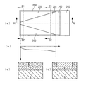
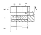
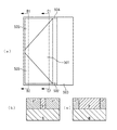
| JP2011054596A (ja) | Ccdイメージセンサ | |
| US9231021B2 (en) | Image pickup apparatus, image pickup system, and image pickup apparatus manufacturing method | |
| JP4122960B2 (ja) | 固体撮像素子 | |
| JP2005109021A (ja) | 固体撮像素子 | |
| JP2012124213A (ja) | 固体撮像素子 | |
| JP2011258598A (ja) | 固体撮像素子及びその製造方法、並びに撮像機器 | |
| JP6178835B2 (ja) | 固体撮像装置およびカメラ | |
| JP5701344B2 (ja) | 光電変換装置及びそれを用いた撮像システム | |
| JP5725232B2 (ja) | 固体撮像装置及びカメラ | |
| KR100769563B1 (ko) | 누설 전류를 감소시킨 이미지 센서 | |
| JP2017212456A (ja) | 固体撮像装置およびカメラ | |
| JP2017163607A (ja) | 固体撮像装置及び電子機器 | |
| JP4696596B2 (ja) | 撮像素子及び撮像素子の製造方法 |
Legal Events
| Date | Code | Title | Description |
|---|---|---|---|
| A521 | Request for written amendment filed |
Free format text: JAPANESE INTERMEDIATE CODE: A523 Effective date: 20120217 |
|
| A621 | Written request for application examination |
Free format text: JAPANESE INTERMEDIATE CODE: A621 Effective date: 20120217 |
|
| A977 | Report on retrieval |
Free format text: JAPANESE INTERMEDIATE CODE: A971007 Effective date: 20130415 |
|
| A131 | Notification of reasons for refusal |
Free format text: JAPANESE INTERMEDIATE CODE: A131 Effective date: 20130417 |
|
| A02 | Decision of refusal |
Free format text: JAPANESE INTERMEDIATE CODE: A02 Effective date: 20130809 |