JP2010093220A - 隔離カバーを備える回路板及びその組立方法 - Google Patents
隔離カバーを備える回路板及びその組立方法 Download PDFInfo
- Publication number
- JP2010093220A JP2010093220A JP2009032693A JP2009032693A JP2010093220A JP 2010093220 A JP2010093220 A JP 2010093220A JP 2009032693 A JP2009032693 A JP 2009032693A JP 2009032693 A JP2009032693 A JP 2009032693A JP 2010093220 A JP2010093220 A JP 2010093220A
- Authority
- JP
- Japan
- Prior art keywords
- circuit board
- localization
- isolation cover
- ground
- isolation
- Prior art date
- Legal status (The legal status is an assumption and is not a legal conclusion. Google has not performed a legal analysis and makes no representation as to the accuracy of the status listed.)
- Granted
Links
- 238000002955 isolation Methods 0.000 title claims abstract description 66
- 238000000034 method Methods 0.000 title claims abstract description 37
- 230000004807 localization Effects 0.000 claims description 55
- PXHVJJICTQNCMI-UHFFFAOYSA-N Nickel Chemical compound [Ni] PXHVJJICTQNCMI-UHFFFAOYSA-N 0.000 claims description 6
- 230000000149 penetrating effect Effects 0.000 claims description 6
- 238000007747 plating Methods 0.000 claims description 4
- RYGMFSIKBFXOCR-UHFFFAOYSA-N Copper Chemical compound [Cu] RYGMFSIKBFXOCR-UHFFFAOYSA-N 0.000 claims description 3
- ATJFFYVFTNAWJD-UHFFFAOYSA-N Tin Chemical compound [Sn] ATJFFYVFTNAWJD-UHFFFAOYSA-N 0.000 claims description 3
- 229910052802 copper Inorganic materials 0.000 claims description 3
- 239000010949 copper Substances 0.000 claims description 3
- 229910052759 nickel Inorganic materials 0.000 claims description 3
- 229910052718 tin Inorganic materials 0.000 claims description 3
- 239000011135 tin Substances 0.000 claims description 3
- 238000005476 soldering Methods 0.000 description 9
- 238000005516 engineering process Methods 0.000 description 7
- 230000000694 effects Effects 0.000 description 6
- 229910000679 solder Inorganic materials 0.000 description 5
- 238000004519 manufacturing process Methods 0.000 description 4
- 238000003825 pressing Methods 0.000 description 4
- 230000033228 biological regulation Effects 0.000 description 3
- 238000013461 design Methods 0.000 description 3
- 238000012423 maintenance Methods 0.000 description 3
- 230000005540 biological transmission Effects 0.000 description 2
- 238000004891 communication Methods 0.000 description 2
- 238000011161 development Methods 0.000 description 2
- 206010035148 Plague Diseases 0.000 description 1
- 241000607479 Yersinia pestis Species 0.000 description 1
- 230000000903 blocking effect Effects 0.000 description 1
- 238000010586 diagram Methods 0.000 description 1
- 230000017525 heat dissipation Effects 0.000 description 1
- 230000008676 import Effects 0.000 description 1
- 238000013021 overheating Methods 0.000 description 1
- 238000000926 separation method Methods 0.000 description 1
Images


Classifications
-
- H—ELECTRICITY
- H05—ELECTRIC TECHNIQUES NOT OTHERWISE PROVIDED FOR
- H05K—PRINTED CIRCUITS; CASINGS OR CONSTRUCTIONAL DETAILS OF ELECTRIC APPARATUS; MANUFACTURE OF ASSEMBLAGES OF ELECTRICAL COMPONENTS
- H05K1/00—Printed circuits
- H05K1/02—Details
-
- H—ELECTRICITY
- H05—ELECTRIC TECHNIQUES NOT OTHERWISE PROVIDED FOR
- H05K—PRINTED CIRCUITS; CASINGS OR CONSTRUCTIONAL DETAILS OF ELECTRIC APPARATUS; MANUFACTURE OF ASSEMBLAGES OF ELECTRICAL COMPONENTS
- H05K9/00—Screening of apparatus or components against electric or magnetic fields
-
- H—ELECTRICITY
- H05—ELECTRIC TECHNIQUES NOT OTHERWISE PROVIDED FOR
- H05K—PRINTED CIRCUITS; CASINGS OR CONSTRUCTIONAL DETAILS OF ELECTRIC APPARATUS; MANUFACTURE OF ASSEMBLAGES OF ELECTRICAL COMPONENTS
- H05K9/00—Screening of apparatus or components against electric or magnetic fields
- H05K9/0007—Casings
- H05K9/002—Casings with localised screening
- H05K9/0039—Galvanic coupling of ground layer on printed circuit board [PCB] to conductive casing
-
- H—ELECTRICITY
- H05—ELECTRIC TECHNIQUES NOT OTHERWISE PROVIDED FOR
- H05K—PRINTED CIRCUITS; CASINGS OR CONSTRUCTIONAL DETAILS OF ELECTRIC APPARATUS; MANUFACTURE OF ASSEMBLAGES OF ELECTRICAL COMPONENTS
- H05K9/00—Screening of apparatus or components against electric or magnetic fields
- H05K9/0007—Casings
- H05K9/002—Casings with localised screening
- H05K9/0022—Casings with localised screening of components mounted on printed circuit boards [PCB]
- H05K9/0024—Shield cases mounted on a PCB, e.g. cans or caps or conformal shields
- H05K9/0026—Shield cases mounted on a PCB, e.g. cans or caps or conformal shields integrally formed from metal sheet
-
- Y—GENERAL TAGGING OF NEW TECHNOLOGICAL DEVELOPMENTS; GENERAL TAGGING OF CROSS-SECTIONAL TECHNOLOGIES SPANNING OVER SEVERAL SECTIONS OF THE IPC; TECHNICAL SUBJECTS COVERED BY FORMER USPC CROSS-REFERENCE ART COLLECTIONS [XRACs] AND DIGESTS
- Y10—TECHNICAL SUBJECTS COVERED BY FORMER USPC
- Y10T—TECHNICAL SUBJECTS COVERED BY FORMER US CLASSIFICATION
- Y10T29/00—Metal working
- Y10T29/49—Method of mechanical manufacture
- Y10T29/49002—Electrical device making
- Y10T29/49117—Conductor or circuit manufacturing
- Y10T29/49124—On flat or curved insulated base, e.g., printed circuit, etc.
Landscapes
- Engineering & Computer Science (AREA)
- Microelectronics & Electronic Packaging (AREA)
- Shielding Devices Or Components To Electric Or Magnetic Fields (AREA)
- Casings For Electric Apparatus (AREA)
- Structures For Mounting Electric Components On Printed Circuit Boards (AREA)
- Mounting Of Printed Circuit Boards And The Like (AREA)
- Coupling Device And Connection With Printed Circuit (AREA)
- Telephone Set Structure (AREA)
Abstract
【解決手段】隔離カバーを備える回路板及びその組立方法において、回路板は回路板本体及び回路板本体に設ける隔離カバーを備える。前記回路板本体と隔離カバーは、相対する複数の第一定位部及び第二定位部を備え、しかも各第一定位部の最低一方側にはアース部を設ける。前記隔離カバーは、回路板本体の第一表面を被覆する状態で配置され、各第二定位部は各第一定位部を経て回路板本体の第二表面に貫通し、且つ各第二定位部の末端は各アース部にプレスフィットされて組立てが完成する。
【選択図】図3
Description
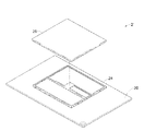
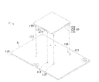
11 回路板本体
111 第一表面
113 第二表面
1131 凹部
115 第一定位部
117 アース部
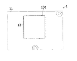
13 隔離カバー
131 カバー本体
133 第二定位部
135 開口
2 回路板
2' 回路板
20 回路板本体
22 隔離カバー
24 下部フレーム
26 上蓋体
Claims (10)
- 隔離カバーを備える回路板において、
対称となる第一表面と第二表面、第一表面と第二表面を貫通する複数の第一定位部、及び、第二表面に設け且つ各第一定位部の最低一方側に位置する複数のアース部を備える回路板本体と、
対応する各第一定位部を貫通する複数の第二定位部を備え、しかも各第二定位部の末端が対応するアース部にプレスフィットされる隔離カバーとにより構成されることを特徴とする隔離カバーを備える回路板。 - 前記第一定位部は導通孔であり、アース部はアースパッドであることを特徴とする請求項1記載の隔離カバーを備える回路板。
- 前記隔離カバーはカバー本体、及びカバー本体のエッジに位置し下方向に延伸する各第二定位部を備え、前記第二定位部はカバー本体の角のエッジに位置することを特徴とする請求項1記載の隔離カバーを備える回路板。
- 前記第二定位部の長さは第一定位部に対応するアース部を加えた総長と等しいかそれより短く、前記第二定位部の数量は第一定位部の数量に等しいかそれより少ないことを特徴とする請求項1記載の隔離カバーを備える回路板。
- 前記第二定位部の末端はアース部に平たく密着することを特徴とする請求項1記載の隔離カバーを備える回路板。
- 隔離カバーを備える回路板の組立方法において、
対称となる第一表面と第二表面、第一表面と第二表面を貫通する複数の第一定位部、及び第二表面に設け且つ各第一定位部の最低一方側に位置する複数のアース部を備える回路板本体と、
それぞれが各第一定位部に対応する複数の第二定位部を備える隔離カバーにより構成され、
前記隔離カバーを第一表面に被覆する状態で配置し、各第二定位部は各第一定位部を経て第二表面に貫通し、
各第二定位部の末端はそれに対応するアース部に接触させるまで折り曲げることを特徴とする隔離カバーを備える回路板の組立方法。 - 前記第二定位部は先に曲げ、更にそれに対応するアース部に接触するまで平たくプレスすることを特徴とする請求項6記載の隔離カバーを備える回路板の組立方法。
- 前記第二定位部を対応するアース部に接触するまで直接平たくプレスすることを特徴とする請求項6記載の隔離カバーを備える回路板の組立方法。
- 前記第二定位部の末端を前記アース部に平たく密着させることを特徴とする請求項6記載の隔離カバーを備える回路板の組立方法。
- 前記第一定位部は導通孔であり、しかも各第一定位部は銅、スズ、ニッケルで組成したグループから選択した何れか一つのメッキ層によってメッキすることを特徴とする請求項6記載の隔離カバーを備える回路板の組立方法。
Applications Claiming Priority (2)
| Application Number | Priority Date | Filing Date | Title |
|---|---|---|---|
| TW097139173 | 2008-10-13 | ||
| TW097139173A TWI375509B (en) | 2008-10-13 | 2008-10-13 | A circuit board having an isolation cover and a method for assembling |
Publications (2)
| Publication Number | Publication Date |
|---|---|
| JP2010093220A true JP2010093220A (ja) | 2010-04-22 |
| JP4755265B2 JP4755265B2 (ja) | 2011-08-24 |
Family
ID=40433332
Family Applications (1)
| Application Number | Title | Priority Date | Filing Date |
|---|---|---|---|
| JP2009032693A Expired - Fee Related JP4755265B2 (ja) | 2008-10-13 | 2009-02-16 | 隔離カバーを備える回路板及びその組立方法 |
Country Status (10)
| Country | Link |
|---|---|
| US (1) | US7999195B2 (ja) |
| JP (1) | JP4755265B2 (ja) |
| KR (1) | KR101096387B1 (ja) |
| DE (1) | DE102009001744A1 (ja) |
| ES (1) | ES2365674B1 (ja) |
| FR (1) | FR2937215B1 (ja) |
| GB (1) | GB2464329B (ja) |
| IT (1) | IT1393922B1 (ja) |
| NL (1) | NL1036864C2 (ja) |
| TW (1) | TWI375509B (ja) |
Cited By (1)
| Publication number | Priority date | Publication date | Assignee | Title |
|---|---|---|---|---|
| EP2377710A2 (en) | 2010-04-14 | 2011-10-19 | Kobelco Construction Machinery Co. Ltd. | Hybrid working machine having battery protecting function |
Families Citing this family (6)
| Publication number | Priority date | Publication date | Assignee | Title |
|---|---|---|---|---|
| JP2011077446A (ja) * | 2009-10-01 | 2011-04-14 | Sanyo Electric Co Ltd | シールドケース及び画像表示装置 |
| US8279624B2 (en) * | 2010-06-03 | 2012-10-02 | Laird Technologies, Inc. | Board level electromagnetic interference (EMI) shields with through hole latching mechanisms |
| TW201225752A (en) * | 2010-12-10 | 2012-06-16 | Askey Computer Corp | Printed circuit board grounding structure for use with communication apparatus |
| CN104837327A (zh) * | 2015-05-21 | 2015-08-12 | 小米科技有限责任公司 | 电路保护结构及电子装置 |
| TWI749887B (zh) * | 2020-11-20 | 2021-12-11 | 英業達股份有限公司 | 電子組件及伺服器 |
| CN219065845U (zh) * | 2023-01-30 | 2023-05-23 | 三赢科技(深圳)有限公司 | 镜头模组及电子装置 |
Citations (8)
| Publication number | Priority date | Publication date | Assignee | Title |
|---|---|---|---|---|
| JPS5542363U (ja) * | 1978-09-12 | 1980-03-18 | ||
| JPH04322498A (ja) * | 1991-04-23 | 1992-11-12 | Murata Mfg Co Ltd | 高周波機器 |
| JPH0582953A (ja) * | 1991-09-24 | 1993-04-02 | Sony Corp | 半田付け方法 |
| JPH07142906A (ja) * | 1993-11-15 | 1995-06-02 | Fuji Elelctrochem Co Ltd | 誘電体フィルタの蓋体取付け構造 |
| JP2000332481A (ja) * | 1999-05-25 | 2000-11-30 | Alps Electric Co Ltd | 電子機器のシールドケース |
| JP2002280787A (ja) * | 2001-03-19 | 2002-09-27 | Murata Mfg Co Ltd | 部材相互の位置決め構造 |
| JP2003174281A (ja) * | 2001-12-06 | 2003-06-20 | Murata Mfg Co Ltd | 電子部品用シールドケース |
| JP2007299996A (ja) * | 2006-05-01 | 2007-11-15 | Alps Electric Co Ltd | 回路基板の取付構造 |
Family Cites Families (12)
| Publication number | Priority date | Publication date | Assignee | Title |
|---|---|---|---|---|
| US4370515A (en) * | 1979-12-26 | 1983-01-25 | Rockwell International Corporation | Electromagnetic interference |
| US5014160A (en) * | 1989-07-05 | 1991-05-07 | Digital Equipment Corporation | EMI/RFI shielding method and apparatus |
| JPH0818265A (ja) * | 1994-06-29 | 1996-01-19 | Molex Inc | プリント回路基板上での電磁波等のシ−ルド方法 及びその為のシ−ルドカバ− |
| US5717577A (en) * | 1996-10-30 | 1998-02-10 | Ericsson, Inc. | Gasketed shield can for shielding emissions of electromagnetic energy |
| JP2001148594A (ja) * | 1999-11-19 | 2001-05-29 | Murata Mfg Co Ltd | シールドケース付き電子部品 |
| JP3792518B2 (ja) * | 2001-01-19 | 2006-07-05 | 三菱電機株式会社 | 電子回路部品のシールド構造 |
| US6781851B2 (en) * | 2002-05-30 | 2004-08-24 | Lucent Technologies Inc. | Electromagnetic interference shield |
| DE10231145A1 (de) * | 2002-07-10 | 2004-01-29 | Siemens Ag | Abschirmeinrichtung für elektronische Baugruppen auf einer Leiterplatte |
| US20040025334A1 (en) * | 2002-08-06 | 2004-02-12 | Ming Wen | Method of securely fastening a shield to a circuit board |
| JP2005136012A (ja) * | 2003-10-28 | 2005-05-26 | Murata Mfg Co Ltd | シールドケース固定構造 |
| US20080043453A1 (en) * | 2006-08-18 | 2008-02-21 | Chin-Fu Horng | Electromagnetic-shielding device |
| CN201063966Y (zh) | 2007-05-29 | 2008-05-21 | 丽台科技股份有限公司 | 隔离罩结构及其模组封装结构 |
-
2008
- 2008-10-13 TW TW097139173A patent/TWI375509B/zh not_active IP Right Cessation
- 2008-12-22 US US12/341,560 patent/US7999195B2/en not_active Expired - Fee Related
-
2009
- 2009-01-15 GB GB0900608A patent/GB2464329B/en not_active Expired - Fee Related
- 2009-01-22 KR KR1020090005334A patent/KR101096387B1/ko not_active Expired - Fee Related
- 2009-02-16 JP JP2009032693A patent/JP4755265B2/ja not_active Expired - Fee Related
- 2009-03-23 ES ES200900786A patent/ES2365674B1/es not_active Expired - Fee Related
- 2009-03-23 DE DE102009001744A patent/DE102009001744A1/de not_active Withdrawn
- 2009-04-03 FR FR0952190A patent/FR2937215B1/fr not_active Expired - Fee Related
- 2009-04-16 NL NL1036864A patent/NL1036864C2/en not_active IP Right Cessation
- 2009-05-13 IT ITMC2009A000107A patent/IT1393922B1/it active
Patent Citations (8)
| Publication number | Priority date | Publication date | Assignee | Title |
|---|---|---|---|---|
| JPS5542363U (ja) * | 1978-09-12 | 1980-03-18 | ||
| JPH04322498A (ja) * | 1991-04-23 | 1992-11-12 | Murata Mfg Co Ltd | 高周波機器 |
| JPH0582953A (ja) * | 1991-09-24 | 1993-04-02 | Sony Corp | 半田付け方法 |
| JPH07142906A (ja) * | 1993-11-15 | 1995-06-02 | Fuji Elelctrochem Co Ltd | 誘電体フィルタの蓋体取付け構造 |
| JP2000332481A (ja) * | 1999-05-25 | 2000-11-30 | Alps Electric Co Ltd | 電子機器のシールドケース |
| JP2002280787A (ja) * | 2001-03-19 | 2002-09-27 | Murata Mfg Co Ltd | 部材相互の位置決め構造 |
| JP2003174281A (ja) * | 2001-12-06 | 2003-06-20 | Murata Mfg Co Ltd | 電子部品用シールドケース |
| JP2007299996A (ja) * | 2006-05-01 | 2007-11-15 | Alps Electric Co Ltd | 回路基板の取付構造 |
Cited By (1)
| Publication number | Priority date | Publication date | Assignee | Title |
|---|---|---|---|---|
| EP2377710A2 (en) | 2010-04-14 | 2011-10-19 | Kobelco Construction Machinery Co. Ltd. | Hybrid working machine having battery protecting function |
Also Published As
| Publication number | Publication date |
|---|---|
| IT1393922B1 (it) | 2012-05-17 |
| ES2365674A1 (es) | 2011-10-10 |
| US7999195B2 (en) | 2011-08-16 |
| KR20100041652A (ko) | 2010-04-22 |
| DE102009001744A1 (de) | 2010-04-15 |
| TWI375509B (en) | 2012-10-21 |
| JP4755265B2 (ja) | 2011-08-24 |
| ITMC20090107A1 (it) | 2010-11-14 |
| FR2937215B1 (fr) | 2011-11-18 |
| US20100091471A1 (en) | 2010-04-15 |
| ES2365674B1 (es) | 2012-04-20 |
| NL1036864C2 (en) | 2012-02-28 |
| GB0900608D0 (en) | 2009-02-25 |
| TW201016125A (en) | 2010-04-16 |
| GB2464329B (en) | 2011-04-27 |
| GB2464329A (en) | 2010-04-14 |
| KR101096387B1 (ko) | 2011-12-20 |
| FR2937215A1 (fr) | 2010-04-16 |
| NL1036864A (en) | 2010-04-14 |
Similar Documents
| Publication | Publication Date | Title |
|---|---|---|
| JP4755265B2 (ja) | 隔離カバーを備える回路板及びその組立方法 | |
| US8777637B2 (en) | Connector for connecting a coaxial cable and a circuit board and related transmission interface as well as assembly method therewith | |
| JP6296391B2 (ja) | 受信装置及びシールドケース接続方法 | |
| KR20120075504A (ko) | 전자파 차단용 쉴드캔 고정용 클립 | |
| WO2023202506A1 (zh) | 设备主板和电子设备 | |
| JP2003133777A (ja) | シールドケース | |
| US9178321B2 (en) | Modular tuner and method for manufacturing the same | |
| CN202168323U (zh) | 射频调谐器屏蔽罩 | |
| US9899740B2 (en) | Hybrid antenna | |
| CN203120375U (zh) | 一种防止电磁泄漏的屏蔽罩 | |
| US6950309B2 (en) | Power amplifier module assembly | |
| CN201985382U (zh) | 带屏蔽功能的连接器 | |
| CN212753088U (zh) | 一种屏蔽罩及终端设备 | |
| JP2010021213A (ja) | シールドケース及び高周波機器 | |
| JPWO2006093155A1 (ja) | 基板間接続コネクタ及び基板間接続コネクタを用いた回路基板装置 | |
| CN101730457A (zh) | 具有隔离罩的电路板及其组装方法 | |
| CN213184822U (zh) | 电连接器 | |
| JP3193046U (ja) | 通信装置及び通信装置のアンテナ | |
| CN219739313U (zh) | 一种接地结构和电子设备 | |
| CN219305100U (zh) | 电路板组件及终端设备 | |
| US6565385B1 (en) | Reducing electromagnetic emissions from a connector coupled to a printed circuit board | |
| CN101466255B (zh) | 一种无线传输终端设备的硬板接地装置 | |
| CN2532521Y (zh) | Cpu接地弹片 | |
| CN201754665U (zh) | 一种用于电路板的屏蔽结构件及装置 | |
| US20050073822A1 (en) | Electromagnetic interference shielding assembly |
Legal Events
| Date | Code | Title | Description |
|---|---|---|---|
| A131 | Notification of reasons for refusal |
Free format text: JAPANESE INTERMEDIATE CODE: A131 Effective date: 20101109 |
|
| A131 | Notification of reasons for refusal |
Free format text: JAPANESE INTERMEDIATE CODE: A131 Effective date: 20110208 |
|
| A521 | Request for written amendment filed |
Free format text: JAPANESE INTERMEDIATE CODE: A523 Effective date: 20110414 |
|
| TRDD | Decision of grant or rejection written | ||
| A01 | Written decision to grant a patent or to grant a registration (utility model) |
Free format text: JAPANESE INTERMEDIATE CODE: A01 Effective date: 20110517 |
|
| A01 | Written decision to grant a patent or to grant a registration (utility model) |
Free format text: JAPANESE INTERMEDIATE CODE: A01 |
|
| A61 | First payment of annual fees (during grant procedure) |
Free format text: JAPANESE INTERMEDIATE CODE: A61 Effective date: 20110526 |
|
| FPAY | Renewal fee payment (event date is renewal date of database) |
Free format text: PAYMENT UNTIL: 20140603 Year of fee payment: 3 |
|
| R150 | Certificate of patent or registration of utility model |
Free format text: JAPANESE INTERMEDIATE CODE: R150 |
|
| LAPS | Cancellation because of no payment of annual fees |