JP2010092058A - フォトマスク加工及び半導体処理において使用する増感され化学的に増幅されたフォトレジスト - Google Patents
フォトマスク加工及び半導体処理において使用する増感され化学的に増幅されたフォトレジスト Download PDFInfo
- Publication number
- JP2010092058A JP2010092058A JP2009249149A JP2009249149A JP2010092058A JP 2010092058 A JP2010092058 A JP 2010092058A JP 2009249149 A JP2009249149 A JP 2009249149A JP 2009249149 A JP2009249149 A JP 2009249149A JP 2010092058 A JP2010092058 A JP 2010092058A
- Authority
- JP
- Japan
- Prior art keywords
- photoresist
- pattern
- reticle
- line
- substrate
- Prior art date
- Legal status (The legal status is an assumption and is not a legal conclusion. Google has not performed a legal analysis and makes no representation as to the accuracy of the status listed.)
- Granted
Links
Images

Classifications
-
- G—PHYSICS
- G03—PHOTOGRAPHY; CINEMATOGRAPHY; ANALOGOUS TECHNIQUES USING WAVES OTHER THAN OPTICAL WAVES; ELECTROGRAPHY; HOLOGRAPHY
- G03F—PHOTOMECHANICAL PRODUCTION OF TEXTURED OR PATTERNED SURFACES, e.g. FOR PRINTING, FOR PROCESSING OF SEMICONDUCTOR DEVICES; MATERIALS THEREFOR; ORIGINALS THEREFOR; APPARATUS SPECIALLY ADAPTED THEREFOR
- G03F7/00—Photomechanical, e.g. photolithographic, production of textured or patterned surfaces, e.g. printing surfaces; Materials therefor, e.g. comprising photoresists; Apparatus specially adapted therefor
- G03F7/004—Photosensitive materials
- G03F7/039—Macromolecular compounds which are photodegradable, e.g. positive electron resists
- G03F7/0392—Macromolecular compounds which are photodegradable, e.g. positive electron resists the macromolecular compound being present in a chemically amplified positive photoresist composition
-
- G—PHYSICS
- G03—PHOTOGRAPHY; CINEMATOGRAPHY; ANALOGOUS TECHNIQUES USING WAVES OTHER THAN OPTICAL WAVES; ELECTROGRAPHY; HOLOGRAPHY
- G03F—PHOTOMECHANICAL PRODUCTION OF TEXTURED OR PATTERNED SURFACES, e.g. FOR PRINTING, FOR PROCESSING OF SEMICONDUCTOR DEVICES; MATERIALS THEREFOR; ORIGINALS THEREFOR; APPARATUS SPECIALLY ADAPTED THEREFOR
- G03F7/00—Photomechanical, e.g. photolithographic, production of textured or patterned surfaces, e.g. printing surfaces; Materials therefor, e.g. comprising photoresists; Apparatus specially adapted therefor
- G03F7/004—Photosensitive materials
- G03F7/0045—Photosensitive materials with organic non-macromolecular light-sensitive compounds not otherwise provided for, e.g. dissolution inhibitors
-
- G—PHYSICS
- G03—PHOTOGRAPHY; CINEMATOGRAPHY; ANALOGOUS TECHNIQUES USING WAVES OTHER THAN OPTICAL WAVES; ELECTROGRAPHY; HOLOGRAPHY
- G03F—PHOTOMECHANICAL PRODUCTION OF TEXTURED OR PATTERNED SURFACES, e.g. FOR PRINTING, FOR PROCESSING OF SEMICONDUCTOR DEVICES; MATERIALS THEREFOR; ORIGINALS THEREFOR; APPARATUS SPECIALLY ADAPTED THEREFOR
- G03F7/00—Photomechanical, e.g. photolithographic, production of textured or patterned surfaces, e.g. printing surfaces; Materials therefor, e.g. comprising photoresists; Apparatus specially adapted therefor
- G03F7/004—Photosensitive materials
- G03F7/0048—Photosensitive materials characterised by the solvents or agents facilitating spreading, e.g. tensio-active agents
Landscapes
- Physics & Mathematics (AREA)
- Spectroscopy & Molecular Physics (AREA)
- General Physics & Mathematics (AREA)
- Exposure And Positioning Against Photoresist Photosensitive Materials (AREA)
- Materials For Photolithography (AREA)
- Preparing Plates And Mask In Photomechanical Process (AREA)
- Photosensitive Polymer And Photoresist Processing (AREA)
Abstract
【解決手段】フォトレジスト組成物が、フォトレジストをG線、H線、又はI線撮像に増感させるようPACを含むDUVフォトレジストと組み合わせて機能する増感剤を含む。
【選択図】図4
Description
[0004]本発明は、フォトマスク加工及び半導体製造において有用なフォトレジスト組成物に関わる。特に、フォトレジスト組成物は、集中した及び分離した特徴の組み合わせを表わすフォトマスクの製造を可能にする。フォトマスク加工に使用されるものと同じフォトレジストが半導体及び超小型電子機械系(MEM)処理に適用される。
[0006]フォトレジスト組成物は、半導体装置構造の加工等において小型電子構成要素を作るため、小型機械系を作るため、及び、微生物学的構造を作るためにマイクロリソグラフィ処理において使用される。小型装置構造パターンは、パターン化されたマスキング層を通ってブランケット処理で実現され得るタイムエコノミーにより基板への直接的な書き込みよりも半導体又は他の基板の上にあるパターン化されたマスキング層からパターンを転写することで典型的には作成される。マイクロ装置処理に関して、パターン化されたマスキング層は、半導体装置構造又はパターン化されるべき他の基板の表面にあるパターン化されたフォトレジスト層又はパターン化された「硬質」マスキング層(典型的には無機材料或いは高温有機材料)でもよい。パターン化されたマスキング層は、フォトマスク又はレチクルとしてしばしば呼ばれる別のマスクを用いて典型的には生成される。レチクルは、典型的にはガラス又は石英板上に堆積される薄層の金属含有層(例えば、クロム含有、モリブデン含有、又は、タングステン含有材料等)である。レチクルは、半導体構造又は他の基板の上にあるマスキング層上に再生成されるべき個々の装置構造パターンの「ハードコピー」を含むようにパターン化される。
[0020]
[0048]以下の記載は制限的ではなく例として、I線フォトレジスト系に関するものである。
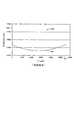
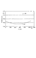
[0055]図4は、図2Bに示す「X」方向に移動される距離の関数として、石英基板108(図2Bによる)の上部表面に生成されるクロム線の平均CDを例示するグラフ400を示す。しかしながら、試験片を加工するために使用されるフォトレジストは、以前I線撮像に使用されたジアゾキノン増感されたノボラックベースのフォトレジストではなく、出願人の9−アントラセンメタノール増感剤が添加されたDX1100DUVフォトレジストである。特に、図4は、平均CDを軸402に示し、「X」方向に移動される距離を軸404に示す。曲線406に例示するように、CDのばらつきは、X=0μmにおける約1755nmからX=2700μmにおける約1746nm、更には、X=5400μmにおける約1755nmまで変動する。CDにおける差は、クロム線の全長にわたって約9nmだけである。
Claims (6)
- 集中及び分離した特徴を含む、フォトマスク加工、半導体装置の製造又は基板へのMEMS特徴の加工における光近接効果を減少する方法であって、
364nm〜436nmの範囲の波長を有する撮像放射線の使用を可能にしながら光近接効果を減少するようにDUVフォトレジストとともに機能する増感剤を前記DUVフォトレジストに添加するステップを備え、
前記増感剤が、前記DUVフォトレジスト中のベース樹脂と会合し、アントラセン発色団、ナフタレン発色団、或いはその組み合わせを備える、方法。 - 集中及び分離した特徴を含む、フォトマスク加工、半導体装置の製造又は基板へのMEMS特徴の加工における光近接効果を減少する方法であって、
364nm〜436nmの範囲の波長を有する撮像放射線の使用を可能にしながら光近接効果を減少するようにDUVフォトレジストとともに機能する増感剤を前記DUVフォトレジストに添加するステップを備え、
前記増感剤が、前記DUVフォトレジスト中の光化学増幅化合物と会合し、アントラセン発色団、ナフタレン発色団、或いはその組み合わせを備える、方法。 - 前記DUVフォトレジストが、置換ポリヒドロキシスチレン又はその共重合体を備える、請求項1又は2に記載の方法。
- 前記光化学増幅化合物が、オニウム塩メタルハライド複合体、トリフリック及びその派生物、トシレート及びその派生物、並びに、メシレート及びその派生物からなる群から選択される、請求項1又は2に記載の方法。
- 前記DUVフォトレジストが、オニウム塩メタルハライド複合体である光化学増幅化合物を備える、請求項4に記載の方法。
- 前記オニウム塩メタルハライド複合体がアリールスルホニウム塩である、請求項5に記載の方法。
Applications Claiming Priority (2)
| Application Number | Priority Date | Filing Date | Title |
|---|---|---|---|
| US10/155,523 US7067227B2 (en) | 2002-05-23 | 2002-05-23 | Sensitized chemically amplified photoresist for use in photomask fabrication and semiconductor processing |
| US10/155,523 | 2002-05-23 |
Related Parent Applications (1)
| Application Number | Title | Priority Date | Filing Date |
|---|---|---|---|
| JP2004515696A Division JP4427447B2 (ja) | 2002-05-23 | 2003-05-23 | フォトマスク加工及び半導体処理において使用する増感され化学的に増幅されたフォトレジスト |
Publications (2)
| Publication Number | Publication Date |
|---|---|
| JP2010092058A true JP2010092058A (ja) | 2010-04-22 |
| JP4996667B2 JP4996667B2 (ja) | 2012-08-08 |
Family
ID=29549089
Family Applications (2)
| Application Number | Title | Priority Date | Filing Date |
|---|---|---|---|
| JP2004515696A Expired - Fee Related JP4427447B2 (ja) | 2002-05-23 | 2003-05-23 | フォトマスク加工及び半導体処理において使用する増感され化学的に増幅されたフォトレジスト |
| JP2009249149A Expired - Fee Related JP4996667B2 (ja) | 2002-05-23 | 2009-10-29 | フォトマスク加工及び半導体処理において使用する増感され化学的に増幅されたフォトレジスト |
Family Applications Before (1)
| Application Number | Title | Priority Date | Filing Date |
|---|---|---|---|
| JP2004515696A Expired - Fee Related JP4427447B2 (ja) | 2002-05-23 | 2003-05-23 | フォトマスク加工及び半導体処理において使用する増感され化学的に増幅されたフォトレジスト |
Country Status (5)
| Country | Link |
|---|---|
| US (1) | US7067227B2 (ja) |
| EP (1) | EP1506454A2 (ja) |
| JP (2) | JP4427447B2 (ja) |
| KR (1) | KR20050010821A (ja) |
| WO (1) | WO2004001797A2 (ja) |
Families Citing this family (15)
| Publication number | Priority date | Publication date | Assignee | Title |
|---|---|---|---|---|
| US20050229145A1 (en) * | 2004-03-29 | 2005-10-13 | Irby John H Iv | Method and system for chrome cut-out regions on a reticle |
| US20050271711A1 (en) | 2004-04-26 | 2005-12-08 | The Procter & Gamble Company | Therapeutic antimicrobial compositions and methods |
| JP2006145853A (ja) * | 2004-11-19 | 2006-06-08 | Jsr Corp | 感放射線性樹脂組成物およびメッキ造形物の製造方法 |
| JP4828201B2 (ja) * | 2005-10-19 | 2011-11-30 | 東京応化工業株式会社 | 化学増幅型ホトレジスト組成物、レジスト層積層体およびレジストパタ−ン形成方法 |
| US7754394B2 (en) * | 2006-11-14 | 2010-07-13 | International Business Machines Corporation | Method to etch chrome for photomask fabrication |
| US7965382B2 (en) * | 2006-12-08 | 2011-06-21 | Applied Materials, Inc. | Methods and apparatus for multi-exposure patterning |
| US20080192253A1 (en) * | 2007-02-08 | 2008-08-14 | Susie Xiuru Yang | Method and test-structure for determining an offset between lithographic masks |
| US8292402B2 (en) * | 2008-02-13 | 2012-10-23 | Lexmark International, Inc. | Photoimageable dry film formulation |
| US9500948B2 (en) * | 2013-05-31 | 2016-11-22 | Orthogonal, Inc. | Fluorinated photoresist with integrated sensitizer |
| US20140356789A1 (en) * | 2013-05-31 | 2014-12-04 | Orthogonal, Inc. | Fluorinated photopolymer with integrated anthracene sensitizer |
| KR102254558B1 (ko) | 2013-11-13 | 2021-05-24 | 올싸거널 인코포레이티드 | 분지형 플루오르화 광중합체 |
| JP6344640B2 (ja) * | 2013-11-27 | 2018-06-20 | 川崎化成工業株式会社 | ラジカル重合増感剤 |
| WO2015120025A1 (en) | 2014-02-07 | 2015-08-13 | Orthogonal, Inc. | Cross-linkable fluorinated photopolymer |
| JP6537261B2 (ja) * | 2014-12-09 | 2019-07-03 | 旭有機材株式会社 | 樹脂原料、フェノール樹脂及びアントラセン誘導体の製造方法 |
| WO2016105473A1 (en) | 2014-12-24 | 2016-06-30 | Orthogonal, Inc. | Photolithographic patterning of electronic devices |
Citations (5)
| Publication number | Priority date | Publication date | Assignee | Title |
|---|---|---|---|---|
| JPH09304931A (ja) * | 1996-05-13 | 1997-11-28 | Toyo Ink Mfg Co Ltd | 感エネルギー線ポジ型感応性組成物 |
| JPH1026829A (ja) * | 1996-07-10 | 1998-01-27 | Japan Synthetic Rubber Co Ltd | 感放射線性樹脂組成物 |
| JPH11265061A (ja) * | 1998-01-15 | 1999-09-28 | Shipley Co Llc | 色素含有感光性耐食膜および方法ならびにこれを含む工業製品 |
| JP2000035665A (ja) * | 1998-05-11 | 2000-02-02 | Kunihiro Ichimura | 酸増殖剤及び感光性組成物 |
| WO2000008525A1 (en) * | 1998-08-07 | 2000-02-17 | Clariant International Ltd. | Radiation-sensitive composition of chemical amplification type |
Family Cites Families (22)
| Publication number | Priority date | Publication date | Assignee | Title |
|---|---|---|---|---|
| US5278010A (en) | 1989-03-03 | 1994-01-11 | International Business Machines Corporation | Composition for photo imaging |
| US5023164A (en) | 1989-10-23 | 1991-06-11 | International Business Machines Corporation | Highly sensitive dry developable deep UV photoresist |
| US5055439A (en) | 1989-12-27 | 1991-10-08 | International Business Machines Corporation | Photoacid generating composition and sensitizer therefor |
| KR930008139B1 (en) * | 1990-08-30 | 1993-08-26 | Samsung Electronics Co Ltd | Method for preparation of pattern |
| US5322765A (en) | 1991-11-22 | 1994-06-21 | International Business Machines Corporation | Dry developable photoresist compositions and method for use thereof |
| WO1994024610A1 (en) * | 1993-04-13 | 1994-10-27 | Astarix, Inc. | High resolution mask programmable via selected by low resolution photomasking |
| JPH07140666A (ja) * | 1993-06-04 | 1995-06-02 | Internatl Business Mach Corp <Ibm> | マイクロリトグラフィックレジスト組成物、酸不安定化合物、マイクロリトグラフィックレリーフ画像形成方法及び酸感知性ポリマー組成物 |
| KR960015081A (ko) * | 1993-07-15 | 1996-05-22 | 마쯔모또 에이이찌 | 화학증폭형 레지스트 조성물 |
| JP3203995B2 (ja) * | 1993-12-24 | 2001-09-04 | ジェイエスアール株式会社 | 感放射線性樹脂組成物 |
| EP0675410B1 (en) | 1994-03-28 | 1999-08-04 | Wako Pure Chemical Industries Ltd | Resist composition for deep ultraviolet light |
| JP3317576B2 (ja) * | 1994-05-12 | 2002-08-26 | 富士写真フイルム株式会社 | ポジ型感光性樹脂組成物 |
| JP3579946B2 (ja) | 1995-02-13 | 2004-10-20 | Jsr株式会社 | 化学増幅型感放射線性樹脂組成物 |
| US5609989A (en) * | 1995-06-06 | 1997-03-11 | International Business Machines, Corporation | Acid scavengers for use in chemically amplified photoresists |
| JP3433017B2 (ja) * | 1995-08-31 | 2003-08-04 | 株式会社東芝 | 感光性組成物 |
| ATE244904T1 (de) | 1995-12-21 | 2003-07-15 | Wako Pure Chem Ind Ltd | Polymerzusammensetzung und rezistmaterial |
| JP3589365B2 (ja) * | 1996-02-02 | 2004-11-17 | 富士写真フイルム株式会社 | ポジ画像形成組成物 |
| JP3808140B2 (ja) * | 1996-09-10 | 2006-08-09 | Azエレクトロニックマテリアルズ株式会社 | 新規酸感応性基で保護されたヒドロキシスチレン重合体およびこれらを含む放射線感応性材料 |
| US5955222A (en) * | 1996-12-03 | 1999-09-21 | International Business Machines Corporation | Method of making a rim-type phase-shift mask and mask manufactured thereby |
| US6103447A (en) * | 1998-02-25 | 2000-08-15 | International Business Machines Corp. | Approach to formulating irradiation sensitive positive resists |
| US6303263B1 (en) * | 1998-02-25 | 2001-10-16 | International Business Machines Machines | Irradiation sensitive positive-tone resists using polymers containing two acid sensitive protecting groups |
| US6210856B1 (en) * | 1999-01-27 | 2001-04-03 | International Business Machines Corporation | Resist composition and process of forming a patterned resist layer on a substrate |
| US6251564B1 (en) * | 1999-05-17 | 2001-06-26 | United Microelectronics Corp. | Method for forming a pattern with both logic-type and memory-type circuit |
-
2002
- 2002-05-23 US US10/155,523 patent/US7067227B2/en not_active Expired - Fee Related
-
2003
- 2003-05-23 WO PCT/US2003/016058 patent/WO2004001797A2/en not_active Ceased
- 2003-05-23 EP EP03748908A patent/EP1506454A2/en not_active Withdrawn
- 2003-05-23 JP JP2004515696A patent/JP4427447B2/ja not_active Expired - Fee Related
- 2003-05-23 KR KR10-2004-7018660A patent/KR20050010821A/ko not_active Ceased
-
2009
- 2009-10-29 JP JP2009249149A patent/JP4996667B2/ja not_active Expired - Fee Related
Patent Citations (5)
| Publication number | Priority date | Publication date | Assignee | Title |
|---|---|---|---|---|
| JPH09304931A (ja) * | 1996-05-13 | 1997-11-28 | Toyo Ink Mfg Co Ltd | 感エネルギー線ポジ型感応性組成物 |
| JPH1026829A (ja) * | 1996-07-10 | 1998-01-27 | Japan Synthetic Rubber Co Ltd | 感放射線性樹脂組成物 |
| JPH11265061A (ja) * | 1998-01-15 | 1999-09-28 | Shipley Co Llc | 色素含有感光性耐食膜および方法ならびにこれを含む工業製品 |
| JP2000035665A (ja) * | 1998-05-11 | 2000-02-02 | Kunihiro Ichimura | 酸増殖剤及び感光性組成物 |
| WO2000008525A1 (en) * | 1998-08-07 | 2000-02-17 | Clariant International Ltd. | Radiation-sensitive composition of chemical amplification type |
Also Published As
| Publication number | Publication date |
|---|---|
| EP1506454A2 (en) | 2005-02-16 |
| JP2005527003A (ja) | 2005-09-08 |
| US7067227B2 (en) | 2006-06-27 |
| US20030219675A1 (en) | 2003-11-27 |
| WO2004001797A3 (en) | 2004-07-01 |
| JP4996667B2 (ja) | 2012-08-08 |
| WO2004001797A9 (en) | 2004-02-12 |
| JP4427447B2 (ja) | 2010-03-10 |
| KR20050010821A (ko) | 2005-01-28 |
| WO2004001797A2 (en) | 2003-12-31 |
Similar Documents
| Publication | Publication Date | Title |
|---|---|---|
| JP4996667B2 (ja) | フォトマスク加工及び半導体処理において使用する増感され化学的に増幅されたフォトレジスト | |
| TWI380133B (en) | Hardmask composition having antireflective properties and method of patterning material on substrate using the same | |
| US6703169B2 (en) | Method of preparing optically imaged high performance photomasks | |
| US6727047B2 (en) | Method of extending the stability of a photoresist during direct writing of an image upon the photoresist | |
| TW522290B (en) | Organic bottom antireflective coating for high performance mask making using optical imaging | |
| US7244334B2 (en) | Apparatus used in reshaping a surface of a photoresist | |
| JPH08222508A (ja) | 感光性組成物のパターン形成方法 | |
| US6162565A (en) | Dilute acid rinse after develop for chrome etch | |
| US6969569B2 (en) | Method of extending the stability of a photoresist during direct writing of an image | |
| WO2002010858A2 (en) | Process for manufacturing a microelectronic device | |
| US12543542B2 (en) | Patterning method using secondary resist surface functionalization for mask formation | |
| US20050221019A1 (en) | Method of improving the uniformity of a patterned resist on a photomask | |
| US20070065756A1 (en) | High sensitivity electron beam resist processing | |
| JP2001318472A5 (ja) | ||
| JP4476492B2 (ja) | 電子線レジスト | |
| JPH0945651A (ja) | レジストの洗浄装置及び現像装置 | |
| CN114686057A (zh) | 一种图形化用抗反射涂层组合物及图形化方法 | |
| US20060105248A1 (en) | Method of reducing the average process bias during production of a reticle | |
| JP2011071170A (ja) | パターン形成方法及びパターン形成装置 |
Legal Events
| Date | Code | Title | Description |
|---|---|---|---|
| RD03 | Notification of appointment of power of attorney |
Free format text: JAPANESE INTERMEDIATE CODE: A7423 Effective date: 20101118 |
|
| RD04 | Notification of resignation of power of attorney |
Free format text: JAPANESE INTERMEDIATE CODE: A7424 Effective date: 20101209 |
|
| TRDD | Decision of grant or rejection written | ||
| A01 | Written decision to grant a patent or to grant a registration (utility model) |
Free format text: JAPANESE INTERMEDIATE CODE: A01 Effective date: 20120412 |
|
| A01 | Written decision to grant a patent or to grant a registration (utility model) |
Free format text: JAPANESE INTERMEDIATE CODE: A01 |
|
| A61 | First payment of annual fees (during grant procedure) |
Free format text: JAPANESE INTERMEDIATE CODE: A61 Effective date: 20120511 |
|
| FPAY | Renewal fee payment (event date is renewal date of database) |
Free format text: PAYMENT UNTIL: 20150518 Year of fee payment: 3 |
|
| R150 | Certificate of patent or registration of utility model |
Free format text: JAPANESE INTERMEDIATE CODE: R150 |
|
| R250 | Receipt of annual fees |
Free format text: JAPANESE INTERMEDIATE CODE: R250 |
|
| LAPS | Cancellation because of no payment of annual fees |