JP2010080658A - 膜形成用組成物、絶縁膜、半導体装置およびその製造方法 - Google Patents
膜形成用組成物、絶縁膜、半導体装置およびその製造方法 Download PDFInfo
- Publication number
- JP2010080658A JP2010080658A JP2008246845A JP2008246845A JP2010080658A JP 2010080658 A JP2010080658 A JP 2010080658A JP 2008246845 A JP2008246845 A JP 2008246845A JP 2008246845 A JP2008246845 A JP 2008246845A JP 2010080658 A JP2010080658 A JP 2010080658A
- Authority
- JP
- Japan
- Prior art keywords
- film
- silicon oxide
- organic silicon
- semiconductor device
- oxide film
- Prior art date
- Legal status (The legal status is an assumption and is not a legal conclusion. Google has not performed a legal analysis and makes no representation as to the accuracy of the status listed.)
- Granted
Links
- UYLSVYARXBFEKV-UHFFFAOYSA-O NC(C1)CC1[NH3+] Chemical compound NC(C1)CC1[NH3+] UYLSVYARXBFEKV-UHFFFAOYSA-O 0.000 description 1
- VHCQWQAYVBRQQC-UHFFFAOYSA-P [NH3+]C(CC1)C1[NH3+] Chemical compound [NH3+]C(CC1)C1[NH3+] VHCQWQAYVBRQQC-UHFFFAOYSA-P 0.000 description 1
Images










Classifications
-
- H—ELECTRICITY
- H10—SEMICONDUCTOR DEVICES; ELECTRIC SOLID-STATE DEVICES NOT OTHERWISE PROVIDED FOR
- H10W—GENERIC PACKAGES, INTERCONNECTIONS, CONNECTORS OR OTHER CONSTRUCTIONAL DETAILS OF DEVICES COVERED BY CLASS H10
- H10W20/00—Interconnections in chips, wafers or substrates
- H10W20/01—Manufacture or treatment
- H10W20/071—Manufacture or treatment of dielectric parts thereof
-
- C—CHEMISTRY; METALLURGY
- C07—ORGANIC CHEMISTRY
- C07F—ACYCLIC, CARBOCYCLIC OR HETEROCYCLIC COMPOUNDS CONTAINING ELEMENTS OTHER THAN CARBON, HYDROGEN, HALOGEN, OXYGEN, NITROGEN, SULFUR, SELENIUM OR TELLURIUM
- C07F7/00—Compounds containing elements of Groups 4 or 14 of the Periodic Table
- C07F7/02—Silicon compounds
- C07F7/08—Compounds having one or more C—Si linkages
- C07F7/18—Compounds having one or more C—Si linkages as well as one or more C—O—Si linkages
- C07F7/1804—Compounds having Si-O-C linkages
-
- H—ELECTRICITY
- H10—SEMICONDUCTOR DEVICES; ELECTRIC SOLID-STATE DEVICES NOT OTHERWISE PROVIDED FOR
- H10P—GENERIC PROCESSES OR APPARATUS FOR THE MANUFACTURE OR TREATMENT OF DEVICES COVERED BY CLASS H10
- H10P14/00—Formation of materials, e.g. in the shape of layers or pillars
- H10P14/60—Formation of materials, e.g. in the shape of layers or pillars of insulating materials
- H10P14/65—Formation of materials, e.g. in the shape of layers or pillars of insulating materials characterised by treatments performed before or after the formation of the materials
- H10P14/6516—Formation of materials, e.g. in the shape of layers or pillars of insulating materials characterised by treatments performed before or after the formation of the materials of treatments performed after formation of the materials
- H10P14/6529—Formation of materials, e.g. in the shape of layers or pillars of insulating materials characterised by treatments performed before or after the formation of the materials of treatments performed after formation of the materials by exposure to a gas or vapour
-
- H—ELECTRICITY
- H10—SEMICONDUCTOR DEVICES; ELECTRIC SOLID-STATE DEVICES NOT OTHERWISE PROVIDED FOR
- H10P—GENERIC PROCESSES OR APPARATUS FOR THE MANUFACTURE OR TREATMENT OF DEVICES COVERED BY CLASS H10
- H10P14/00—Formation of materials, e.g. in the shape of layers or pillars
- H10P14/60—Formation of materials, e.g. in the shape of layers or pillars of insulating materials
- H10P14/65—Formation of materials, e.g. in the shape of layers or pillars of insulating materials characterised by treatments performed before or after the formation of the materials
- H10P14/6516—Formation of materials, e.g. in the shape of layers or pillars of insulating materials characterised by treatments performed before or after the formation of the materials of treatments performed after formation of the materials
- H10P14/6536—Formation of materials, e.g. in the shape of layers or pillars of insulating materials characterised by treatments performed before or after the formation of the materials of treatments performed after formation of the materials by exposure to radiation, e.g. visible light
- H10P14/6538—Formation of materials, e.g. in the shape of layers or pillars of insulating materials characterised by treatments performed before or after the formation of the materials of treatments performed after formation of the materials by exposure to radiation, e.g. visible light by exposure to UV light
-
- H—ELECTRICITY
- H10—SEMICONDUCTOR DEVICES; ELECTRIC SOLID-STATE DEVICES NOT OTHERWISE PROVIDED FOR
- H10P—GENERIC PROCESSES OR APPARATUS FOR THE MANUFACTURE OR TREATMENT OF DEVICES COVERED BY CLASS H10
- H10P14/00—Formation of materials, e.g. in the shape of layers or pillars
- H10P14/60—Formation of materials, e.g. in the shape of layers or pillars of insulating materials
- H10P14/65—Formation of materials, e.g. in the shape of layers or pillars of insulating materials characterised by treatments performed before or after the formation of the materials
- H10P14/6516—Formation of materials, e.g. in the shape of layers or pillars of insulating materials characterised by treatments performed before or after the formation of the materials of treatments performed after formation of the materials
- H10P14/6536—Formation of materials, e.g. in the shape of layers or pillars of insulating materials characterised by treatments performed before or after the formation of the materials of treatments performed after formation of the materials by exposure to radiation, e.g. visible light
- H10P14/6539—Formation of materials, e.g. in the shape of layers or pillars of insulating materials characterised by treatments performed before or after the formation of the materials of treatments performed after formation of the materials by exposure to radiation, e.g. visible light by exposure to corpuscular radiation, e.g. exposure to electrons, alpha-particles, protons or ions
-
- H—ELECTRICITY
- H10—SEMICONDUCTOR DEVICES; ELECTRIC SOLID-STATE DEVICES NOT OTHERWISE PROVIDED FOR
- H10P—GENERIC PROCESSES OR APPARATUS FOR THE MANUFACTURE OR TREATMENT OF DEVICES COVERED BY CLASS H10
- H10P14/00—Formation of materials, e.g. in the shape of layers or pillars
- H10P14/60—Formation of materials, e.g. in the shape of layers or pillars of insulating materials
- H10P14/66—Formation of materials, e.g. in the shape of layers or pillars of insulating materials characterised by the type of materials
- H10P14/668—Formation of materials, e.g. in the shape of layers or pillars of insulating materials characterised by the type of materials the materials being characterised by the deposition precursor materials
- H10P14/6681—Formation of materials, e.g. in the shape of layers or pillars of insulating materials characterised by the type of materials the materials being characterised by the deposition precursor materials the precursor containing a compound comprising Si
- H10P14/6682—Formation of materials, e.g. in the shape of layers or pillars of insulating materials characterised by the type of materials the materials being characterised by the deposition precursor materials the precursor containing a compound comprising Si the compound being a silane, e.g. disilane, methylsilane or chlorosilane
-
- H—ELECTRICITY
- H10—SEMICONDUCTOR DEVICES; ELECTRIC SOLID-STATE DEVICES NOT OTHERWISE PROVIDED FOR
- H10P—GENERIC PROCESSES OR APPARATUS FOR THE MANUFACTURE OR TREATMENT OF DEVICES COVERED BY CLASS H10
- H10P72/00—Handling or holding of wafers, substrates or devices during manufacture or treatment thereof
- H10P72/04—Apparatus for manufacture or treatment
- H10P72/0431—Apparatus for thermal treatment
- H10P72/0434—Apparatus for thermal treatment mainly by convection
-
- H—ELECTRICITY
- H10—SEMICONDUCTOR DEVICES; ELECTRIC SOLID-STATE DEVICES NOT OTHERWISE PROVIDED FOR
- H10P—GENERIC PROCESSES OR APPARATUS FOR THE MANUFACTURE OR TREATMENT OF DEVICES COVERED BY CLASS H10
- H10P72/00—Handling or holding of wafers, substrates or devices during manufacture or treatment thereof
- H10P72/04—Apparatus for manufacture or treatment
- H10P72/0431—Apparatus for thermal treatment
- H10P72/0436—Apparatus for thermal treatment mainly by radiation
-
- H—ELECTRICITY
- H10—SEMICONDUCTOR DEVICES; ELECTRIC SOLID-STATE DEVICES NOT OTHERWISE PROVIDED FOR
- H10P—GENERIC PROCESSES OR APPARATUS FOR THE MANUFACTURE OR TREATMENT OF DEVICES COVERED BY CLASS H10
- H10P95/00—Generic processes or apparatus for manufacture or treatments not covered by the other groups of this subclass
-
- H—ELECTRICITY
- H10—SEMICONDUCTOR DEVICES; ELECTRIC SOLID-STATE DEVICES NOT OTHERWISE PROVIDED FOR
- H10P—GENERIC PROCESSES OR APPARATUS FOR THE MANUFACTURE OR TREATMENT OF DEVICES COVERED BY CLASS H10
- H10P14/00—Formation of materials, e.g. in the shape of layers or pillars
- H10P14/60—Formation of materials, e.g. in the shape of layers or pillars of insulating materials
- H10P14/63—Formation of materials, e.g. in the shape of layers or pillars of insulating materials characterised by the formation processes
- H10P14/6326—Deposition processes
- H10P14/6328—Deposition from the gas or vapour phase
- H10P14/6334—Deposition from the gas or vapour phase using decomposition or reaction of gaseous or vapour phase compounds, i.e. chemical vapour deposition
- H10P14/6336—Deposition from the gas or vapour phase using decomposition or reaction of gaseous or vapour phase compounds, i.e. chemical vapour deposition in the presence of a plasma [PECVD]
-
- H—ELECTRICITY
- H10—SEMICONDUCTOR DEVICES; ELECTRIC SOLID-STATE DEVICES NOT OTHERWISE PROVIDED FOR
- H10P—GENERIC PROCESSES OR APPARATUS FOR THE MANUFACTURE OR TREATMENT OF DEVICES COVERED BY CLASS H10
- H10P14/00—Formation of materials, e.g. in the shape of layers or pillars
- H10P14/60—Formation of materials, e.g. in the shape of layers or pillars of insulating materials
- H10P14/63—Formation of materials, e.g. in the shape of layers or pillars of insulating materials characterised by the formation processes
- H10P14/6326—Deposition processes
- H10P14/6342—Liquid deposition, e.g. spin-coating, sol-gel techniques or spray coating
-
- H—ELECTRICITY
- H10—SEMICONDUCTOR DEVICES; ELECTRIC SOLID-STATE DEVICES NOT OTHERWISE PROVIDED FOR
- H10P—GENERIC PROCESSES OR APPARATUS FOR THE MANUFACTURE OR TREATMENT OF DEVICES COVERED BY CLASS H10
- H10P14/00—Formation of materials, e.g. in the shape of layers or pillars
- H10P14/60—Formation of materials, e.g. in the shape of layers or pillars of insulating materials
- H10P14/66—Formation of materials, e.g. in the shape of layers or pillars of insulating materials characterised by the type of materials
- H10P14/668—Formation of materials, e.g. in the shape of layers or pillars of insulating materials characterised by the type of materials the materials being characterised by the deposition precursor materials
- H10P14/6681—Formation of materials, e.g. in the shape of layers or pillars of insulating materials characterised by the type of materials the materials being characterised by the deposition precursor materials the precursor containing a compound comprising Si
- H10P14/6684—Formation of materials, e.g. in the shape of layers or pillars of insulating materials characterised by the type of materials the materials being characterised by the deposition precursor materials the precursor containing a compound comprising Si the compound comprising silicon and oxygen
- H10P14/6686—Formation of materials, e.g. in the shape of layers or pillars of insulating materials characterised by the type of materials the materials being characterised by the deposition precursor materials the precursor containing a compound comprising Si the compound comprising silicon and oxygen the compound being a molecule comprising at least one silicon-oxygen bond and the compound having hydrogen or an organic group attached to the silicon or oxygen, e.g. a siloxane
-
- H—ELECTRICITY
- H10—SEMICONDUCTOR DEVICES; ELECTRIC SOLID-STATE DEVICES NOT OTHERWISE PROVIDED FOR
- H10P—GENERIC PROCESSES OR APPARATUS FOR THE MANUFACTURE OR TREATMENT OF DEVICES COVERED BY CLASS H10
- H10P14/00—Formation of materials, e.g. in the shape of layers or pillars
- H10P14/60—Formation of materials, e.g. in the shape of layers or pillars of insulating materials
- H10P14/69—Inorganic materials
- H10P14/692—Inorganic materials composed of oxides, glassy oxides or oxide-based glasses
- H10P14/6921—Inorganic materials composed of oxides, glassy oxides or oxide-based glasses containing silicon
- H10P14/69215—Inorganic materials composed of oxides, glassy oxides or oxide-based glasses containing silicon the material being a silicon oxide, e.g. SiO2
-
- H—ELECTRICITY
- H10—SEMICONDUCTOR DEVICES; ELECTRIC SOLID-STATE DEVICES NOT OTHERWISE PROVIDED FOR
- H10P—GENERIC PROCESSES OR APPARATUS FOR THE MANUFACTURE OR TREATMENT OF DEVICES COVERED BY CLASS H10
- H10P14/00—Formation of materials, e.g. in the shape of layers or pillars
- H10P14/60—Formation of materials, e.g. in the shape of layers or pillars of insulating materials
- H10P14/69—Inorganic materials
- H10P14/692—Inorganic materials composed of oxides, glassy oxides or oxide-based glasses
- H10P14/6921—Inorganic materials composed of oxides, glassy oxides or oxide-based glasses containing silicon
- H10P14/6922—Inorganic materials composed of oxides, glassy oxides or oxide-based glasses containing silicon the material containing Si, O and at least one of H, N, C, F or other non-metal elements, e.g. SiOC, SiOC:H or SiONC
Landscapes
- Chemical & Material Sciences (AREA)
- Organic Chemistry (AREA)
- Formation Of Insulating Films (AREA)
- Silicon Polymers (AREA)
Abstract
【解決手段】本発明の一の態様によれば、下記一般式(I)で表される化合物またはその加水分解脱水縮合物を含むことを特徴とする、膜形成用組成物が提供される。
X1 3−mR1 mSiR2SiR3 nX2 3−n (I)
(式中、R1およびR3は水素原子または1価の置換基であり、R2は炭素数4の脂環構造を含む2価の基あるいはその誘導体であり、X1およびX2は加水分解性基であり、mおよびnは0〜2の整数である。)
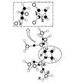
【選択図】図2
Description
X1 3−mR1 mSiR2SiR3 nX2 3−n (I)
(式中、R1およびR3は水素原子または1価の置換基であり、R2は炭素数4の脂環構造を含む2価の基あるいはその誘導体であり、X1およびX2は加水分解性基であり、mおよびnは0〜2の整数であり、R2の2価の基は、シクロブタン、シクロフロロブタン(−C4H6−XFX−)、シクロポリメチルブタン(−C4H6−X(CH3)X−)、シクロポリメチルフロロブタン(−C4H6−Y−Z(FY(CH3)Z)−)、シクロクロロブタン(−C4H6−XClX−)、シクロポリメチルクロロブタン(−C4H6−Y−Z(ClY(CH3)Z)−)である(式中、Xは1〜6の整数であり、YおよびZは1〜5の整数であり、かつ2≦Y+Z≦6の関係を満たす)。
以下、本発明の第1の実施の形態について説明する。本実施の形態の膜形成用組成物は、下記一般式(I)で表されるシラン化合物またはその加水分解脱水縮合物を含む。
式中、R1およびR3は水素原子または1価の置換基であり、非加水分解性基である。R1およびR3は、水素原子、アルキル基またはアリール基が好ましく、水素原子、メチル基またはフェニル基がより好ましく、メチル基が最も好ましい。
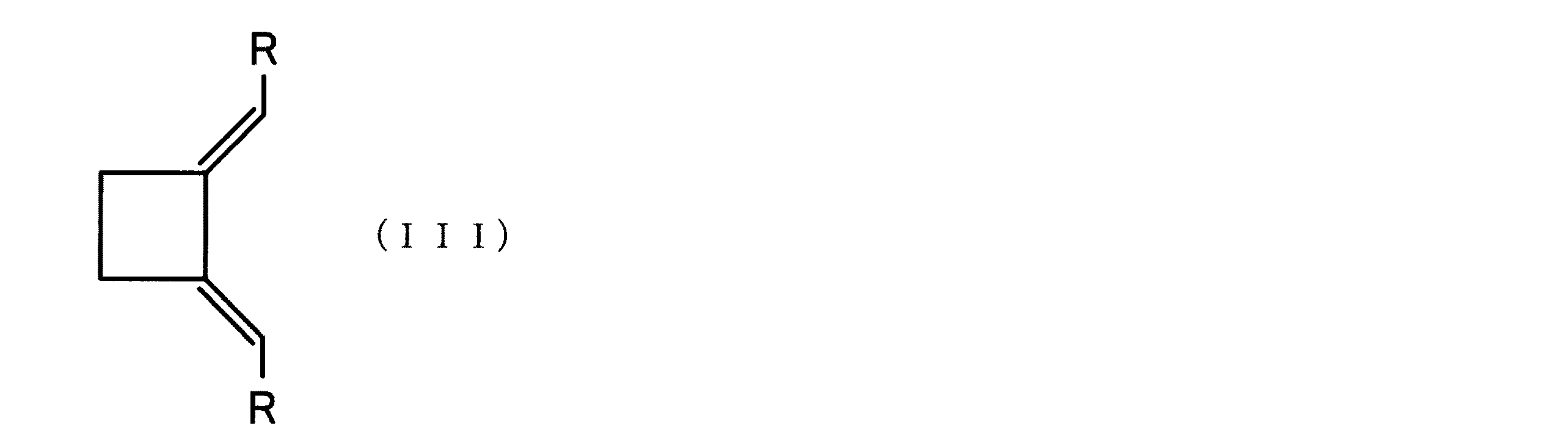
式中、R4は水素原子または置換基であり、非加水分解性基であるが、メチル基、フェニル基またはシクロアルキル基が好ましい。
上記の中でも、好ましい溶媒としてはプロピレングリコールモノメチルエーテルアセテート、プロピレングリコールモノメチルエーテル、2−ヘプタノン、シクロヘキサノン、γ−ブチロラクトン、エチレングリコールモノメチルエーテル、エチレングリコールモノエチルエーテル、エチレングリコールモノエチルエーテルアセテート、プロピレングリコールモノメチルエーテル、プロピレングリコールモノエチルエーテル、エチレンカーボネート、酢酸ブチル、乳酸メチル、乳酸エチル、メトキシプロピオン酸メチル、エトキシプロピオン酸エチル、N−メチルピロリドン、N,N−ジメチルホルムアミド、テトラヒドロフラン、メチルイソブチルケトン、キシレン、メシチレン、ジイソプロピルベンゼンを挙げることができる。
塗布法により膜を形成するには、まず、膜形成用組成物を上記溶媒で希釈して、シリコンウエハ等の基材上に塗布する。塗布手段としては、スピンコート、浸漬法、ロールコート法、スプレー法などが用いられる。この際の膜厚は、乾燥後の膜厚として、1回塗りで厚さ0.05〜1.5μm程度、2回塗りでは厚さ0.1〜3μm程度の塗膜を形成することができる。その後、常温で残留溶媒を揮発乾燥するか、ホットプレート、オーブン、ファーネスなどを使用して加熱することによって、残留溶媒の乾燥と架橋反応を進行させることにより、ガラス質または巨大高分子、またはその混合物の膜を形成することができる。
CVD法により膜を形成するには、まず、膜形成用組成物を上記溶媒で希釈安定化させることにより液体原料として準備する。この液体原料を加熱蒸発あるいは担体ガスによるバブリング蒸発等によりCVD原料ガスとして供給し、他の非酸化性希釈ガスや酸化性ガスとともに膜形成用組成物を基材上に供給し堆積させることにより、ガラス質または巨大高分子、またはその混合物である所望の低誘電率絶縁膜を形成することができる。
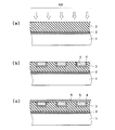
以下、本発明の第2の実施の形態について図面を参照しながら説明する。本実施の形態では、第1の実施の形態で説明した膜形成用組成物を用いて半導体装置の層間絶縁膜を形成した例について説明する。図14(a)〜図14(c)は第2の実施の形態に係る半導体装置の模式的な製造工程図である。
まず、スピンコート法にてワニスを半導体基板1上に塗布する。詳細には、半導体基板1上の下地絶縁膜2の表面上に、溶媒に膜材料の前駆体としてのシクロブタン架橋組成物を溶解させたワニスと呼ばれる液状原料を、コーターを用いてスピンコート法により塗布し、塗布膜を形成する。溶媒としては、例えばPGPE(プロピレングリコールモノプロピルエーテル)を用いることができる。
半導体基板1上に塗布膜を形成した後、半導体基板1に80℃で1分間熱処理を施す。詳細には、電子線照射処理を行う反応容器内に設置され、かつ80℃に保持されているホットプレート上に、塗布膜が形成された半導体基板1を載置する。この状態を1分間保持することにより、80℃、1分間の熱処理が上記塗布膜に施される。これにより塗布膜中の溶媒が除去される。
上記熱処理を施した後、半導体基板1に200℃以上350℃以下で1分間熱処理を施す。詳細には、上記ホットプレート上に、半導体基板1を載置したまま、ホットプレートの温度を200℃に保持する。この状態を1分間保持することにより、電子線照射処理を行う反応容器内で、200℃、1分間の熱処理が上記塗布膜に施される。これにより塗布膜中の化合物が架橋するとともに塗布膜が半導体基板1上に固定される。この工程は、酸化されやすい金属配線が露出していない限り、酸化性雰囲気であることが好ましい。
熱処理を施した後、減圧された雰囲気中で、半導体基板1を400℃以上600℃以下で加熱しつつ、電子線照射処理を行い、層間絶縁膜3を形成する。詳細には、反応容器内に窒素約20slmを導入し、減圧された窒素雰囲気中で半導体基板1を400℃に保持されたホットプレート上に載置した状態で、上記塗布膜に電子線を照射し、層間絶縁膜3を形成する。電子線が塗布膜に照射されると、塗布膜中の酸素分子、水分子、およびヒドロキシル基の結合が切断され、これにより生成された酸素原子で塗布膜が自動的かつ適度に酸化される。この工程は上記塗布膜の過剰な酸化を抑制するため、非酸化性雰囲気であることが好ましい。
以下、本発明の第3の実施の形態について図面を参照しながら説明する。本実施の形態では、第1の実施の形態で説明した膜形成用組成物を用いて半導体装置の層間絶縁膜を形成する際の電子線照射方法について説明する。本実施の形態は、第2の実施の形態で用いた電子線照射方法とは異なる電子線照射工程に特徴がある。そこで、本実施の形態の説明に先立ち、まず本実施の形態で用いた電子線照射装置について説明する。図15(a)および(b)は第3の実施の形態で用いる電子線照射装置の概略構成図である。
まず、膜材料の前駆体としての上記第1の実施の形態で説明したシクロブタン架橋組成物を溶解させたワニスを、シリコン窒化膜15の表面上に供給する。ワニスを供給する方法としては、本実施の形態においては、良質なシクロブタン架橋有機シリコン酸化膜が成膜されるように、ワニスを略均一な厚さでむらなく供給することができる塗布法を採用する。このワニスの塗布作業は、具体的には、塗布装置として、例えば図示しないコーターを用いて、塗布法の一種であるスピンコート法によってワニスをシリコン窒化膜15の表面上に塗布するものである。
第1層半導体基板16を、図16(c)に示されるように、そのワニスが塗布されたシリコン窒化膜5を上向きにした状態で、温度調節装置としてのホットプレート25(加熱装置)上に載置する。その後、ワニスの温度が約80℃に保持されるようにホットプレート25の温度を調節して、ワニスを第1層半導体基板16ごと加熱するとともに、この状態を約1分間保持する。これによりワニスに1回目の熱処理を施す。
第1層半導体基板16をホットプレート25上に載置した状態のまま、ワニスの温度が200℃に保持されるようにホットプレート25の温度を調節して、ワニスを第1層半導体基板16ごと加熱するとともに、この状態を約1分間保持する。これによりワニスに2回目の熱処理を施す。上記工程2および3の熱処理によって、ワニスに含まれる溶媒は蒸発によって除去され、シリコン窒化膜15上にワニス(塗布膜)は固定(固着)される。
第1層半導体基板16をホットプレート25上に載置した状態のまま、ワニスおよびこのワニスを基に成膜されるシクロブタン架橋有機シリコン酸化膜が酸化されないように、約1.3×10³Pa(10Torr)まで減圧した減圧雰囲気下に配置する。それとともに、第1層半導体基板16が配置される雰囲気を、還元性を有するH2ガスを主成分とするガスで満たす。上記H2ガスは、後述する電子線照射作業を行うときに、Cu配線14の表面をクリーニングし、該表面の酸化を抑制する。
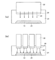
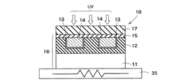
以下、本発明の第4の実施の形態について図面を参照しながら説明する。本実施の形態では、第1の実施の形態で説明した膜形成用組成物を用いて層間絶縁膜を形成する際の紫外線照射方法について説明する。そこで、本実施の形態の説明に先立ち、まず本実施の形態で用いた紫外線照射装置について説明する。図17(a)および(b)は第4の実施の形態で用いる紫外線照射装置の概略構成図である。なお、第3の実施の形態と重複する記載は、省略するものとする。
以下、本発明の第5の実施の形態について図面を参照しながら説明する。本実施の形態では、プラズマアシスト化学的気相成長法(プラズマCVD法)を用いてシクロブタン架橋有機シリコン酸化膜を形成した例について説明する。
以下、本発明の第6の実施の形態について図面を参照しながら説明する。本実施の形態では、第5の実施の形態とは異なるプラズマCVD法を用いてシクロブタン架橋有機シリコン酸化膜を形成した例について説明する。
シクロブタン架橋組成物
下記式(A)の1,2−ビス(トリエトキシシリル)アセチレンに対し、1.2モル当量のジルコノセンジエチルを混合し室温で1時間攪拌し、次いで1.2モル当量のヨウ素を混合し0℃で2時間攪拌し、最後に1.2モル当量の塩化銅(I)を混合し室温で6時間攪拌し順次反応させた。次いで、反応液をろ過して塩を除いた後、減圧濃縮し、アルミナカラムで精製して置換位置異性体の混合物として、1,2−ビス(トリエトキシシリル)シクロブテンを収率6割で得る。塩化銅(I)を反応させる際は、0.1モル当量を混合し室温で24時間攪拌した場合、あるいは50℃で6時間攪拌した場合においても、同等の収率でビス(トリエトキシシリル)シクロブテンを得た。引き続き、水素付加反応を行い、1,2−ビス(トリエトキシシリル)シクロブタン(I−1)を得る。
下記式(B)のビス(モノメチル・ジメトキシ)シロキサンエタンをプロピレングリコールモノプロピルエーテル7mlに溶解させ、0.4%硝酸水溶液200mgを加えて、12時間攪拌した後、液質量が6gになるまで減圧濃縮し、比較用組成物であるエチレン架橋組成物(B―1)を得る。
シクロブタン架橋組成物(I−1)および/またはエチレン架橋組成物(B−1)をプロピレングリコールモノエチルエーテルに溶解して薬液を調整する。得られた薬液をスピンコート法で300mmシリコンウエハ上に塗布後、ホットプレート上において80℃で1分間、200℃で1分間、基板を乾燥し、さらに酸素濃度500ppm以下の乾燥窒素雰囲気のクリーンオーブン中で380℃で20分間加熱することにより、有機シリコン酸化膜を作製する。
上記により作製された有機シリコン酸化膜の比誘電率、ヤング率、クラック耐性、およびO2プラズマ処理耐性を評価する。比誘電率は、MISキャパシタを作成し、膜厚と容量−電圧特性とを測定し決定することができる。またヤング率(膜強度)は、MTSシステムズ社製Nano Indenter XPで測定することができる。測定に必要な膜厚は最低で300nm必要である。これ以上薄い場合、Si基板の影響を受けるので正確な値は求められないおそれがある。
表2に比誘電率とヤング率の値を示す。
Claims (14)
- 下記一般式(I)で表される化合物またはその加水分解脱水縮合物を含むことを特徴とする、膜形成用組成物。
X1 3−mR1 mSiR2SiR3 nX2 3−n (I)
(式中、R1およびR3は水素原子または1価の置換基であり、R2は炭素数4の脂環構造を含む2価の基あるいはその誘導体であり、X1およびX2は加水分解性基であり、mおよびnは0〜2の整数である。) - 前記一般式(I)におけるR2の2価の基が、シクロブタン(−C4H6−)、シクロフロロブタン(−C4H6−XFX−)、シクロポリメチルブタン(−C4H6−X(CH3)X−)、シクロポリメチルフロロブタン(−C4H6−Y−Z(FY(CH3)Z)−)、シクロクロロブタン(−C4H6−XClX−)、シクロポリメチルクロロブタン(−C4H6−Y−Z(ClY(CH3)Z)−)である(式中、Xは1〜6の整数であり、YおよびZは1〜5の整数であり、かつ2≦Y+Z≦6の関係を満たす)、請求項1に記載の膜形成用組成物。
- 前記一般式(I)におけるR2の2価の基が、炭素数4の脂環構造(−C4X6−)骨格を有し、Xがオルト位置またはパラ位置にありかつトランスまたはゴーシュ(gauche)位置に結合している、請求項2に記載の膜形成用組成物。
- 前記一般式(I)におけるmおよびnが、m+n≧1を満たしている、請求項1〜3のいずれか1項に記載の膜形成用組成物。
- 前記一般式(I)におけるmおよびnが1である、請求項4に記載の膜形成用組成物。
- 下記一般式(II)で表される化合物またはその加水分解脱水縮合物をさらに含む、請求項1ないし5のいずれか1項に記載の膜形成用組成物。
R4 pSiX3 4−p (II)
(式中、R4は水素原子または置換基であり、X3は加水分解性基であり、pは0〜3の整数である。) - 請求項1ないし6のいずれかに1項に記載の膜形成用組成物を用いて製造された単独組成または混合組成の有機シリコン酸化膜からなることを特徴とする、絶縁膜。
- 前記一般式(I)における架橋基R2の個数とSiの個数の比であるR2/Siが、0.5以上2以下である、請求項7に記載の絶縁膜。
- 請求項7または8に記載の前記有機シリコン酸化膜を備えることを特徴とする、半導体装置。
- 請求項7または8に記載の前記有機シリコン酸化膜を備えた半導体装置の製造方法であって、
前記有機シリコン酸化膜の形成は、
請求項1ないし6のいずれか1項に記載の膜形成用組成物を用いて、塗布法またはプラズマ化学的気相成長法により膜を形成する工程と、
形成された前記膜に酸化性雰囲気で熱処理を施す工程と、
前記熱処理が施された膜に非酸化性雰囲気で熱処理を施す工程と
を含む工程により行われることを特徴とする、半導体装置の製造方法。 - 前記酸化性雰囲気での熱処理が200℃以上350℃以下で行われ、かつ前記非酸化性雰囲気での熱処理が400℃以上600℃以下で行われる、請求項10に記載の半導体装置。
- 請求項7または8に記載の前記有機シリコン酸化膜を備えた半導体装置の製造方法であって、
前記有機シリコン酸化膜の形成は、
請求項1ないし6のいずれか1項に記載の膜形成用組成物を用いて、塗布法またはプラズマ化学的気相成長法により膜を形成する工程と、
形成された前記膜に、減圧下において熱処理を施しつつエネルギー線を照射する工程と
を含む工程により行われることを特徴とする、半導体装置の製造方法。 - 前記熱処理が、0Pa以上5.5×10⁴Pa以下の圧力下で、200℃以上500℃以下で行われる、請求項12に記載の半導体装置の製造方法。
- 前記エネルギー線が、電子線あるいは紫外線である、請求項12または13に記載の半導体装置の製造方法。
Priority Applications (2)
| Application Number | Priority Date | Filing Date | Title |
|---|---|---|---|
| JP2008246845A JP5172567B2 (ja) | 2008-09-25 | 2008-09-25 | 膜形成用組成物、絶縁膜、半導体装置およびその製造方法 |
| US12/548,492 US7999356B2 (en) | 2008-09-25 | 2009-08-27 | Composition for film formation, insulating film, semiconductor device, and process for producing the semiconductor device |
Applications Claiming Priority (1)
| Application Number | Priority Date | Filing Date | Title |
|---|---|---|---|
| JP2008246845A JP5172567B2 (ja) | 2008-09-25 | 2008-09-25 | 膜形成用組成物、絶縁膜、半導体装置およびその製造方法 |
Publications (2)
| Publication Number | Publication Date |
|---|---|
| JP2010080658A true JP2010080658A (ja) | 2010-04-08 |
| JP5172567B2 JP5172567B2 (ja) | 2013-03-27 |
Family
ID=42036775
Family Applications (1)
| Application Number | Title | Priority Date | Filing Date |
|---|---|---|---|
| JP2008246845A Expired - Fee Related JP5172567B2 (ja) | 2008-09-25 | 2008-09-25 | 膜形成用組成物、絶縁膜、半導体装置およびその製造方法 |
Country Status (2)
| Country | Link |
|---|---|
| US (1) | US7999356B2 (ja) |
| JP (1) | JP5172567B2 (ja) |
Cited By (1)
| Publication number | Priority date | Publication date | Assignee | Title |
|---|---|---|---|---|
| JP2021507031A (ja) * | 2017-12-19 | 2021-02-22 | ハネウェル・インターナショナル・インコーポレーテッドHoneywell International Inc. | 耐亀裂性ケイ素系平坦化組成物、方法、及びフィルム |
Families Citing this family (14)
| Publication number | Priority date | Publication date | Assignee | Title |
|---|---|---|---|---|
| US9257302B1 (en) | 2004-03-25 | 2016-02-09 | Novellus Systems, Inc. | CVD flowable gap fill |
| US9245739B2 (en) * | 2006-11-01 | 2016-01-26 | Lam Research Corporation | Low-K oxide deposition by hydrolysis and condensation |
| US8220136B2 (en) * | 2007-05-03 | 2012-07-17 | Hitachi Global Storage Technologies Netherlands B. V. | Forming a planarized surface for at least one bar of sliders |
| US9719169B2 (en) | 2010-12-20 | 2017-08-01 | Novellus Systems, Inc. | System and apparatus for flowable deposition in semiconductor fabrication |
| JP5889118B2 (ja) | 2012-06-13 | 2016-03-22 | 株式会社東芝 | 半導体装置及びその製造方法 |
| US9305880B2 (en) * | 2013-10-24 | 2016-04-05 | Taiwan Semiconductor Manufacturing Co., Ltd. | Interconnects for semiconductor devices |
| US9847222B2 (en) | 2013-10-25 | 2017-12-19 | Lam Research Corporation | Treatment for flowable dielectric deposition on substrate surfaces |
| US10049921B2 (en) | 2014-08-20 | 2018-08-14 | Lam Research Corporation | Method for selectively sealing ultra low-k porous dielectric layer using flowable dielectric film formed from vapor phase dielectric precursor |
| US9502255B2 (en) | 2014-10-17 | 2016-11-22 | Lam Research Corporation | Low-k damage repair and pore sealing agents with photosensitive end groups |
| CN104282250B (zh) * | 2014-10-24 | 2016-08-31 | 深圳市华星光电技术有限公司 | Tft 中mis 结构设计的控制方法及系统 |
| US9916977B2 (en) | 2015-11-16 | 2018-03-13 | Lam Research Corporation | Low k dielectric deposition via UV driven photopolymerization |
| US10388546B2 (en) | 2015-11-16 | 2019-08-20 | Lam Research Corporation | Apparatus for UV flowable dielectric |
| WO2018195454A1 (en) | 2017-04-20 | 2018-10-25 | De Rochemont L Pierre | Resonant high energy density storage device |
| JP7009111B2 (ja) * | 2017-08-17 | 2022-01-25 | キヤノン株式会社 | 半導体装置及びその製造方法 |
Citations (5)
| Publication number | Priority date | Publication date | Assignee | Title |
|---|---|---|---|---|
| JP2006216541A (ja) * | 2005-01-21 | 2006-08-17 | Internatl Business Mach Corp <Ibm> | 誘電体材料、相互接続構造、電子構造、電子センシング構造および該製作方法(改良された靭性および改良されたSi−C結合を有するSiCOH誘電体材料、該誘電体材料を含む半導体デバイスおよび該誘電体材料の製作方法) |
| WO2006088015A1 (ja) * | 2005-02-18 | 2006-08-24 | Nec Corporation | 有機シリコン系膜の形成方法、当該有機シリコン系膜を有する半導体装置及びその製造方法 |
| JP2006241304A (ja) * | 2005-03-03 | 2006-09-14 | Fuji Photo Film Co Ltd | 膜形成用組成物、絶縁膜およびその製造方法 |
| JP2007016177A (ja) * | 2005-07-08 | 2007-01-25 | Fujitsu Ltd | シリカ系被膜形成用材料、シリカ系被膜及びその製造方法、多層配線及びその製造方法、並びに、半導体装置及びその製造方法 |
| JP2008010877A (ja) * | 2006-06-27 | 2008-01-17 | Air Products & Chemicals Inc | 還元性雰囲気下における絶縁膜の硬化 |
Family Cites Families (9)
| Publication number | Priority date | Publication date | Assignee | Title |
|---|---|---|---|---|
| JPH11186996A (ja) | 1997-12-18 | 1999-07-09 | Oki Tec:Kk | 位相乗り換え回路 |
| JP2001098183A (ja) | 1999-09-29 | 2001-04-10 | Sumitomo Chem Co Ltd | 反応染料組成物及びそれを用いる繊維材料の染色方法 |
| JP2001096678A (ja) | 1999-10-01 | 2001-04-10 | Toko Shizai Kogyo Kk | 熱収縮フィルム及びその製造方法 |
| JP2001140275A (ja) | 1999-11-12 | 2001-05-22 | Hitachi Constr Mach Co Ltd | 側溝掘用建設機械 |
| JP3718709B2 (ja) | 2000-07-28 | 2005-11-24 | 国立大学法人東北大学 | 新規なシクロブタン誘導体及びその合成方法 |
| JP3530165B2 (ja) | 2000-10-20 | 2004-05-24 | 株式会社東芝 | 半導体装置の製造方法 |
| JP3987944B2 (ja) | 2004-07-22 | 2007-10-10 | 国立大学法人東北大学 | 多置換シクロブタン及び多置換シクロブテン化合物の製造方法 |
| JP2006111738A (ja) | 2004-10-15 | 2006-04-27 | Jsr Corp | 表面疎水化用組成物、表面疎水化方法、半導体装置およびその製造方法 |
| JP4437071B2 (ja) | 2004-12-24 | 2010-03-24 | パナソニック株式会社 | 運転支援装置 |
-
2008
- 2008-09-25 JP JP2008246845A patent/JP5172567B2/ja not_active Expired - Fee Related
-
2009
- 2009-08-27 US US12/548,492 patent/US7999356B2/en active Active
Patent Citations (5)
| Publication number | Priority date | Publication date | Assignee | Title |
|---|---|---|---|---|
| JP2006216541A (ja) * | 2005-01-21 | 2006-08-17 | Internatl Business Mach Corp <Ibm> | 誘電体材料、相互接続構造、電子構造、電子センシング構造および該製作方法(改良された靭性および改良されたSi−C結合を有するSiCOH誘電体材料、該誘電体材料を含む半導体デバイスおよび該誘電体材料の製作方法) |
| WO2006088015A1 (ja) * | 2005-02-18 | 2006-08-24 | Nec Corporation | 有機シリコン系膜の形成方法、当該有機シリコン系膜を有する半導体装置及びその製造方法 |
| JP2006241304A (ja) * | 2005-03-03 | 2006-09-14 | Fuji Photo Film Co Ltd | 膜形成用組成物、絶縁膜およびその製造方法 |
| JP2007016177A (ja) * | 2005-07-08 | 2007-01-25 | Fujitsu Ltd | シリカ系被膜形成用材料、シリカ系被膜及びその製造方法、多層配線及びその製造方法、並びに、半導体装置及びその製造方法 |
| JP2008010877A (ja) * | 2006-06-27 | 2008-01-17 | Air Products & Chemicals Inc | 還元性雰囲気下における絶縁膜の硬化 |
Cited By (4)
| Publication number | Priority date | Publication date | Assignee | Title |
|---|---|---|---|---|
| JP2021507031A (ja) * | 2017-12-19 | 2021-02-22 | ハネウェル・インターナショナル・インコーポレーテッドHoneywell International Inc. | 耐亀裂性ケイ素系平坦化組成物、方法、及びフィルム |
| JP7374092B2 (ja) | 2017-12-19 | 2023-11-06 | ハネウェル・インターナショナル・インコーポレーテッド | 耐亀裂性ケイ素系平坦化組成物、方法、及びフィルム |
| KR20240058957A (ko) * | 2017-12-19 | 2024-05-03 | 허니웰 인터내셔날 인코포레이티드 | 내균열성 규소계 평탄화 조성물, 방법 및 필름 |
| KR102817158B1 (ko) | 2017-12-19 | 2025-06-05 | 허니웰 인터내셔날 인코포레이티드 | 내균열성 규소계 평탄화 조성물, 방법 및 필름 |
Also Published As
| Publication number | Publication date |
|---|---|
| JP5172567B2 (ja) | 2013-03-27 |
| US20100072581A1 (en) | 2010-03-25 |
| US7999356B2 (en) | 2011-08-16 |
Similar Documents
| Publication | Publication Date | Title |
|---|---|---|
| JP5172567B2 (ja) | 膜形成用組成物、絶縁膜、半導体装置およびその製造方法 | |
| JP4374567B2 (ja) | 多孔性低誘電率材料のための紫外線硬化処理 | |
| CN100361280C (zh) | 多孔低介电常数材料的等离子固化方法 | |
| JP5592327B2 (ja) | 誘電体膜の材料特性を高めるための活性化学的方法 | |
| JP4434146B2 (ja) | 多孔質絶縁膜及びその製造方法並びに多孔質絶縁膜を用いた半導体装置 | |
| TWI431040B (zh) | Organic silicon dioxide film and method for forming the same, composition for forming insulating film of semiconductor device and manufacturing method thereof, and wiring structure | |
| US20070299239A1 (en) | Curing Dielectric Films Under A Reducing Atmosphere | |
| JP5160237B2 (ja) | 低誘電率非晶質シリカ系被膜形成用塗布液および該塗布液から得られる低誘電率非晶質シリカ系被膜 | |
| CN101060095A (zh) | 形成受控的空隙的材料和方法 | |
| EP1296365B1 (en) | Method of film formation | |
| CN103276370A (zh) | 多孔低介电常数组合物、其制备方法及其使用方法 | |
| JP5030478B2 (ja) | 多孔質膜の前駆体組成物及びその調製方法、多孔質膜及びその作製方法、並びに半導体装置 | |
| TW200536621A (en) | Method for producing polymer, polymer, composition for forming insulating film, method for producing insulating film, and insulating film | |
| TW202012419A (zh) | 矽化合物及使用其沉積膜的方法 | |
| JP4756128B2 (ja) | 半導体加工用保護膜形成用塗布液、その調製方法およびこれより得られる半導体加工用保護膜 | |
| TW200529252A (en) | Insulating film, method for forming same and composition for forming film | |
| WO2005108469A1 (ja) | 有機シリカ系膜の形成方法、有機シリカ系膜、配線構造体、半導体装置、および膜形成用組成物 | |
| WO2006025500A1 (ja) | 半導体装置の製造方法およびこれを用いて形成された半導体装置 | |
| US8431464B2 (en) | Process for producing silicic coating, silicic coating and semiconductor device | |
| US6749944B2 (en) | Stacked film, method for the formation of stacked film, insulating film, and substrate for semiconductor | |
| KR102409869B1 (ko) | 규소 화합물 및 이를 사용하여 막을 증착시키는 방법 | |
| TW202110862A (zh) | 單烷氧基矽烷及使用其製造的密有機二氧化矽膜 | |
| JP4422643B2 (ja) | 多孔質フィルムの製造方法ならびに層間絶縁膜、半導体材料および半導体装置 | |
| JP4150922B2 (ja) | 積層体の形成方法 | |
| JP2004356582A (ja) | 積層体 |
Legal Events
| Date | Code | Title | Description |
|---|---|---|---|
| A621 | Written request for application examination |
Free format text: JAPANESE INTERMEDIATE CODE: A621 Effective date: 20110325 |
|
| A977 | Report on retrieval |
Free format text: JAPANESE INTERMEDIATE CODE: A971007 Effective date: 20110831 |
|
| TRDD | Decision of grant or rejection written | ||
| A01 | Written decision to grant a patent or to grant a registration (utility model) |
Free format text: JAPANESE INTERMEDIATE CODE: A01 Effective date: 20121204 |
|
| A61 | First payment of annual fees (during grant procedure) |
Free format text: JAPANESE INTERMEDIATE CODE: A61 Effective date: 20121226 |
|
| R151 | Written notification of patent or utility model registration |
Ref document number: 5172567 Country of ref document: JP Free format text: JAPANESE INTERMEDIATE CODE: R151 |
|
| FPAY | Renewal fee payment (event date is renewal date of database) |
Free format text: PAYMENT UNTIL: 20160111 Year of fee payment: 3 |
|
| S111 | Request for change of ownership or part of ownership |
Free format text: JAPANESE INTERMEDIATE CODE: R313111 |
|
| R350 | Written notification of registration of transfer |
Free format text: JAPANESE INTERMEDIATE CODE: R350 |
|
| S111 | Request for change of ownership or part of ownership |
Free format text: JAPANESE INTERMEDIATE CODE: R313111 |
|
| R350 | Written notification of registration of transfer |
Free format text: JAPANESE INTERMEDIATE CODE: R350 |
|
| LAPS | Cancellation because of no payment of annual fees |