JP2010045234A - 半導体装置およびその製造方法 - Google Patents
半導体装置およびその製造方法 Download PDFInfo
- Publication number
- JP2010045234A JP2010045234A JP2008208825A JP2008208825A JP2010045234A JP 2010045234 A JP2010045234 A JP 2010045234A JP 2008208825 A JP2008208825 A JP 2008208825A JP 2008208825 A JP2008208825 A JP 2008208825A JP 2010045234 A JP2010045234 A JP 2010045234A
- Authority
- JP
- Japan
- Prior art keywords
- film
- insulating film
- copper
- electrode
- semiconductor device
- Prior art date
- Legal status (The legal status is an assumption and is not a legal conclusion. Google has not performed a legal analysis and makes no representation as to the accuracy of the status listed.)
- Granted
Links
Images


Classifications
-
- H—ELECTRICITY
- H01—ELECTRIC ELEMENTS
- H01L—SEMICONDUCTOR DEVICES NOT COVERED BY CLASS H10
- H01L24/00—Arrangements for connecting or disconnecting semiconductor or solid-state bodies; Methods or apparatus related thereto
- H01L24/01—Means for bonding being attached to, or being formed on, the surface to be connected, e.g. chip-to-package, die-attach, "first-level" interconnects; Manufacturing methods related thereto
- H01L24/10—Bump connectors ; Manufacturing methods related thereto
- H01L24/12—Structure, shape, material or disposition of the bump connectors prior to the connecting process
- H01L24/13—Structure, shape, material or disposition of the bump connectors prior to the connecting process of an individual bump connector
-
- H—ELECTRICITY
- H01—ELECTRIC ELEMENTS
- H01L—SEMICONDUCTOR DEVICES NOT COVERED BY CLASS H10
- H01L2224/00—Indexing scheme for arrangements for connecting or disconnecting semiconductor or solid-state bodies and methods related thereto as covered by H01L24/00
- H01L2224/01—Means for bonding being attached to, or being formed on, the surface to be connected, e.g. chip-to-package, die-attach, "first-level" interconnects; Manufacturing methods related thereto
- H01L2224/10—Bump connectors; Manufacturing methods related thereto
- H01L2224/1012—Auxiliary members for bump connectors, e.g. spacers
- H01L2224/10122—Auxiliary members for bump connectors, e.g. spacers being formed on the semiconductor or solid-state body to be connected
- H01L2224/10125—Reinforcing structures
- H01L2224/10126—Bump collar
-
- H—ELECTRICITY
- H01—ELECTRIC ELEMENTS
- H01L—SEMICONDUCTOR DEVICES NOT COVERED BY CLASS H10
- H01L2224/00—Indexing scheme for arrangements for connecting or disconnecting semiconductor or solid-state bodies and methods related thereto as covered by H01L24/00
- H01L2224/01—Means for bonding being attached to, or being formed on, the surface to be connected, e.g. chip-to-package, die-attach, "first-level" interconnects; Manufacturing methods related thereto
- H01L2224/10—Bump connectors; Manufacturing methods related thereto
- H01L2224/11—Manufacturing methods
-
- H—ELECTRICITY
- H01—ELECTRIC ELEMENTS
- H01L—SEMICONDUCTOR DEVICES NOT COVERED BY CLASS H10
- H01L2224/00—Indexing scheme for arrangements for connecting or disconnecting semiconductor or solid-state bodies and methods related thereto as covered by H01L24/00
- H01L2224/01—Means for bonding being attached to, or being formed on, the surface to be connected, e.g. chip-to-package, die-attach, "first-level" interconnects; Manufacturing methods related thereto
- H01L2224/10—Bump connectors; Manufacturing methods related thereto
- H01L2224/12—Structure, shape, material or disposition of the bump connectors prior to the connecting process
- H01L2224/13—Structure, shape, material or disposition of the bump connectors prior to the connecting process of an individual bump connector
- H01L2224/13001—Core members of the bump connector
- H01L2224/1301—Shape
- H01L2224/13012—Shape in top view
-
- H—ELECTRICITY
- H01—ELECTRIC ELEMENTS
- H01L—SEMICONDUCTOR DEVICES NOT COVERED BY CLASS H10
- H01L2224/00—Indexing scheme for arrangements for connecting or disconnecting semiconductor or solid-state bodies and methods related thereto as covered by H01L24/00
- H01L2224/01—Means for bonding being attached to, or being formed on, the surface to be connected, e.g. chip-to-package, die-attach, "first-level" interconnects; Manufacturing methods related thereto
- H01L2224/10—Bump connectors; Manufacturing methods related thereto
- H01L2224/15—Structure, shape, material or disposition of the bump connectors after the connecting process
- H01L2224/16—Structure, shape, material or disposition of the bump connectors after the connecting process of an individual bump connector
- H01L2224/1605—Shape
- H01L2224/16057—Shape in side view
- H01L2224/16058—Shape in side view being non uniform along the bump connector
-
- H—ELECTRICITY
- H01—ELECTRIC ELEMENTS
- H01L—SEMICONDUCTOR DEVICES NOT COVERED BY CLASS H10
- H01L2224/00—Indexing scheme for arrangements for connecting or disconnecting semiconductor or solid-state bodies and methods related thereto as covered by H01L24/00
- H01L2224/01—Means for bonding being attached to, or being formed on, the surface to be connected, e.g. chip-to-package, die-attach, "first-level" interconnects; Manufacturing methods related thereto
- H01L2224/10—Bump connectors; Manufacturing methods related thereto
- H01L2224/15—Structure, shape, material or disposition of the bump connectors after the connecting process
- H01L2224/16—Structure, shape, material or disposition of the bump connectors after the connecting process of an individual bump connector
- H01L2224/161—Disposition
- H01L2224/16151—Disposition the bump connector connecting between a semiconductor or solid-state body and an item not being a semiconductor or solid-state body, e.g. chip-to-substrate, chip-to-passive
- H01L2224/16221—Disposition the bump connector connecting between a semiconductor or solid-state body and an item not being a semiconductor or solid-state body, e.g. chip-to-substrate, chip-to-passive the body and the item being stacked
- H01L2224/16225—Disposition the bump connector connecting between a semiconductor or solid-state body and an item not being a semiconductor or solid-state body, e.g. chip-to-substrate, chip-to-passive the body and the item being stacked the item being non-metallic, e.g. insulating substrate with or without metallisation
-
- H—ELECTRICITY
- H01—ELECTRIC ELEMENTS
- H01L—SEMICONDUCTOR DEVICES NOT COVERED BY CLASS H10
- H01L2224/00—Indexing scheme for arrangements for connecting or disconnecting semiconductor or solid-state bodies and methods related thereto as covered by H01L24/00
- H01L2224/01—Means for bonding being attached to, or being formed on, the surface to be connected, e.g. chip-to-package, die-attach, "first-level" interconnects; Manufacturing methods related thereto
- H01L2224/26—Layer connectors, e.g. plate connectors, solder or adhesive layers; Manufacturing methods related thereto
- H01L2224/31—Structure, shape, material or disposition of the layer connectors after the connecting process
- H01L2224/32—Structure, shape, material or disposition of the layer connectors after the connecting process of an individual layer connector
- H01L2224/321—Disposition
- H01L2224/32151—Disposition the layer connector connecting between a semiconductor or solid-state body and an item not being a semiconductor or solid-state body, e.g. chip-to-substrate, chip-to-passive
- H01L2224/32221—Disposition the layer connector connecting between a semiconductor or solid-state body and an item not being a semiconductor or solid-state body, e.g. chip-to-substrate, chip-to-passive the body and the item being stacked
- H01L2224/32225—Disposition the layer connector connecting between a semiconductor or solid-state body and an item not being a semiconductor or solid-state body, e.g. chip-to-substrate, chip-to-passive the body and the item being stacked the item being non-metallic, e.g. insulating substrate with or without metallisation
-
- H—ELECTRICITY
- H01—ELECTRIC ELEMENTS
- H01L—SEMICONDUCTOR DEVICES NOT COVERED BY CLASS H10
- H01L2224/00—Indexing scheme for arrangements for connecting or disconnecting semiconductor or solid-state bodies and methods related thereto as covered by H01L24/00
- H01L2224/73—Means for bonding being of different types provided for in two or more of groups H01L2224/10, H01L2224/18, H01L2224/26, H01L2224/34, H01L2224/42, H01L2224/50, H01L2224/63, H01L2224/71
- H01L2224/732—Location after the connecting process
- H01L2224/73201—Location after the connecting process on the same surface
- H01L2224/73203—Bump and layer connectors
- H01L2224/73204—Bump and layer connectors the bump connector being embedded into the layer connector
-
- H—ELECTRICITY
- H01—ELECTRIC ELEMENTS
- H01L—SEMICONDUCTOR DEVICES NOT COVERED BY CLASS H10
- H01L2924/00—Indexing scheme for arrangements or methods for connecting or disconnecting semiconductor or solid-state bodies as covered by H01L24/00
- H01L2924/10—Details of semiconductor or other solid state devices to be connected
- H01L2924/11—Device type
- H01L2924/14—Integrated circuits
Landscapes
- Engineering & Computer Science (AREA)
- Computer Hardware Design (AREA)
- Microelectronics & Electronic Packaging (AREA)
- Power Engineering (AREA)
- Internal Circuitry In Semiconductor Integrated Circuit Devices (AREA)
Abstract
【解決手段】半導体チップ10と、この半導体チップの主面10Sに形成された複数の電極パッド11と、半導体チップの主面10Sに形成されていて各電極パッド11を被覆する絶縁膜21と、各電極パッド11上の絶縁膜21に形成された開口部24と、絶縁膜21に各開口部24を通じて各電極パッド11に接続されたバンプ12を有し、バンプ12は、開口部24を通じて電極パッド11に接続する銅電極13と、銅電極13表面に形成された金属接続層14と、銅電極13および金属接続層14の側部および開口部24の内面に形成されたバリア層15を有し、各銅電極13は同等の高さに形成され、各金属接続層14は同等の厚さに形成されている。
【選択図】図1
Description
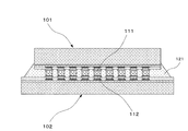
特に、図7に示すように、上側チップ101と下側チップ102同士を接続させるCoC(Chip on Chip)接続では、基板配線を介さずに上側チップ101と下側チップ102間を電気的に接続するため、配線長、容量の低減が可能である。
加えて、上側チップ101、下側チップ102のそれぞれに、数千個の径が数十μmのバンプ111、112を配置し、対向するバンプ111、112同士を接続している。このため、基板接続型のフリップチップ接続と比較して、バンド幅を飛躍的に増加させることが可能となる。この結果、CoC接続は伝送速度向上が可能となり、従来のSiPのデメリットを克服できる。
また、上側チップ101、下側チップ102間には封止樹脂121が充填されている。
このセミアディティブ法は、シード層を形成した後、このシード層上にレジスト膜を形成する。そして、バンプ形成位置のレジスト膜に開口部を形成するパターニングを行う。次いで、開口部内のシード層上に、電気めっき(電解めっき)法で金属層とはんだ層を形成した後、レジスト膜を除去する。さらに、余剰なシード層を除去するという工程を順に行い、金属層とはんだ層からなるバンプを形成する方法である(例えば、特許文献1、非特許文献1参照。)。
また、上記プロセスでは、余剰なシード層を除去した後、各金属層とはんだ層をフラックス層で被覆してはんだ層のリフロー処理を行い、はんだ層表面を曲面に形成している。このリフロー処理を行っても、初めに形成された金属層とはんだ層の高さが部分的に異なっているため、リフロー後の金属層とはんだ層を合わせたバンプの高さにばらつきを生じていた。
また、無電解めっきによって、各銅電極上に金属接続層を形成しているため、金属接続層は均一な厚さに形成される。通常、無電解めっきは、電解めっきのように電流密度の差が生じることがないので、めっき成長が、半導体チップの全域において均一になる。
たとえ金属接続層を形成した後に金属接続層をリフロー処理することがあっても、バリア層によって金属接続層の流れ出しが抑えられるので、金属接続層を含む各バンプの高さは、同等な高さが維持される。
よって、銅電極および金属接続層で形成される複数のバンプは、高さが同等なものに形成される。
よって、フリップチップ接続における歩留まりの向上、信頼性の向上が図れる。
よって、フリップチップ接続における歩留まりの向上、信頼性の向上が図れる半導体装置を製造できる。
この半導体チップ10の主面10Sには、上記集積回路素子(図示せず)、上記配線(図示せず)等に接続された、複数の電極パッド11が形成されている。
図面では、代表して一つの電極パッド11を示したが、本発明の半導体装置1では、半導体チップ10の主面10Sに例えば数千個の上記電極パッド11が形成されている。
上記電極パッド11は、例えばアルミニウム電極で形成されている。もちろん、アルミニウム以外の金属電極、例えば、銅電極、銅合金電極、アルミニウム合金電極等であってもよい。
上記各電極パッド11上の上記絶縁膜21には、開口部24が形成されている。
上記バンプ12は、上記開口部24を通じて上記電極パッド11に接続する銅電極13と、この銅電極13表面に形成された金属接続層14と、上記銅電極13および上記金属接続層14の側部および上記開口部24の内面に形成されたバリア層15を有する。
上記金属接続層14は、スズ、金、ニッケルのいずれかで形成されている。
上記バリア層15は、例えば、チタン膜、窒化チタン膜、タンタル膜、窒化タンタル膜の少なくとも1種で形成されている。例えば、絶縁膜21との密着性をよくするためのチタン膜と、このチタン膜表面に形成されたタンタル膜もしくは窒化タンタル膜との積層膜で形成することもできる。この場合、タンタル膜、窒化タンタル膜が主としてバリア層の機能を有する。このバリア層の機能としては、絶縁膜21中の酸素が銅電極13中に拡散して銅電極13が酸化されるのを防止するとともに、銅電極13の銅が絶縁膜21中に拡散するのを防止する。
そして、上記各銅電極13は同等の高さに形成されていて、上記各金属接続層14は同等の厚さに形成されている。
上記のように半導体装置1が構成されている。
図2に示すように、上記半導体装置1に形成されたバンプ12(12−1)と、本発明の構成を有する上記半導体装置1とは別の半導体装置2に形成されたバンプ12(12−2)とを対向させる。そして、一方の半導体装置、例えば半導体装置2を矢印方向にフェースダウンしてバンプ12−1、12−2同士を接続させる。なお、図面では、フェースダウンする状態を示した。
この場合、バンプ12(12−1)は全て高さが同等であり、バンプ12(12−2)も全て高さが同等であるから、全ての対向するバンプ12−1、12−2同士の接続が確実にできる。
したがって、接続不良が発生しなくなるという利点がある。
よって、フリップチップ接続における歩留まりの向上、信頼性の向上が図れる。
また図示はしていないが、半導体装置1、2間には封止樹脂が充填される。
また図示はしていないが、ウエハに形成された半導体チップは、通常の半導体チップであり、例えば、半導体基板に集積回路素子およびこの集積回路素子に接続する配線が形成され、保護膜により被覆されたものである。
図面では、代表して一つの電極パッド11を示したが、上記半導体チップ10の主面10Sに、例えば数百個ないし数千個の上記電極パッド11が形成されている。
上記電極パッド11は、例えばアルミニウム電極で形成されている。もちろん、アルミニウム以外の金属電極、例えば、銅電極、銅合金電極、アルミニウム合金電極等であってもよい。
上記エッチング後に上記レジストマスクを除去する。
この工程では、図4(2)に示すように、上記第1絶縁膜21上に、上記各第1開口部24が埋め込まれる第2絶縁膜25を形成する。
上記第2絶縁膜25は、その後に形成されるバンプの高さと同一の膜厚、もしくは、それより厚い膜厚とする。上記第2絶縁膜25は次工程以降のめっき、化学的機械研磨(CMP)後に除去できる材料で形成する。そのような材料は、例えば酸化シリコン膜がある。
この工程では、図4(3)に示すように、上記第2絶縁膜25上にレジスト塗布技術によりレジスト膜41を形成する。次いで、リソグラフィ技術(例えば露出、現像、ベーキング等)によって、上記第1開口部24上方に、例えば第1開口部24より大きい口径のレジスト開口部42を形成する。
この工程では、図5(4)に示すように、上記レジスト膜41をエッチングマスクに用いて、上記第2絶縁膜25に第2開口部26を形成する。このとき、第2絶縁膜25に埋め込まれた上記第1開口部24も再び開口される。したがって、上記第2開口部26の下部に連続して上記第1開口部24が形成される。
なお、図面は、第2開口部26を形成し、第1開口部24を再び開口している途中の状態を示している。
この工程では、図5(5)に示すように、上記第1、第2開口部24、26の内面および上記第2絶縁膜25の表面にバリア層15を形成する。
上記バリア層15は、例えば、チタン膜、窒化チタン膜、タンタル膜、窒化タンタル膜の少なくとも1種で形成される。例えば、絶縁膜21との密着性をよくするためのチタン膜と、このチタン膜表面に形成されたタンタル膜もしくは窒化タンタル膜との積層膜で形成することもできる。この場合、タンタル膜、窒化タンタル膜が主としてバリア層の機能を有する。このバリア層の機能としては、絶縁膜21中の酸素が後に形成される銅電極中に拡散して銅電極が酸化されるのを防止するとともに、後に形成される銅電極の銅が絶縁膜21、半導体チップ10等に拡散するのを防止する。
さらに、上記バリア層15の表面にめっきのシード層(図示せず)を形成する。このシード層には、例えば銅を用いる。
上記密着層、バリア層15、シード層等の成膜は、例えば化学気相成長(CVD)法、スパッタ法等のステップカバレッジに優れた成膜方法で行うことが好ましい。
この工程では、図5(6)に示すように、上記バリア層15を介して上記第1、第2開口部24、26の内部が埋め込まれる銅膜16を形成する。この銅膜16は、例えば上記銅のシード層をめっき種として電解めっきにより形成する。ここでは、電解めっきを用いることができる。それは、各第2開口部26において、めっき膜の膜厚にばらつきが生じてもかまわないからである。要するに、上記第1、第2開口部24、26の内部を完全に埋め込むことができればよい。もちろん、他の成膜方法によって、銅膜16を形成することも可能である。
この工程では、図6(7)に示すように、化学的機械研磨(CMP)によって上記第2絶縁膜25上の上記銅膜16(シード層も含む)および上記バリア層15を除去して、上記第1、第2開口部24、26内に上記バリア層15を介して上記銅膜16(上記銅のシード層も含む)からなる銅電極13を形成する。
なお、図面は、銅膜16を研磨していく途中の状態を示した。
この工程では、上記図6(8)に示すように、第2絶縁膜25を除去する。第2絶縁膜25が酸化シリコン膜の場合、フッ酸系薬液を使用し、ウエットエッチングにより除去する。その場合、第1絶縁膜21の窒化シリコン膜23がエッチングストッパ膜となる。
なお、図面は、第2絶縁膜25をエッチングする直前の状態を示した。
この工程では、図6(9)に示すように、上記銅電極13の銅を無電解めっき(例えば置換めっき、もしくは化学めっき)によって、上記銅電極13の上層部に金属接続層14を形成する。
上記金属接続層14は、スズ、金、ニッケルのいずれかで形成する。
なお、金(Au)、ニッケル(Ni)を形成する場合、さらに、上記銅電極13の表面の酸化防止のために、めっき液中に防食剤もしくは酸化防止剤を添加しても良い。
また、上記金属接続層14は、無電解めっきによって、スズ鉛合金、スズ銀合金等のはんだで形成することもできる。
以上のようにして、各電極パッド11上に接続するバンプ12が形成される。
また、無電解めっきによって、各銅電極13の上層部に金属接続層14を形成しているため、金属接続層は均一な厚さに形成される。通常、無電解めっきは、電解めっきのように電流密度の差が生じることがないので、めっき成長が、半導体チップ10の全域において均一になる。
したがって、銅電極13および金属接続層14で形成される複数のバンプ12は、高さが同等なものに形成される。
よって、フリップチップ接続における歩留まりの向上、信頼性の向上が図れる半導体装置を製造できる。
特に、上記従来技術のサイドエッチングの問題から、従来技術では数十μm以下の微細バンプの形成が困難であった。しかしながら、本発明では、現状技術の流用でサブミクロンオーダー、またはそれ以下の径のバンプ12の形成が可能となる。
Claims (6)
- 半導体チップと、
前記半導体チップの主面に形成された複数の電極パッドと、
前記半導体チップの主面に形成されていて前記各電極パッドを被覆する絶縁膜と、
前記各電極パッド上の前記絶縁膜に形成された開口部と、
前記絶縁膜上に前記各開口部を通じて前記各電極パッドに接続されたバンプを有し、
前記バンプは、
前記開口部を通じて前記電極パッドに接続する銅電極と、
前記銅電極上面に形成された金属接続層と、
前記銅電極および前記金属接続層の側部および前記開口部の内面に形成されたバリア層を有し、
前記各銅電極は同等の高さに形成され、
前記各金属接続層は同等の厚さに形成されている
半導体装置。 - 前記バリア層は、チタン膜、窒化チタン膜、タンタル膜、窒化タンタル膜の少なくとも1種で形成されている
請求項1記載の半導体装置。 - 前記金属接続層は、スズ、金、ニッケルのいずれかで形成されている
請求項1記載の半導体装置。 - 半導体チップの主面に複数の電極パッドを形成する工程と、
前記半導体チップの主面に前記各電極パッドを被覆する第1絶縁膜を形成する工程と、
前記電極パッド上の前記第1絶縁膜に第1開口部を形成する工程と、
前記第1絶縁膜の表面に前記各第1開口部が埋め込まれる第2絶縁膜を形成する工程と、
前記電極パッド上の前記第2絶縁膜に第2開口部を形成し、該第2開口部の下部に連続する前記第1開口部を再び開口する工程と、
前記第1、第2開口部の内面および前記第2絶縁膜の表面にバリア層を形成する工程と、
前記バリア層を介して前記第1、第2開口部の内部が埋め込まれる銅膜を形成する工程と、
化学的機械研磨によって前記第2絶縁膜上の前記銅膜および前記バリア層を除去して、前記第1、第2開口部内に前記バリア層を介して前記銅膜からなる銅電極を形成する工程と、
前記第2絶縁膜を除去する工程と、
無電解めっきによって前記銅電極上に金属接続層を形成する工程を有する
半導体装置の製造方法。 - 前記バリア層は、チタン膜、窒化チタン膜、タンタル膜、窒化タンタル膜の少なくとも1種で形成する
請求項4記載の半導体装置の製造方法。 - 前記金属接続層は、スズ、金、ニッケルのいずれかで形成する
請求項4記載の半導体装置の製造方法。
Priority Applications (1)
| Application Number | Priority Date | Filing Date | Title |
|---|---|---|---|
| JP2008208825A JP5277788B2 (ja) | 2008-08-14 | 2008-08-14 | 半導体装置およびその製造方法 |
Applications Claiming Priority (1)
| Application Number | Priority Date | Filing Date | Title |
|---|---|---|---|
| JP2008208825A JP5277788B2 (ja) | 2008-08-14 | 2008-08-14 | 半導体装置およびその製造方法 |
Publications (2)
| Publication Number | Publication Date |
|---|---|
| JP2010045234A true JP2010045234A (ja) | 2010-02-25 |
| JP5277788B2 JP5277788B2 (ja) | 2013-08-28 |
Family
ID=42016373
Family Applications (1)
| Application Number | Title | Priority Date | Filing Date |
|---|---|---|---|
| JP2008208825A Expired - Fee Related JP5277788B2 (ja) | 2008-08-14 | 2008-08-14 | 半導体装置およびその製造方法 |
Country Status (1)
| Country | Link |
|---|---|
| JP (1) | JP5277788B2 (ja) |
Cited By (4)
| Publication number | Priority date | Publication date | Assignee | Title |
|---|---|---|---|---|
| JP2012116880A (ja) * | 2010-11-29 | 2012-06-21 | Henkel Japan Ltd | 屋外用ウレタン接着剤 |
| JP2012231130A (ja) * | 2011-04-25 | 2012-11-22 | Samsung Electro-Mechanics Co Ltd | パッケージ基板及びその製造方法 |
| JP5636122B1 (ja) * | 2013-11-06 | 2014-12-03 | チップモス テクノロジーズ インコーポレイテッドChipmos Technologies Inc. | 半導体構造およびその製造方法 |
| JP2018046148A (ja) * | 2016-09-14 | 2018-03-22 | 富士通株式会社 | 端子構造、半導体装置、電子装置及び端子の形成方法 |
Citations (7)
| Publication number | Priority date | Publication date | Assignee | Title |
|---|---|---|---|---|
| JP2000294585A (ja) * | 1999-04-01 | 2000-10-20 | Nec Corp | バンプ構造及びその形成方法 |
| JP2003273158A (ja) * | 2002-01-18 | 2003-09-26 | Internatl Business Mach Corp <Ibm> | 高密度微小接続システム |
| JP2004193517A (ja) * | 2002-12-13 | 2004-07-08 | Seiko Epson Corp | 半導体チップ、半導体チップの製造方法、半導体実装基板、電子デバイスおよび電子機器 |
| JP2006245289A (ja) * | 2005-03-03 | 2006-09-14 | Casio Micronics Co Ltd | 半導体装置及び実装構造体 |
| JP2006279062A (ja) * | 2006-05-25 | 2006-10-12 | Nec Corp | 半導体素子および半導体装置 |
| JP2008004967A (ja) * | 2007-09-25 | 2008-01-10 | Seiko Epson Corp | 端子電極、半導体装置およびモジュール |
| JP2008182059A (ja) * | 2007-01-25 | 2008-08-07 | Casio Comput Co Ltd | 半導体装置およびその製造方法 |
-
2008
- 2008-08-14 JP JP2008208825A patent/JP5277788B2/ja not_active Expired - Fee Related
Patent Citations (7)
| Publication number | Priority date | Publication date | Assignee | Title |
|---|---|---|---|---|
| JP2000294585A (ja) * | 1999-04-01 | 2000-10-20 | Nec Corp | バンプ構造及びその形成方法 |
| JP2003273158A (ja) * | 2002-01-18 | 2003-09-26 | Internatl Business Mach Corp <Ibm> | 高密度微小接続システム |
| JP2004193517A (ja) * | 2002-12-13 | 2004-07-08 | Seiko Epson Corp | 半導体チップ、半導体チップの製造方法、半導体実装基板、電子デバイスおよび電子機器 |
| JP2006245289A (ja) * | 2005-03-03 | 2006-09-14 | Casio Micronics Co Ltd | 半導体装置及び実装構造体 |
| JP2006279062A (ja) * | 2006-05-25 | 2006-10-12 | Nec Corp | 半導体素子および半導体装置 |
| JP2008182059A (ja) * | 2007-01-25 | 2008-08-07 | Casio Comput Co Ltd | 半導体装置およびその製造方法 |
| JP2008004967A (ja) * | 2007-09-25 | 2008-01-10 | Seiko Epson Corp | 端子電極、半導体装置およびモジュール |
Cited By (4)
| Publication number | Priority date | Publication date | Assignee | Title |
|---|---|---|---|---|
| JP2012116880A (ja) * | 2010-11-29 | 2012-06-21 | Henkel Japan Ltd | 屋外用ウレタン接着剤 |
| JP2012231130A (ja) * | 2011-04-25 | 2012-11-22 | Samsung Electro-Mechanics Co Ltd | パッケージ基板及びその製造方法 |
| JP5636122B1 (ja) * | 2013-11-06 | 2014-12-03 | チップモス テクノロジーズ インコーポレイテッドChipmos Technologies Inc. | 半導体構造およびその製造方法 |
| JP2018046148A (ja) * | 2016-09-14 | 2018-03-22 | 富士通株式会社 | 端子構造、半導体装置、電子装置及び端子の形成方法 |
Also Published As
| Publication number | Publication date |
|---|---|
| JP5277788B2 (ja) | 2013-08-28 |
Similar Documents
| Publication | Publication Date | Title |
|---|---|---|
| US11515288B2 (en) | Protective layer for contact pads in fan-out interconnect structure and method of forming same | |
| US7323406B2 (en) | Elevated bond-pad structure for high-density flip-clip packaging and a method of fabricating the structures | |
| US6727590B2 (en) | Semiconductor device with internal bonding pad | |
| TWI582937B (zh) | 封裝結構 | |
| US9318455B2 (en) | Method of forming a plurality of bumps on a substrate and method of forming a chip package | |
| US9048225B2 (en) | Semiconductor device and method for manufacturing semiconductor device | |
| US7282433B2 (en) | Interconnect structures with bond-pads and methods of forming bump sites on bond-pads | |
| TWI442524B (zh) | 覆晶封裝以及半導體晶片 | |
| KR100714818B1 (ko) | 반도체 장치 및 그 제조 방법 | |
| CN102222647B (zh) | 半导体裸片及形成导电元件的方法 | |
| US10163862B2 (en) | Package structure and method for forming same | |
| TWI607495B (zh) | 半導體元件結構及其形成方法 | |
| US20070087544A1 (en) | Method for forming improved bump structure | |
| TW201203483A (en) | Recessed pillar structure and manufacturing method thereof | |
| US20060160346A1 (en) | Substrate bump formation | |
| TW201041057A (en) | Semiconductor device and method of forming enhanced UBM structure for improving solder joint reliability | |
| JP6547745B2 (ja) | 半導体装置およびその製造方法 | |
| TW201820464A (zh) | 半導體裝置的製造方法 | |
| JP5277788B2 (ja) | 半導体装置およびその製造方法 | |
| JP3735547B2 (ja) | 半導体装置及びその製造方法 | |
| JP4342892B2 (ja) | 半導体装置およびその製造方法 | |
| TWI419285B (zh) | 基板上的凸塊結構與其形成方法 | |
| JP6544354B2 (ja) | 半導体装置の製造方法 | |
| JP4393343B2 (ja) | 半導体装置の製造方法 | |
| WO2021103489A1 (zh) | 半导体结构及其制造方法 |
Legal Events
| Date | Code | Title | Description |
|---|---|---|---|
| RD02 | Notification of acceptance of power of attorney |
Free format text: JAPANESE INTERMEDIATE CODE: A7422 Effective date: 20100908 |
|
| A621 | Written request for application examination |
Free format text: JAPANESE INTERMEDIATE CODE: A621 Effective date: 20110803 |
|
| A977 | Report on retrieval |
Free format text: JAPANESE INTERMEDIATE CODE: A971007 Effective date: 20120727 |
|
| A131 | Notification of reasons for refusal |
Free format text: JAPANESE INTERMEDIATE CODE: A131 Effective date: 20120731 |
|
| A521 | Written amendment |
Free format text: JAPANESE INTERMEDIATE CODE: A523 Effective date: 20120921 |
|
| A131 | Notification of reasons for refusal |
Free format text: JAPANESE INTERMEDIATE CODE: A131 Effective date: 20130115 |
|
| A521 | Written amendment |
Free format text: JAPANESE INTERMEDIATE CODE: A523 Effective date: 20130305 |
|
| TRDD | Decision of grant or rejection written | ||
| A01 | Written decision to grant a patent or to grant a registration (utility model) |
Free format text: JAPANESE INTERMEDIATE CODE: A01 Effective date: 20130423 |
|
| A61 | First payment of annual fees (during grant procedure) |
Free format text: JAPANESE INTERMEDIATE CODE: A61 Effective date: 20130506 |
|
| LAPS | Cancellation because of no payment of annual fees |