JP2010040968A - 露光方法、半導体装置の製造方法、及びマスクデータの作成方法 - Google Patents
露光方法、半導体装置の製造方法、及びマスクデータの作成方法 Download PDFInfo
- Publication number
- JP2010040968A JP2010040968A JP2008205279A JP2008205279A JP2010040968A JP 2010040968 A JP2010040968 A JP 2010040968A JP 2008205279 A JP2008205279 A JP 2008205279A JP 2008205279 A JP2008205279 A JP 2008205279A JP 2010040968 A JP2010040968 A JP 2010040968A
- Authority
- JP
- Japan
- Prior art keywords
- mask pattern
- exposure
- best focus
- wafer
- photoresist
- Prior art date
- Legal status (The legal status is an assumption and is not a legal conclusion. Google has not performed a legal analysis and makes no representation as to the accuracy of the status listed.)
- Granted
Links
Images


Classifications
-
- G—PHYSICS
- G03—PHOTOGRAPHY; CINEMATOGRAPHY; ANALOGOUS TECHNIQUES USING WAVES OTHER THAN OPTICAL WAVES; ELECTROGRAPHY; HOLOGRAPHY
- G03F—PHOTOMECHANICAL PRODUCTION OF TEXTURED OR PATTERNED SURFACES, e.g. FOR PRINTING, FOR PROCESSING OF SEMICONDUCTOR DEVICES; MATERIALS THEREFOR; ORIGINALS THEREFOR; APPARATUS SPECIALLY ADAPTED THEREFOR
- G03F7/00—Photomechanical, e.g. photolithographic, production of textured or patterned surfaces, e.g. printing surfaces; Materials therefor, e.g. comprising photoresists; Apparatus specially adapted therefor
- G03F7/70—Microphotolithographic exposure; Apparatus therefor
- G03F7/70425—Imaging strategies, e.g. for increasing throughput or resolution, printing product fields larger than the image field or compensating lithography- or non-lithography errors, e.g. proximity correction, mix-and-match, stitching or double patterning
- G03F7/70433—Layout for increasing efficiency or for compensating imaging errors, e.g. layout of exposure fields for reducing focus errors; Use of mask features for increasing efficiency or for compensating imaging errors
Landscapes
- Physics & Mathematics (AREA)
- General Physics & Mathematics (AREA)
- Exposure And Positioning Against Photoresist Photosensitive Materials (AREA)
- Exposure Of Semiconductors, Excluding Electron Or Ion Beam Exposure (AREA)
Abstract
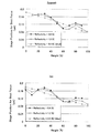
【解決手段】露光実行条件に基づいて、第1のマスクパターン及び第2のマスクパターンが形成されたマスクに光を照射し、投影レンズを介して前記第1のマスクパターン及び第2のマスクパターンの像を下層膜材料及びフォトレジストが順に積層されたウェーハに投影する露光方法であって、前記露光実行条件は、所定の露光条件で露光を行う場合に、前記フォトレジスト及び前記下層膜材料の膜厚及び光学特性を用いて予測された、前記第1のマスクパターンの像についてベストフォーカスとなる前記ウェーハの位置と、前記第2のマスクパターンの像についてベストフォーカスとなる前記ウェーハの位置との差が、所定の範囲内の値となるように前記所定の露光条件が変更された条件である。
【選択図】図2
Description
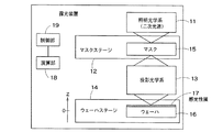
12 マスクステージ
13 投影光学系(レンズ)
14 ウェーハステージ
15 マスク
16 ウェーハ
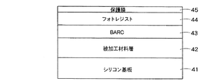
17 感光性膜
18 演算部
19 制御部
Claims (5)
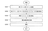
- 露光装置を用いて第1及び第2のマスクパターンを含むマスクパターンの像をウェーハ上に形成する半導体装置の製造方法であって、
前記第1のマスクパターンの像についてベストフォーカスとなる前記ウェーハの位置と、前記第2のマスクパターンの像についてベストフォーカスとなる前記ウェーハの位置との差が所定の範囲内の値となるように投影レンズの収差値を調整した前記露光装置を用いて、前記マスクパターンの像を前記ウェーハに形成する工程を備えることを特徴とする半導体装置の製造方法。 - 露光実行条件に基づいて、第1のマスクパターン及び第2のマスクパターンが形成されたマスクに光を照射し、投影レンズを介して前記第1のマスクパターン及び第2のマスクパターンの像を下層膜材料及びフォトレジストが順に積層されたウェーハに投影する露光方法であって、
前記露光実行条件は、
所定の露光条件で露光を行う場合に、前記フォトレジスト及び前記下層膜材料の膜厚及び光学特性を用いて予測された、前記第1のマスクパターンの像についてベストフォーカスとなる前記ウェーハの位置と、前記第2のマスクパターンの像についてベストフォーカスとなる前記ウェーハの位置との差が、所定の範囲内の値となるように前記所定の露光条件が変更された条件であることを特徴とする露光方法。 - 前記光学特性は、前記光の波長に対する屈折率及び消衰係数であることを特徴とする請求項2に記載の露光方法。
- 前記所定の露光条件の変更では、前記投影レンズの収差の値が調整されることを特徴とする請求項2又は3に記載の露光方法。
- 露光処理時に二次光源から発した光が照射され、形成された第1のマスクパターン及び第2のマスクパターンの像が投影レンズを介して、ウェーハ上に順に積層された下層膜材料及びフォトレジストの前記フォトレジストに投影されるマスクの製造に用いられるマスクデータの作成方法であって、
前記フォトレジスト及び前記下層膜材料の膜厚及び光学特性、前記二次光源の形状、及び所定の前記投影レンズの収差を用いて、前記第1のマスクパターンの像についてベストフォーカスとなる前記ウェーハの第1の位置と、前記第2のマスクパターンの像についてベストフォーカスとなる前記ウェーハの第2の位置とを予測し、
前記第1の位置と前記第2の位置との差が所定の範囲内の値となるように前記収差を調整し、
前記調整後の収差を用いてOPC処理を実行することを特徴とするマスクデータの作成方法。
Priority Applications (2)
| Application Number | Priority Date | Filing Date | Title |
|---|---|---|---|
| JP2008205279A JP4703693B2 (ja) | 2008-08-08 | 2008-08-08 | 露光方法、半導体装置の製造方法、及びマスクデータの作成方法 |
| US12/536,758 US8142960B2 (en) | 2008-08-08 | 2009-08-06 | Exposure method, mask data producing method, and semiconductor device manufacturing method |
Applications Claiming Priority (1)
| Application Number | Priority Date | Filing Date | Title |
|---|---|---|---|
| JP2008205279A JP4703693B2 (ja) | 2008-08-08 | 2008-08-08 | 露光方法、半導体装置の製造方法、及びマスクデータの作成方法 |
Publications (2)
| Publication Number | Publication Date |
|---|---|
| JP2010040968A true JP2010040968A (ja) | 2010-02-18 |
| JP4703693B2 JP4703693B2 (ja) | 2011-06-15 |
Family
ID=41653242
Family Applications (1)
| Application Number | Title | Priority Date | Filing Date |
|---|---|---|---|
| JP2008205279A Active JP4703693B2 (ja) | 2008-08-08 | 2008-08-08 | 露光方法、半導体装置の製造方法、及びマスクデータの作成方法 |
Country Status (2)
| Country | Link |
|---|---|
| US (1) | US8142960B2 (ja) |
| JP (1) | JP4703693B2 (ja) |
Cited By (2)
| Publication number | Priority date | Publication date | Assignee | Title |
|---|---|---|---|---|
| JP2014165398A (ja) * | 2013-02-26 | 2014-09-08 | Toshiba Corp | フォーカス位置調整装置、レチクル、フォーカス位置調整プログラムおよび半導体装置の製造方法 |
| JP2019508734A (ja) * | 2016-02-22 | 2019-03-28 | エーエスエムエル ネザーランズ ビー.ブイ. | メトロロジデータへの寄与の分離 |
Families Citing this family (5)
| Publication number | Priority date | Publication date | Assignee | Title |
|---|---|---|---|---|
| WO2007086511A1 (ja) * | 2006-01-30 | 2007-08-02 | Nikon Corporation | 処理条件決定方法及び装置、表示方法及び装置、処理装置、測定装置及び露光装置、基板処理システム、並びにプログラム及び情報記録媒体 |
| JP6537992B2 (ja) * | 2016-03-30 | 2019-07-03 | 東京エレクトロン株式会社 | 基板処理装置、基板処理装置の制御方法、及び基板処理システム |
| DE102017115365B4 (de) | 2017-07-10 | 2020-10-15 | Carl Zeiss Smt Gmbh | Inspektionsvorrichtung für Masken für die Halbleiterlithographie und Verfahren |
| CN113917799B (zh) * | 2021-09-28 | 2023-11-10 | 上海华力集成电路制造有限公司 | 一种改善曝光焦距均匀性的方法 |
| CN120949503B (zh) * | 2025-10-16 | 2025-12-30 | 合肥晶合集成电路股份有限公司 | 掩膜版组及其制造方法、掩膜版成像偏差校正方法及系统 |
Citations (6)
| Publication number | Priority date | Publication date | Assignee | Title |
|---|---|---|---|---|
| JPH11307431A (ja) * | 1998-04-23 | 1999-11-05 | Sony Corp | 半導体装置の製造方法 |
| JP2004047755A (ja) * | 2002-07-12 | 2004-02-12 | Renesas Technology Corp | 露光条件決定システム |
| JP2004103674A (ja) * | 2002-09-06 | 2004-04-02 | Renesas Technology Corp | 半導体集積回路装置の製造方法 |
| JP2005158819A (ja) * | 2003-11-20 | 2005-06-16 | Elpida Memory Inc | 露光方法 |
| JP2006073709A (ja) * | 2004-09-01 | 2006-03-16 | Sony Corp | 多層反射防止膜 |
| JP2006344648A (ja) * | 2005-06-07 | 2006-12-21 | Matsushita Electric Ind Co Ltd | 露光方法 |
Family Cites Families (4)
| Publication number | Priority date | Publication date | Assignee | Title |
|---|---|---|---|---|
| US6208748B1 (en) * | 2000-01-05 | 2001-03-27 | Intel Corporation | Monitoring focus of a lens imaging system based on astigmatism |
| JP2002184675A (ja) | 2000-12-18 | 2002-06-28 | Nec Corp | 露光装置の投影レンズの球面収差の修正方法 |
| US6880135B2 (en) * | 2001-11-07 | 2005-04-12 | Synopsys, Inc. | Method of incorporating lens aberration information into various process flows |
| JP4068531B2 (ja) * | 2003-08-20 | 2008-03-26 | 株式会社東芝 | Opcを用いたパターン寸法の補正方法及び検証方法、マスクの作成方法及び半導体装置の製造方法、並びに該補正方法を実行するシステム及びプログラム |
-
2008
- 2008-08-08 JP JP2008205279A patent/JP4703693B2/ja active Active
-
2009
- 2009-08-06 US US12/536,758 patent/US8142960B2/en active Active
Patent Citations (6)
| Publication number | Priority date | Publication date | Assignee | Title |
|---|---|---|---|---|
| JPH11307431A (ja) * | 1998-04-23 | 1999-11-05 | Sony Corp | 半導体装置の製造方法 |
| JP2004047755A (ja) * | 2002-07-12 | 2004-02-12 | Renesas Technology Corp | 露光条件決定システム |
| JP2004103674A (ja) * | 2002-09-06 | 2004-04-02 | Renesas Technology Corp | 半導体集積回路装置の製造方法 |
| JP2005158819A (ja) * | 2003-11-20 | 2005-06-16 | Elpida Memory Inc | 露光方法 |
| JP2006073709A (ja) * | 2004-09-01 | 2006-03-16 | Sony Corp | 多層反射防止膜 |
| JP2006344648A (ja) * | 2005-06-07 | 2006-12-21 | Matsushita Electric Ind Co Ltd | 露光方法 |
Cited By (3)
| Publication number | Priority date | Publication date | Assignee | Title |
|---|---|---|---|---|
| JP2014165398A (ja) * | 2013-02-26 | 2014-09-08 | Toshiba Corp | フォーカス位置調整装置、レチクル、フォーカス位置調整プログラムおよび半導体装置の製造方法 |
| US8910096B2 (en) | 2013-02-26 | 2014-12-09 | Kabushiki Kaisha Toshiba | Focus position adjusting apparatus, reticle, focus position adjusting program, and method of manufacturing semiconductor device |
| JP2019508734A (ja) * | 2016-02-22 | 2019-03-28 | エーエスエムエル ネザーランズ ビー.ブイ. | メトロロジデータへの寄与の分離 |
Also Published As
| Publication number | Publication date |
|---|---|
| US8142960B2 (en) | 2012-03-27 |
| US20100035167A1 (en) | 2010-02-11 |
| JP4703693B2 (ja) | 2011-06-15 |
Similar Documents
| Publication | Publication Date | Title |
|---|---|---|
| JP4703693B2 (ja) | 露光方法、半導体装置の製造方法、及びマスクデータの作成方法 | |
| US7094507B2 (en) | Method for determining an optimal absorber stack geometry of a lithographic reflection mask | |
| KR102101837B1 (ko) | 포토마스크, 포토마스크의 레지스트레이션 에러 보정 방법, 포토마스크를 이용하여 제조된 집적 회로 및 그 제조 방법 | |
| US8029954B2 (en) | Exposure method and memory medium storing computer program | |
| KR101618405B1 (ko) | 마스크 패턴 생성 방법 | |
| JP2007305972A (ja) | 露光条件設定方法及び半導体デバイスの製造方法 | |
| US20080304029A1 (en) | Method and System for Adjusting an Optical Model | |
| JP2010128279A (ja) | パターン作成方法及びパターン検証プログラム | |
| US9223911B2 (en) | Optical model employing phase transmission values for sub-resolution assist features | |
| US20080153009A1 (en) | Exposure mask, optical proximity correction device, optical proximity correction method, manufacturing method of semiconductor device, and optical proximity correction program | |
| JP2005236074A (ja) | マスクパターン補正方法、露光用マスクおよびマスク製造方法 | |
| JP6614614B2 (ja) | 反射マスクおよびパターン形成方法 | |
| US7807323B2 (en) | Exposure condition setting method, semiconductor device manufacturing method, and exposure condition setting program | |
| US20210048758A1 (en) | Alignment mark positioning in a lithographic process | |
| JP2010251500A (ja) | 半導体デバイスの製造方法及び露光条件決定プログラム | |
| US7611806B2 (en) | Sub-wavelength diffractive elements to reduce corner rounding | |
| JP2009259976A (ja) | 露光方法およびそれを用いた半導体デバイスの製造方法 | |
| JP4790350B2 (ja) | 露光用マスク及び露光用マスクの製造方法 | |
| CN100529969C (zh) | 光掩模的判定方法以及半导体器件的制造方法 | |
| JP2010258145A (ja) | 半導体デバイスの製造方法 | |
| JP2005340493A (ja) | マスクパターン補正方法、露光用マスクおよびマスク製造方法 | |
| Arisawa et al. | EUV flare correction for the half-pitch 22nm node | |
| US11415876B2 (en) | Method of fabricating a photomask | |
| JPH1172924A (ja) | パターン形成方法 | |
| JP2005072309A (ja) | マスクパターン補正方法、露光用マスクおよびマスク製造方法 |
Legal Events
| Date | Code | Title | Description |
|---|---|---|---|
| A621 | Written request for application examination |
Free format text: JAPANESE INTERMEDIATE CODE: A621 Effective date: 20100802 |
|
| A977 | Report on retrieval |
Free format text: JAPANESE INTERMEDIATE CODE: A971007 Effective date: 20101029 |
|
| A131 | Notification of reasons for refusal |
Free format text: JAPANESE INTERMEDIATE CODE: A131 Effective date: 20101102 |
|
| A521 | Request for written amendment filed |
Free format text: JAPANESE INTERMEDIATE CODE: A523 Effective date: 20101221 |
|
| TRDD | Decision of grant or rejection written | ||
| A01 | Written decision to grant a patent or to grant a registration (utility model) |
Free format text: JAPANESE INTERMEDIATE CODE: A01 Effective date: 20110208 |
|
| A61 | First payment of annual fees (during grant procedure) |
Free format text: JAPANESE INTERMEDIATE CODE: A61 Effective date: 20110308 |
|
| R151 | Written notification of patent or utility model registration |
Ref document number: 4703693 Country of ref document: JP Free format text: JAPANESE INTERMEDIATE CODE: R151 |
|
| S111 | Request for change of ownership or part of ownership |
Free format text: JAPANESE INTERMEDIATE CODE: R313111 |
|
| R350 | Written notification of registration of transfer |
Free format text: JAPANESE INTERMEDIATE CODE: R350 |
|
| S111 | Request for change of ownership or part of ownership |
Free format text: JAPANESE INTERMEDIATE CODE: R313111 |
|
| R350 | Written notification of registration of transfer |
Free format text: JAPANESE INTERMEDIATE CODE: R350 |