JP2010034249A - Processing apparatus for semiconductor wafer - Google Patents
Processing apparatus for semiconductor wafer Download PDFInfo
- Publication number
- JP2010034249A JP2010034249A JP2008194336A JP2008194336A JP2010034249A JP 2010034249 A JP2010034249 A JP 2010034249A JP 2008194336 A JP2008194336 A JP 2008194336A JP 2008194336 A JP2008194336 A JP 2008194336A JP 2010034249 A JP2010034249 A JP 2010034249A
- Authority
- JP
- Japan
- Prior art keywords
- semiconductor wafer
- spinner
- cleaning
- wafer
- grinding
- Prior art date
- Legal status (The legal status is an assumption and is not a legal conclusion. Google has not performed a legal analysis and makes no representation as to the accuracy of the status listed.)
- Granted
Links
- 239000004065 semiconductor Substances 0.000 title claims abstract description 119
- 238000004140 cleaning Methods 0.000 claims abstract description 40
- 238000000034 method Methods 0.000 claims abstract description 24
- 238000001035 drying Methods 0.000 claims abstract description 16
- 239000013078 crystal Substances 0.000 claims abstract description 9
- 238000005498 polishing Methods 0.000 claims description 12
- 230000002093 peripheral effect Effects 0.000 claims description 5
- 235000012431 wafers Nutrition 0.000 description 126
- 230000007246 mechanism Effects 0.000 description 13
- 230000001681 protective effect Effects 0.000 description 4
- XUIMIQQOPSSXEZ-UHFFFAOYSA-N Silicon Chemical compound [Si] XUIMIQQOPSSXEZ-UHFFFAOYSA-N 0.000 description 3
- 229910052710 silicon Inorganic materials 0.000 description 3
- 239000010703 silicon Substances 0.000 description 3
- XLYOFNOQVPJJNP-UHFFFAOYSA-N water Substances O XLYOFNOQVPJJNP-UHFFFAOYSA-N 0.000 description 2
- 238000005452 bending Methods 0.000 description 1
- 229910010293 ceramic material Inorganic materials 0.000 description 1
- 238000005259 measurement Methods 0.000 description 1
- 239000013585 weight reducing agent Substances 0.000 description 1
Images


Abstract
Description
本発明は、外周に結晶方位を示すマークを備えた半導体ウエーハを研削又は研磨した後に次工程へ搬出する半導体ウエーハの加工装置に関する。 The present invention relates to a semiconductor wafer processing apparatus for grinding or polishing a semiconductor wafer having a crystal orientation mark on its outer periphery and then carrying it out to the next process.
IC、LSI等のデバイスが表面に形成され、個々のデバイスが分割予定ラインによって区画された半導体ウエーハは研削・研磨装置によって裏面が研削又は研磨されて所望の厚みへ加工された後、ダイシング装置等によって分割予定ラインが切削されて個々のデバイスに分割され、分割されたデバイスは携帯電話、パソコン等の電気機器に広く利用されている。 A semiconductor wafer in which devices such as IC and LSI are formed on the surface, and each device is defined by lines to be divided is ground or polished by a grinding / polishing device and processed to a desired thickness, and then a dicing device or the like The line to be divided is cut and divided into individual devices, and the divided devices are widely used in electric devices such as mobile phones and personal computers.
近年、電気機器の軽量化、小型化を達成するために、これら半導体ウエーハ等の被加工物を例えば、100μm以下更には50μm以下と非常に薄く研削することが要求されている。 In recent years, in order to achieve weight reduction and miniaturization of electrical equipment, it has been required to grind these workpieces such as semiconductor wafers to a very thin thickness of, for example, 100 μm or less and further 50 μm or less.
しかし、例えば50μm以下と非常に薄く研削された半導体ウエーハは破損し易く、ハンドリングが困難になるという問題がある。通常、裏面が研削又は研磨された半導体ウエーハは研削・研磨装置から搬出された後、ダイシング後のチップピックアップを容易にするために、ダイシングの前に環状フレームに装着されたダイシングテープに貼着される。 However, there is a problem that a semiconductor wafer ground to be very thin, for example, 50 μm or less, is easily damaged and is difficult to handle. Usually, a semiconductor wafer whose back surface is ground or polished is taken out from a grinding / polishing apparatus and then attached to a dicing tape mounted on an annular frame before dicing to facilitate chip pick-up after dicing. The
一方、ダイシング装置で半導体ウエーハを切削する際に、装置が自動で切削位置を検出できるようにダイシングテープへの貼着時にウエーハの向きを揃える必要がある。 On the other hand, when cutting a semiconductor wafer with a dicing machine, it is necessary to align the direction of the wafer when sticking to a dicing tape so that the machine can automatically detect the cutting position.
そこで一般に、研削又は研磨されたウエーハはテープ貼着装置へと搬送された後、テープ貼着装置の位置合わせテーブル上に載置されて所定の向きへ位置合わせされてから、テープマウント用テーブルへと搬送されてダイシングテープが貼着される。
ところが、薄い半導体ウエーハでは抗折強度が十分でないため、テーブルへ載置する際に破損してしまうことが多く、テーブルへの載置回数が多ければそれだけ破損の可能性は高くなる。 However, since the bending strength of a thin semiconductor wafer is not sufficient, it is often damaged when it is placed on a table, and the possibility of breakage increases as the number of times of placement on the table increases.
本発明はこのような点に鑑みてなされたものであり、その目的とするところは、研削又は研磨された半導体ウエーハを所定の向きに位置合わせした後、次工程へ搬出可能な半導体ウエーハの加工装置を提供することである。 The present invention has been made in view of these points, and an object of the present invention is to process a semiconductor wafer that can be taken out to the next process after the ground or polished semiconductor wafer is aligned in a predetermined direction. Is to provide a device.
請求項1記載の発明によると、外周に結晶方位を示すマークを備えた半導体ウエーハの裏面を研削又は研磨する半導体ウエーハの加工装置であって、回転可能な保持テーブルを有し、半導体ウエーハの該マークを検出して半導体ウエーハを所定の向きに位置付ける位置合わせ手段と、該位置合わせ手段で所定方向へ位置付けられた半導体ウエーハを回転可能に保持するチャックテーブルと、該位置合わせ手段から該チャックテーブルへ半導体ウエーハを搬入すると共に加工済のウエーハを該チャックテーブルから搬出する旋回可能な搬入・搬出手段と、該チャックテーブルに保持された半導体ウエーハの裏面を所望の厚みに研削又は研磨する加工手段と、研削又は研磨された半導体ウエーハを洗浄及びスピン乾燥するスピンナテーブルを有するスピンナ洗浄手段と、該スピンナ洗浄手段により洗浄及びスピン乾燥された半導体ウエーハを該スピンナテーブル上から次工程へ搬出する旋回可能な搬出手段とを備え、前記チャックテーブルは研削又は研磨終了時に一定位置で回転を停止させる第1定点停止手段を有し、前記スピンナ洗浄手段は半導体ウエーハの洗浄及びスピン乾燥終了時に該スピンナテーブルの回転を一定位置で停止させる第2定点停止手段を有しており、前記洗浄手段は該第2定点停止手段により前記スピンナテーブルの回転位置を検出して、半導体ウエーハの洗浄及びスピン乾燥後に該スピンナテーブルへの搬入時と同一位置に該スピンナテーブルを停止させた後、前記搬出手段で半導体ウエーハを該スピンナテーブル上から次工程へ搬出することを特徴とする半導体ウエーハの加工装置が提供される。 According to the first aspect of the present invention, there is provided a semiconductor wafer processing apparatus for grinding or polishing the back surface of a semiconductor wafer having a crystal orientation mark on its outer periphery, the semiconductor wafer processing apparatus having a rotatable holding table, Positioning means for detecting the mark and positioning the semiconductor wafer in a predetermined direction, a chuck table for rotatably holding the semiconductor wafer positioned in a predetermined direction by the positioning means, and the positioning means to the chuck table A swivelable loading / unloading means for loading a semiconductor wafer and unloading the processed wafer from the chuck table; a processing means for grinding or polishing the back surface of the semiconductor wafer held by the chuck table to a desired thickness; Has a spinner table for cleaning and spin drying ground or polished semiconductor wafers A spinner cleaning means; and a swivelable unloading means for unloading the semiconductor wafer cleaned and spin-dried by the spinner cleaning means from the spinner table to the next process. First fixed point stopping means for stopping rotation, and the spinner cleaning means has second fixed point stopping means for stopping rotation of the spinner table at a fixed position at the end of cleaning and spin drying of the semiconductor wafer, The cleaning means detects the rotation position of the spinner table by the second fixed point stop means, stops the spinner table at the same position as when the semiconductor wafer is loaded into the spinner table after cleaning and spin drying, and The semiconductor wafer is unloaded from the spinner table to the next process by unloading means. Processing apparatus body wafer is provided.
請求項2記載の発明によると、位置合わせ手段では半導体ウエーハのマークは検出するが、半導体ウエーハの所定方向への位置付けは実施しない。半導体ウエーハの所定方向への位置付けは洗浄手段で実施する。即ち洗浄手段では、半導体ウエーハの洗浄及びスピン乾燥終了時にスピンナテーブル上への半導体ウエーハの搬入時と同一方向にマークを位置付けた後、位置合わせ手段で検出された半導体ウエーハのマークの位置に基づいて、スピンナテーブル上で保持された半導体ウエーハを所定の向きに位置付けて搬出手段で次工程へ搬出する。 According to the second aspect of the present invention, the alignment means detects the mark of the semiconductor wafer, but does not position the semiconductor wafer in a predetermined direction. The semiconductor wafer is positioned in a predetermined direction by a cleaning means. That is, the cleaning means positions the mark in the same direction as when the semiconductor wafer is loaded onto the spinner table at the end of cleaning and spin drying of the semiconductor wafer, and then based on the position of the mark on the semiconductor wafer detected by the alignment means. Then, the semiconductor wafer held on the spinner table is positioned in a predetermined direction and is carried out to the next process by the carrying-out means.
好ましくは、半導体ウエーハの結晶方位を示すマークは半導体ウエーハの外周に形成された切欠き又は平坦部から構成される。位置合わせ手段は、保持テーブルに保持された半導体ウエーハの外周部の上方と下方に対峙して配設された発光部と受光部とからなる光検知器を備えている。 Preferably, the mark indicating the crystal orientation of the semiconductor wafer is formed by a notch or a flat portion formed on the outer periphery of the semiconductor wafer. The alignment means includes a light detector that includes a light emitting portion and a light receiving portion that are disposed above and below the outer peripheral portion of the semiconductor wafer held by the holding table.
請求項1記載の発明によると、位置合わせ手段で半導体ウエーハを所定の向きに位置付けることが可能であるため、ダイシングテープを貼着するテープマウント工程等の次工程で、再度半導体ウエーハの向きを揃えるステップを省略でき、半導体ウエーハの破損を低減できる。 According to the first aspect of the present invention, since the semiconductor wafer can be positioned in a predetermined direction by the alignment means, the direction of the semiconductor wafer is aligned again in the next process such as a tape mounting process for adhering the dicing tape. Steps can be omitted and damage to the semiconductor wafer can be reduced.
請求項2記載の発明によると、位置合わせ手段で半導体ウエーハのマークを検出し、このマークの位置に基づいて、スピンナテーブル上で半導体ウエーハを所定の向きに位置付けることが可能であるため、ダイシングテープを貼着するテープマウント工程等の次工程で、再度半導体ウエーハの向きを揃えるステップを省略でき、半導体ウエーハの破損を低減できる。 According to the second aspect of the present invention, since the mark of the semiconductor wafer is detected by the alignment means, and the semiconductor wafer can be positioned on the spinner table in a predetermined direction based on the position of the mark, the dicing tape In the next process such as a tape mounting process for attaching the semiconductor wafer, the step of aligning the direction of the semiconductor wafer again can be omitted, and the damage of the semiconductor wafer can be reduced.
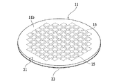
以下、本発明の実施形態を図面を参照して詳細に説明する。図1は所定の厚さに加工される前の第1実施形態の半導体ウエーハ11の斜視図である。図1に示す半導体ウエーハ11は、例えば厚さが700μmのシリコンウエーハから成っており、表面11aに複数のストリート13が格子状に形成されているとともに、該複数のストリート13によって区画された複数の領域にIC、LSI等のデバイス15が形成されている。
Hereinafter, embodiments of the present invention will be described in detail with reference to the drawings. FIG. 1 is a perspective view of the
このように構成された半導体ウエーハ11は、デバイス15が形成されているデバイス領域17と、デバイス領域17を囲繞する外周余剰領域19を備えている。また、半導体ウエーハ11の外周には、シリコンウエーハの結晶方位を示すマークとしてのノッチ(切欠き)21が形成されている。このノッチ21の方向は、一方の方向のストリート13に平行である。
The
半導体ウエーハ11の表面11aには、保護テープ貼着工程により保護テープ23が貼着される。従って、半導体ウエーハ11の研削時には、半導体ウエーハ11の表面11aは、保護テープ23によって保護され、図2に示すように裏面11bが露出する形態となる。
A
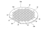
図3を参照すると、所定の厚さに加工される前の第2実施形態の半導体ウエーハ11Aの斜視図が示されている。半導体ウエーハ11Aは、第1実施形態の半導体ウエーハ11のノッチ21に代わり、オリエンテーションフラット部(平坦部)25を有している。この平坦部25もシリコンウエーハ11Aの結晶方位を示すマークとして機能する。平坦部25は一方の方向のストリート13と平行に形成されている。
Referring to FIG. 3, a perspective view of the
以下、このように形成された半導体ウエーハ11の裏面11bを所定厚さに研削する研削装置2を図4を参照して説明する。4は研削装置2のハウジングであり、ハウジング4の後方には二つのコラム6a6bが垂直に立設されている。
Hereinafter, a
コラム6aには、上下方向に伸びる一対のガイドレール(一本のみ図示)8が固定されている。この一対のガイドレール8に沿って粗研削ユニット10が上下方向に移動可能に装着されている。粗研削ユニット10は、そのハウジング20が一対のガイドレール8に沿って上下方向に移動する移動基台12に取り付けられている。
A pair of guide rails (only one is shown) 8 extending in the vertical direction is fixed to the
粗研削ユニット10は、ハウジング20と、ハウジング20中に回転可能に収容された図示しないスピンドルと、スピンドルを回転駆動するサーボモータ22と、スピンドルの先端に固定された複数の粗研削用の研削砥石26を有する研削ホイール24を含んでいる。
The
粗研削ユニット10は、粗研削ユニット10を一対の案内レール8に沿って上下方向に移動するボールねじ14とパルスモータ16とから構成される粗研削ユニット移動機構18を備えている。パルスモータ16をパルス駆動すると、ボールねじ14が回転し、移動基台12が上下方向に移動される。
The
他方のコラム6bにも、上下方向に伸びる一対のガイドレール(一本のみ図示)19が固定されている。この一対のガイドレール19に沿って仕上げ研削ユニット28が上下方向に移動可能に装着されている。
A pair of guide rails 19 (only one is shown) 19 extending in the vertical direction are also fixed to the
仕上げ研削ユニット28は、そのハウジング36が一対のガイドレール19に沿って上下方向に移動する図示しない移動基台に取り付けられている。仕上げ研削ユニット28は、ハウジング36と、ハウジング36中に回転可能に収容された図示しないスピンドルと、スピンドルを回転駆動するサーボモータ38と、スピンドルの先端に固定された仕上げ研削用の研削砥石42を有する研削ホイール40を含んでいる。
The
仕上げ研削ユニット28は、仕上げ研削ユニット28を一対の案内レール19に沿って上下方向に移動するボールねじ30とパルスモータ32とから構成される仕上げ研削ユニット移動機構34を備えている。パルスモータ32を駆動すると、ボールねじ30が回転し、仕上げ研削ユニット28が上下方向に移動される。
The
研削装置2は、コラム6a,6bの前側においてハウジング4の上面と略面一となるように配設されたターンテーブル44を具備している。ターンテーブル44は比較的大径の円盤状に形成されており、図示しない回転駆動機構によって矢印45で示す方向に回転される。
The
ターンテーブル44には、互いに円周方向に120°離間して3個のチャックテーブル46が水平面内で回転可能に配置されている。チャックテーブル46は、ポーラスセラミック材によって円盤状に形成された吸着チャックを有しており、吸着チャックの保持面上に載置されたウエーハを真空吸引手段を作動することにより吸引保持する。
On the
各チャックテーブル46は回転角度位置を検出する図示しないエンコーダを有している。各エンコーダは半導体ウエーハの研削又は研磨終了時にチャックテーブル46を一定位置で停止させる定点停止手段として機能する。 Each chuck table 46 has an encoder (not shown) that detects the rotational angle position. Each encoder functions as a fixed point stopping means for stopping the chuck table 46 at a fixed position at the end of grinding or polishing of the semiconductor wafer.
ターンテーブル44に配設された3個のチャックテーブル46は、ターンテーブル44が適宜回転することにより、ウエーハ搬入・搬出領域A、粗研削加工領域B、仕上げ研削加工領域C、及びウエーハ搬入・搬出領域Aに順次移動される。
The three chuck tables 46 arranged on the
ハウジング4の前側部分には、ウエーハカセット50と、リンク51及びハンド52を有するウエーハ搬送ロボット54と、ウエーハを位置合わせする位置合わせ手段56が配設されている。
A
位置合わせ手段56は、回転可能な保持テーブル(位置合わせテーブル)58と、保持テーブル58の回転角度位置を検出する図示しないエンコーダと、半径方向に移動可能な複数の位置決めピン59と、光検知器72とを含んでいる。
The positioning means 56 includes a rotatable holding table (positioning table) 58, an encoder (not shown) that detects the rotational angle position of the holding table 58, a plurality of
図5に示すように、光検知器72は支持部材74と、半導体ウエーハの外周部の上方と下方に対峙して配設されるように支持部材74に取り付けられた発光部76と受光部78を含んでいる。発光部76は例えばレーザダイオード(LD)等の発光素子から構成され、受光部78は例えばフォトダイオード(PD)等の受光素子から構成される。
As shown in FIG. 5, the
ハウジング4の前側部分には更に、ウエーハ搬入機構(ローディングアーム)60と、ウエーハ搬出機構(アンローディングアーム)62と、研削されたウエーハを洗浄及びスピン乾燥するスピンナ洗浄装置64と、スピンナ洗浄装置64で洗浄及びスピン乾燥された研削後のウエーハを次工程へ搬出する搬出手段66が配設されている。
The front portion of the housing 4 further includes a wafer loading mechanism (loading arm) 60, a wafer unloading mechanism (unloading arm) 62, a
スピンナ洗浄装置64は、研削された半導体ウエーハを吸引保持して回転するスピンナテーブル68と、スピンナテーブル68の回転角度位置を検出する図示しないエンコーダと、スピンナテーブル68に吸着保持された研削済みのウエーハに向けて洗浄水を供給する図示しない洗浄水供給ノズルと、カバー70とを有している。該エンコーダは、ウエーハの洗浄及びスピン乾燥終了時にスピンナテーブル68を一定位置で停止させる定点停止手段として機能する。
The
このように構成された研削装置2の研削作業について以下に説明する。ウエーハカセット50中に収容された半導体ウエーハは、ウエーハ搬送ロボット54の上下動作及び進退動作によって搬送され、位置合わせ手段56の保持テーブル58上に載置される。
The grinding operation of the grinding
位置合わせ手段56の保持テーブル58上に載置されたウエーハは、複数の位置決めピン59によって中心合わせが行われた後、保持テーブル58を回転して発光部76からの光をノッチ21を通して受光部78で受光することによりノッチ21の位置を検出する。
The wafer placed on the holding table 58 of the positioning means 56 is centered by a plurality of positioning pins 59, and then rotates the holding table 58 so that the light from the
このようにノッチ21の位置を検出した後、保持テーブル58を回転して半導体ウエーハ11を所定の向きに、即ち一連の研削工程を終えて搬出手段66でウエーハを次工程へ搬出する際、再度半導体ウエーハの向きを揃える必要のない向きに位置付ける。
After detecting the position of the
保持テーブル58上で所定の向きに位置付けられたウエーハは、ローディングアーム60の旋回動作によって、ウエーハ搬入・搬出領域Aに位置せしめられているチャックテーブル46に載置され、チャックテーブル46によって吸引保持される。
The wafer positioned in a predetermined direction on the holding table 58 is placed on the chuck table 46 positioned in the wafer loading / unloading area A by the swinging operation of the
次いで、ターンテーブル44が120度回転されて、ウエーハを保持したチャックテーブル46は粗研削加工領域Bに位置付けられる。このように位置付けられたウエーハに対して、チャックテーブル46を例えば300rpmで回転しつつ、研削ホイール24をチャックテーブル46と同一方向に例えば6000rpmで回転させるとともに粗研削ユニット移動機構18を作動して、粗研削用の研削砥石26をウエーハの裏面に接触させる。
Next, the
そして、研削ホイール24を所定の研削送り速度で下方に所定量研削送りして、ウエーハの粗研削を実施する。図示しない接触式の厚み測定ゲージによってウエーハの厚みを測定しながらウエーハを所望の厚みに仕上げる。
Then, the grinding
粗研削が終了したウエーハを保持したチャックテーブル46は、ターンテーブル44を120度回転することにより、仕上げ研削加工領域Cに位置付けられ、仕上げ研削用の研削砥石42を有する仕上げ研削ユニット28による仕上げ研削が実施される。
The chuck table 46 holding the wafer after the rough grinding is positioned in the finish grinding region C by rotating the
仕上げ研削を終了した半導体ウエーハを保持したチャックテーブル46は、ターンテーブル44を120度回転することにより、ウエーハ搬入・搬出領域Aに再び位置付けられる。
The chuck table 46 holding the semiconductor wafer after finish grinding is positioned again in the wafer loading / unloading area A by rotating the
チャックテーブル46に保持されているウエーハの吸引保持が解除されてから、ウエーハ搬出機構(アンローディングアーム)62の搬送パッド62bでウエーハが吸着されて、アンローディングアーム62が旋回することによりスピンナ洗浄装置64のスピンナテーブル68上にウエーハが搬送される。
After the suction and holding of the wafer held on the chuck table 46 is released, the wafer is adsorbed by the
本実施形態の研削装置2では、粗研削領域B及び仕上げ研削領域Cでの研削加工が終了すると、エンコーダによりチャックテーブル46の回転角度位置を検出して、チャックテーブル46は研削開始時と同一位置で停止される。
In the
ローディングアーム60の旋回角度及びアンローディングアーム62の旋回角度は予め決められているため、粗研削及び仕上げ研削を終了してアンローディングアーム62でスピンナテーブル68上に搬送されたウエーハは、所定の向きに位置付けられていることになる。ここで注意すべきは、スピンナテーブル68上の所定の向きは、位置合わせ手段56での所定の向きとは必ずしも一致する必要はない。
Since the turning angle of the
スピンナ洗浄装置64では、研削後の半導体ウエーハが洗浄されるとともにスピン乾燥される。本実施形態では、エンコーダによりスピンナテーブル68の回転角度位置を常に検出しているため、スピン乾燥終了後のウエーハの向きはアンローディングアーム62でスピンナテーブル68上に搬入されたウエーハの向きと一致するように制御される。
In the
ウエーハのスピン乾燥終了後、搬出手段66は所定の向きに位置付けられたウエーハを吸着して、例えばテープ貼着装置のテープマウント用テーブルへと搬送する。 After the spin drying of the wafer is completed, the carry-out means 66 sucks the wafer positioned in a predetermined direction and conveys it to, for example, a tape mount table of a tape sticking apparatus.
このテープ貼着装置では、図6に示すように、環状フレームFに外周部が貼着されたダイシングテープTに、ウエーハ11のノッチ21の向きが両側に切欠き88,90を有する環状フレームFの直線部分86に概略直交するように半導体ウエーハ11を貼着する。
In this tape applicator, as shown in FIG. 6, an annular frame
上述した実施形態では、位置合わせ手段56で半導体ウエーハ11のノッチ21を検出するとともに、このノッチ21の位置に基づいて半導体ウエーハ11を所定の向きに位置付けているが、位置合わせ手段56ではノッチ21の位置のみを検出するようにしても良い。
In the embodiment described above, the
この場合には、半導体ウエーハ11の洗浄及びスピン乾燥終了時に、スピンナテーブル68上への半導体ウエーハの搬入時と同一方向にノッチ21を位置付けた後、位置合わせ手段56で検出された半導体ウエーハのノッチ21の位置に基づいて、スピンナ洗浄装置64がスピンナテーブル68上で保持された半導体ウエーハ11を所定の向きに位置付ける。
In this case, at the end of cleaning and spin drying of the
上述した各実施形態では、位置合わせ手段56でノッチ21の位置を検出して半導体ウエーハ11を所定の向きに位置付けるか、或いは位置合わせ手段56ではノッチ21のみを検出して、スピンナ洗浄装置64で半導体ウエーハ11を所定の向きに位置付けることができるため、従来テープ貼着装置で必要であった位置合わせ用テーブルを省略することができる。よって、テープ貼着工程等の次工程で再度ウエーハの向きを揃えるステップを省略することができ、半導体ウエーハの破損を低減することができる。
In each of the embodiments described above, the position of the
尚、上述した実施形態の研削装置2は、粗研削ユニット10と仕上げ研削ユニット28を具備しているが、仕上げ研削ユニット28にかえて研磨バフが先端に装着された研磨ユニットを設けるようにすれば、研削されたウエーハの裏面を鏡面に研磨することもできる。
The grinding
また、上述した実施形態では、ウエーハ搬入機構(ローディングアーム)60及びウエーハ搬出機構(アンローディングアーム)62が設けられているが、ウエーハの搬入及び搬出を一つのウエーハ搬入・搬出機構で実施するようにしても良い。 In the above-described embodiment, the wafer carry-in mechanism (loading arm) 60 and the wafer carry-out mechanism (unloading arm) 62 are provided. However, the wafer carry-in and carry-out mechanisms are carried out by one wafer carry-in / out mechanism. Anyway.
2 研削装置
10 粗研削ユニット
11 半導体ウエーハ
13 ストリート
15 デバイス
21 ノッチ
28 仕上げ研削ユニット
44 ターンテーブル
46 チャックテーブル
56 位置合わせ手段
58 保持テーブル
60 ウエーハ搬入機構(ローディングアーム)
62 ウエーハ搬出機構(アンローディングアーム)
64 スピンナ洗浄装置
66 搬出手段
68 スピンナテーブル
2 Grinding
62 Wafer unloading mechanism (unloading arm)
64
Claims (5)
回転可能な保持テーブルを有し、半導体ウエーハの該マークを検出して半導体ウエーハを所定の向きに位置付ける位置合わせ手段と、
該位置合わせ手段で所定方向へ位置付けられた半導体ウエーハを回転可能に保持するチャックテーブルと、
該位置合わせ手段から該チャックテーブルへ半導体ウエーハを搬入すると共に加工済のウエーハを該チャックテーブルから搬出する旋回可能な搬入・搬出手段と、
該チャックテーブルに保持された半導体ウエーハの裏面を所望の厚みに研削又は研磨する加工手段と、
研削又は研磨された半導体ウエーハを洗浄及びスピン乾燥するスピンナテーブルを有するスピンナ洗浄手段と、
該スピンナ洗浄手段により洗浄及びスピン乾燥された半導体ウエーハを該スピンナテーブル上から次工程へ搬出する旋回可能な搬出手段とを備え、
前記チャックテーブルは研削又は研磨終了時に一定位置で回転を停止させる第1定点停止手段を有し、
前記スピンナ洗浄手段は半導体ウエーハの洗浄及びスピン乾燥終了時に該スピンナテーブルの回転を一定位置で停止させる第2定点停止手段を有しており、
前記洗浄手段は該第2定点停止手段により前記スピンナテーブルの回転位置を検出して、半導体ウエーハの洗浄及びスピン乾燥後に該スピンナテーブルへの搬入時と同一位置に該スピンナテーブルを停止させた後、前記搬出手段で半導体ウエーハを該スピンナテーブル上から次工程へ搬出することを特徴とする半導体ウエーハの加工装置。 A semiconductor wafer processing apparatus for grinding or polishing a back surface of a semiconductor wafer having a crystal orientation mark on its outer periphery,
A positioning means having a rotatable holding table, detecting the mark of the semiconductor wafer and positioning the semiconductor wafer in a predetermined direction;
A chuck table for rotatably holding the semiconductor wafer positioned in a predetermined direction by the alignment means;
Turnable loading / unloading means for loading the semiconductor wafer from the positioning means to the chuck table and unloading the processed wafer from the chuck table;
Processing means for grinding or polishing the back surface of the semiconductor wafer held on the chuck table to a desired thickness;
A spinner cleaning means having a spinner table for cleaning and spin drying a ground or polished semiconductor wafer;
A turnable unloading means for unloading the semiconductor wafer cleaned and spin-dried by the spinner cleaning means from the spinner table to the next process;
The chuck table has first fixed point stop means for stopping rotation at a fixed position at the end of grinding or polishing,
The spinner cleaning means has a second fixed point stop means for stopping the rotation of the spinner table at a fixed position when the semiconductor wafer cleaning and spin drying are completed.
The cleaning means detects the rotation position of the spinner table by the second fixed point stop means, and stops the spinner table at the same position as when the semiconductor wafer is loaded into the spinner table after cleaning and spin drying. An apparatus for processing a semiconductor wafer, wherein the semiconductor wafer is unloaded from the spinner table to the next process by the unloading means.
半導体ウエーハの該マークを検出し、該半導体ウエーハの中心を所定位置に位置付ける保持テーブルを有する位置合わせ手段と、
半導体ウエーハを回転可能に保持するチャックテーブルと、
該位置合わせ手段から半導体ウエーハを該チャックテーブルに搬入すると共に加工済のウエーハを該チャックテーブルから搬出する旋回可能な搬入・搬出手段と、
該チャックテーブルに保持された半導体ウエーハの裏面を所望の厚みに研削又は研磨する加工手段と、
研削又は研磨された半導体ウエーハを洗浄及びスピン乾燥するスピンナテーブルを有するスピンナ洗浄手段と、
該スピンナ洗浄手段により洗浄及びスピン乾燥された半導体ウエーハを該スピンナテーブル上から次工程へ搬出する旋回可能な搬出手段とを具備し、
前記チャックテーブルは研削又は研磨終了時に一定位置で回転を停止させる第1定点停止手段を有し、
前記スピンナ洗浄手段は半導体ウエーハの洗浄及びスピン乾燥終了時に該スピンナテーブルの回転を一定位置で停止させる第2定点停止手段を有しており、
前記洗浄手段は、半導体ウエーハの洗浄及びスピン乾燥終了時に該スピンナテーブル上への半導体ウエーハの搬入時と同一方向に該マークを位置付けた後、前記位置合わせ手段で検出された半導体ウエーハの前記マークの位置に基づいて、該スピンナテーブル上で保持された半導体ウエーハを所定の向きに位置付けて該搬送手段で次工程へ搬出することを特徴とする半導体ウエーハの加工装置。 A semiconductor wafer processing apparatus for grinding or polishing a back surface of a semiconductor wafer having a crystal orientation mark on its outer periphery,
Alignment means having a holding table for detecting the mark of the semiconductor wafer and positioning the center of the semiconductor wafer at a predetermined position;
A chuck table for rotatably holding a semiconductor wafer;
A swivelable loading / unloading means for loading the semiconductor wafer from the positioning means into the chuck table and unloading the processed wafer from the chuck table;
Processing means for grinding or polishing the back surface of the semiconductor wafer held on the chuck table to a desired thickness;
A spinner cleaning means having a spinner table for cleaning and spin drying a ground or polished semiconductor wafer;
A rotatable unloading means for unloading the semiconductor wafer cleaned and spin-dried by the spinner cleaning means from the spinner table to the next process;
The chuck table has first fixed point stop means for stopping rotation at a fixed position at the end of grinding or polishing,
The spinner cleaning means has a second fixed point stop means for stopping the rotation of the spinner table at a fixed position when the semiconductor wafer cleaning and spin drying are completed.
The cleaning means positions the mark in the same direction as when the semiconductor wafer is loaded onto the spinner table at the end of cleaning and spin drying of the semiconductor wafer, and then detects the mark of the semiconductor wafer detected by the alignment means. An apparatus for processing a semiconductor wafer, wherein the semiconductor wafer held on the spinner table is positioned in a predetermined direction based on the position, and is carried out to the next process by the transfer means.
該保持テーブルに半導体ウエーハが保持されるとともに回転される状態で該発光部からの光を該受光部で受光することにより該マークの位置を検出することを特徴とする請求項1又は2記載の半導体ウエーハの加工装置。 The mark indicating the crystal orientation of the semiconductor wafer is composed of a notch or a flat portion formed on the outer periphery of the semiconductor wafer, and the alignment means is above and below the outer peripheral portion of the semiconductor wafer held on the holding table. Provided with a light detector composed of a light emitting portion and a light receiving portion arranged opposite to each other,
3. The position of the mark is detected by receiving light from the light emitting unit with the light receiving unit while the semiconductor wafer is held and rotated on the holding table. Semiconductor wafer processing equipment.
Priority Applications (1)
| Application Number | Priority Date | Filing Date | Title |
|---|---|---|---|
| JP2008194336A JP5184242B2 (en) | 2008-07-29 | 2008-07-29 | Semiconductor wafer processing equipment |
Applications Claiming Priority (1)
| Application Number | Priority Date | Filing Date | Title |
|---|---|---|---|
| JP2008194336A JP5184242B2 (en) | 2008-07-29 | 2008-07-29 | Semiconductor wafer processing equipment |
Publications (2)
| Publication Number | Publication Date |
|---|---|
| JP2010034249A true JP2010034249A (en) | 2010-02-12 |
| JP5184242B2 JP5184242B2 (en) | 2013-04-17 |
Family
ID=41738391
Family Applications (1)
| Application Number | Title | Priority Date | Filing Date |
|---|---|---|---|
| JP2008194336A Active JP5184242B2 (en) | 2008-07-29 | 2008-07-29 | Semiconductor wafer processing equipment |
Country Status (1)
| Country | Link |
|---|---|
| JP (1) | JP5184242B2 (en) |
Cited By (7)
| Publication number | Priority date | Publication date | Assignee | Title |
|---|---|---|---|---|
| CN102152190A (en) * | 2011-01-26 | 2011-08-17 | 金华久隆机械有限公司 | Full-automatic ornament grinding and polishing machine |
| JP2011253936A (en) * | 2010-06-02 | 2011-12-15 | Disco Abrasive Syst Ltd | Grinder device |
| JP2011253937A (en) * | 2010-06-02 | 2011-12-15 | Disco Abrasive Syst Ltd | Correction value acquisition method |
| CN104772687A (en) * | 2015-04-25 | 2015-07-15 | 福州大学 | Rotary type multi-station crystal grinding and polishing all-in-one machine |
| CN111843675A (en) * | 2020-07-15 | 2020-10-30 | 郑州龙华机电工程有限公司 | Power equipment on-line monitoring system |
| JP2021015894A (en) * | 2019-07-12 | 2021-02-12 | 株式会社ディスコ | Processing method of wafer |
| CN114758969A (en) * | 2022-04-18 | 2022-07-15 | 无锡九霄科技有限公司 | Wafer back visual detection structure, detection method and related equipment |
Citations (6)
| Publication number | Priority date | Publication date | Assignee | Title |
|---|---|---|---|---|
| JPH11145253A (en) * | 1997-11-10 | 1999-05-28 | Toshiba Corp | Apparatus and method for centering semiconductor wafer |
| JP2001358096A (en) * | 2000-06-15 | 2001-12-26 | Matsushita Electric Ind Co Ltd | Thinning device and method of flat object |
| JP2004079569A (en) * | 2002-08-09 | 2004-03-11 | Sipec Corp | Substrate transport apparatus and substrate transport method |
| JP2005011917A (en) * | 2003-06-18 | 2005-01-13 | Disco Abrasive Syst Ltd | Processing equipment of semiconductor wafer |
| JP2008053432A (en) * | 2006-08-24 | 2008-03-06 | Disco Abrasive Syst Ltd | Wafer machining device |
| JP2008124292A (en) * | 2006-11-14 | 2008-05-29 | Disco Abrasive Syst Ltd | Wafer positioning jig of processing apparatus |
-
2008
- 2008-07-29 JP JP2008194336A patent/JP5184242B2/en active Active
Patent Citations (6)
| Publication number | Priority date | Publication date | Assignee | Title |
|---|---|---|---|---|
| JPH11145253A (en) * | 1997-11-10 | 1999-05-28 | Toshiba Corp | Apparatus and method for centering semiconductor wafer |
| JP2001358096A (en) * | 2000-06-15 | 2001-12-26 | Matsushita Electric Ind Co Ltd | Thinning device and method of flat object |
| JP2004079569A (en) * | 2002-08-09 | 2004-03-11 | Sipec Corp | Substrate transport apparatus and substrate transport method |
| JP2005011917A (en) * | 2003-06-18 | 2005-01-13 | Disco Abrasive Syst Ltd | Processing equipment of semiconductor wafer |
| JP2008053432A (en) * | 2006-08-24 | 2008-03-06 | Disco Abrasive Syst Ltd | Wafer machining device |
| JP2008124292A (en) * | 2006-11-14 | 2008-05-29 | Disco Abrasive Syst Ltd | Wafer positioning jig of processing apparatus |
Cited By (11)
| Publication number | Priority date | Publication date | Assignee | Title |
|---|---|---|---|---|
| JP2011253936A (en) * | 2010-06-02 | 2011-12-15 | Disco Abrasive Syst Ltd | Grinder device |
| JP2011253937A (en) * | 2010-06-02 | 2011-12-15 | Disco Abrasive Syst Ltd | Correction value acquisition method |
| CN102152190A (en) * | 2011-01-26 | 2011-08-17 | 金华久隆机械有限公司 | Full-automatic ornament grinding and polishing machine |
| CN104772687A (en) * | 2015-04-25 | 2015-07-15 | 福州大学 | Rotary type multi-station crystal grinding and polishing all-in-one machine |
| CN104772687B (en) * | 2015-04-25 | 2017-04-12 | 福州大学 | Rotary type multi-station crystal grinding and polishing all-in-one machine |
| JP2021015894A (en) * | 2019-07-12 | 2021-02-12 | 株式会社ディスコ | Processing method of wafer |
| JP7325903B2 (en) | 2019-07-12 | 2023-08-15 | 株式会社ディスコ | Wafer processing method |
| CN111843675A (en) * | 2020-07-15 | 2020-10-30 | 郑州龙华机电工程有限公司 | Power equipment on-line monitoring system |
| CN111843675B (en) * | 2020-07-15 | 2021-09-07 | 郑州龙华机电工程有限公司 | Power equipment on-line monitoring system |
| CN114758969A (en) * | 2022-04-18 | 2022-07-15 | 无锡九霄科技有限公司 | Wafer back visual detection structure, detection method and related equipment |
| CN114758969B (en) * | 2022-04-18 | 2023-09-12 | 无锡九霄科技有限公司 | Wafer back vision detection structure, detection method and related equipment |
Also Published As
| Publication number | Publication date |
|---|---|
| JP5184242B2 (en) | 2013-04-17 |
Similar Documents
| Publication | Publication Date | Title |
|---|---|---|
| JP5184242B2 (en) | Semiconductor wafer processing equipment | |
| KR101757932B1 (en) | Wafer transfer mechanism | |
| JP2002343756A (en) | Water planarizing apparatus | |
| JP2008155292A (en) | Method and apparatus for machining substrate | |
| JP2008290201A (en) | Grinding method of wafer | |
| JP5101267B2 (en) | Wafer processing method | |
| JP2013004726A (en) | Processing method of plate-like object | |
| JP5455609B2 (en) | Grinding apparatus and wafer grinding method using the grinding apparatus | |
| JP2017056523A (en) | Grinding device | |
| JP2013202704A (en) | Grinding apparatus and grinding method | |
| JP2009135254A (en) | Method of sticking adhesive tape | |
| JP2011143516A (en) | Machining device | |
| JP2009160705A (en) | Grinding method and grinding apparatus of wafer | |
| JP2009302369A (en) | Method and apparatus for processing plate-like object | |
| JP5350127B2 (en) | Workpiece grinding method | |
| JP2010021330A (en) | Method of processing wafer | |
| JP5700988B2 (en) | Wafer grinding method | |
| TW201250922A (en) | Wafer supporting plate and method for using wafer supporting plate | |
| JP5875224B2 (en) | Grinding equipment | |
| JP2010114125A (en) | Semiconductor wafer processing apparatus | |
| JP6574373B2 (en) | Disc-shaped workpiece grinding method | |
| JP5384246B2 (en) | Grinding equipment | |
| JP2011245571A (en) | Machining device | |
| JP2010005717A (en) | Machining apparatus | |
| JP2013222712A (en) | Processing device |
Legal Events
| Date | Code | Title | Description |
|---|---|---|---|
| A621 | Written request for application examination |
Free format text: JAPANESE INTERMEDIATE CODE: A621 Effective date: 20110620 |
|
| A977 | Report on retrieval |
Free format text: JAPANESE INTERMEDIATE CODE: A971007 Effective date: 20120426 |
|
| A131 | Notification of reasons for refusal |
Free format text: JAPANESE INTERMEDIATE CODE: A131 Effective date: 20120515 |
|
| A521 | Request for written amendment filed |
Free format text: JAPANESE INTERMEDIATE CODE: A523 Effective date: 20120531 |
|
| A131 | Notification of reasons for refusal |
Free format text: JAPANESE INTERMEDIATE CODE: A131 Effective date: 20121009 |
|
| A521 | Request for written amendment filed |
Free format text: JAPANESE INTERMEDIATE CODE: A523 Effective date: 20121128 |
|
| TRDD | Decision of grant or rejection written | ||
| A01 | Written decision to grant a patent or to grant a registration (utility model) |
Free format text: JAPANESE INTERMEDIATE CODE: A01 Effective date: 20130115 |
|
| A61 | First payment of annual fees (during grant procedure) |
Free format text: JAPANESE INTERMEDIATE CODE: A61 Effective date: 20130116 |
|
| R150 | Certificate of patent or registration of utility model |
Ref document number: 5184242 Country of ref document: JP Free format text: JAPANESE INTERMEDIATE CODE: R150 Free format text: JAPANESE INTERMEDIATE CODE: R150 |
|
| FPAY | Renewal fee payment (event date is renewal date of database) |
Free format text: PAYMENT UNTIL: 20160125 Year of fee payment: 3 |
|
| FPAY | Renewal fee payment (event date is renewal date of database) |
Free format text: PAYMENT UNTIL: 20160125 Year of fee payment: 3 |
|
| R250 | Receipt of annual fees |
Free format text: JAPANESE INTERMEDIATE CODE: R250 |
|
| R250 | Receipt of annual fees |
Free format text: JAPANESE INTERMEDIATE CODE: R250 |
|
| R250 | Receipt of annual fees |
Free format text: JAPANESE INTERMEDIATE CODE: R250 |
|
| R250 | Receipt of annual fees |
Free format text: JAPANESE INTERMEDIATE CODE: R250 |
|
| R250 | Receipt of annual fees |
Free format text: JAPANESE INTERMEDIATE CODE: R250 |
|
| R250 | Receipt of annual fees |
Free format text: JAPANESE INTERMEDIATE CODE: R250 |
|
| R250 | Receipt of annual fees |
Free format text: JAPANESE INTERMEDIATE CODE: R250 |
|
| R250 | Receipt of annual fees |
Free format text: JAPANESE INTERMEDIATE CODE: R250 |
|
| R250 | Receipt of annual fees |
Free format text: JAPANESE INTERMEDIATE CODE: R250 |