JP2010021286A - Bgaパッケージ - Google Patents
Bgaパッケージ Download PDFInfo
- Publication number
- JP2010021286A JP2010021286A JP2008179416A JP2008179416A JP2010021286A JP 2010021286 A JP2010021286 A JP 2010021286A JP 2008179416 A JP2008179416 A JP 2008179416A JP 2008179416 A JP2008179416 A JP 2008179416A JP 2010021286 A JP2010021286 A JP 2010021286A
- Authority
- JP
- Japan
- Prior art keywords
- pad
- terminal
- terminal pads
- package
- bga package
- Prior art date
- Legal status (The legal status is an assumption and is not a legal conclusion. Google has not performed a legal analysis and makes no representation as to the accuracy of the status listed.)
- Granted
Links
Images


Classifications
-
- H—ELECTRICITY
- H05—ELECTRIC TECHNIQUES NOT OTHERWISE PROVIDED FOR
- H05K—PRINTED CIRCUITS; CASINGS OR CONSTRUCTIONAL DETAILS OF ELECTRIC APPARATUS; MANUFACTURE OF ASSEMBLAGES OF ELECTRICAL COMPONENTS
- H05K3/00—Apparatus or processes for manufacturing printed circuits
- H05K3/30—Assembling printed circuits with electric components, e.g. with resistor
- H05K3/32—Assembling printed circuits with electric components, e.g. with resistor electrically connecting electric components or wires to printed circuits
- H05K3/34—Assembling printed circuits with electric components, e.g. with resistor electrically connecting electric components or wires to printed circuits by soldering
- H05K3/341—Surface mounted components
- H05K3/3431—Leadless components
- H05K3/3436—Leadless components having an array of bottom contacts, e.g. pad grid array or ball grid array components
-
- H10W42/121—
-
- H10W90/701—
-
- H—ELECTRICITY
- H05—ELECTRIC TECHNIQUES NOT OTHERWISE PROVIDED FOR
- H05K—PRINTED CIRCUITS; CASINGS OR CONSTRUCTIONAL DETAILS OF ELECTRIC APPARATUS; MANUFACTURE OF ASSEMBLAGES OF ELECTRICAL COMPONENTS
- H05K2201/00—Indexing scheme relating to printed circuits covered by H05K1/00
- H05K2201/09—Shape and layout
- H05K2201/09209—Shape and layout details of conductors
- H05K2201/09372—Pads and lands
- H05K2201/094—Array of pads or lands differing from one another, e.g. in size, pitch or thickness; Using different connections on the pads
-
- H—ELECTRICITY
- H05—ELECTRIC TECHNIQUES NOT OTHERWISE PROVIDED FOR
- H05K—PRINTED CIRCUITS; CASINGS OR CONSTRUCTIONAL DETAILS OF ELECTRIC APPARATUS; MANUFACTURE OF ASSEMBLAGES OF ELECTRICAL COMPONENTS
- H05K2203/00—Indexing scheme relating to apparatus or processes for manufacturing printed circuits covered by H05K3/00
- H05K2203/04—Soldering or other types of metallurgic bonding
- H05K2203/0465—Shape of solder, e.g. differing from spherical shape, different shapes due to different solder pads
-
- H10W74/129—
-
- Y—GENERAL TAGGING OF NEW TECHNOLOGICAL DEVELOPMENTS; GENERAL TAGGING OF CROSS-SECTIONAL TECHNOLOGIES SPANNING OVER SEVERAL SECTIONS OF THE IPC; TECHNICAL SUBJECTS COVERED BY FORMER USPC CROSS-REFERENCE ART COLLECTIONS [XRACs] AND DIGESTS
- Y02—TECHNOLOGIES OR APPLICATIONS FOR MITIGATION OR ADAPTATION AGAINST CLIMATE CHANGE
- Y02P—CLIMATE CHANGE MITIGATION TECHNOLOGIES IN THE PRODUCTION OR PROCESSING OF GOODS
- Y02P70/00—Climate change mitigation technologies in the production process for final industrial or consumer products
- Y02P70/50—Manufacturing or production processes characterised by the final manufactured product
Landscapes
- Engineering & Computer Science (AREA)
- Manufacturing & Machinery (AREA)
- Microelectronics & Electronic Packaging (AREA)
- Electric Connection Of Electric Components To Printed Circuits (AREA)
- Structures For Mounting Electric Components On Printed Circuit Boards (AREA)
Abstract
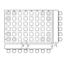
【解決手段】 LSIパッケージ1と、LSIパッケージ1の裏面にグリッド状に配置された複数の端子パッド2と、端子パッド2を介して、LSIパッケージ1を電装基板にハンダ付けするためのハンダボールとを有し、LSIパッケージ1の最外周の4角に複数配置される端子パッド群を、他の端子パッドのサイズよりも大きくした一体型の補強用パッド6として構成したBGAパッケージ
【選択図】 図4
Description
LSIパッケージと、
LSIパッケージの裏面にグリッド状に配置された複数の第1の端子パッドと、
第1の端子パッドを介して、LSIパッケージを電装基板にハンダ付けするためのハンダボールとを有し、
LSIパッケージの最外周の4角に複数配置される第1の端子パッド群を、他の第1の端子パッドのサイズよりも大きくした一体型の第1の補強用パッドとして構成したことを特徴とする。
前記第1の補強用パッドはL型パターンとして一体的に構成されている。
この第2の端子パッドは前記第1の端子パッドと前記ハンダボールを介して接続されている。
2 端子パッド
3 ハンダボール
4 電装基板
5 端子パッド
6 補強用パッド
7 ハンダボール
8 改善補強用パッド
Claims (7)
- LSIパッケージと、
LSIパッケージの裏面にグリッド状に配置された複数の第1の端子パッドと、
第1の端子パッドを介して、LSIパッケージを電装基板にハンダ付けするためのハンダボールとを有し、
LSIパッケージの最外周の4角に複数配置される第1の端子パッド群を、他の第1の端子パッドのサイズよりも大きくした一体型の第1の補強用パッドとして構成したことを特徴とするBGAパッケージ。 - 前記LSIパッケージの最外周の4角には、前記第1の端子パッドがそれぞれ少なくとも3つ配置されており、
前記第1の補強用パッドはL型パターンとして一体的に構成されていることを特徴とする請求項1に記載のBGAパッケージ。 - 前記電装基板の上面には、グリッド状に複数の第2の端子パッドが配置されており、
この第2の端子パッドは前記第1の端子パッドと前記ハンダボールを介して接続されていることを特徴とする請求項1又は2に記載のBGAパッケージ。 - 前記電装基板の最外周の4角に複数配置される第2の端子パッド群を、他の第2の端子パッドのサイズよりも大きくした一体型の第2の補強用パッドとして構成したことを特徴とする請求項1から3のいずれか1項に記載のBGAパッケージ。
- 前記第1の補強用パッドと前記第2の補強用パッドとは、前記ハンダボールよりもサイズの大きなハンダボールを介して接続されることを特徴とする請求項1から4のいずれか1項に記載のBGAパッケージ。
- 前記第1の補強用パッドと前記第2の補強用パッドとは、前記ハンダボールよりもサイズの大きなハンダボールを介して熱溶着により接続されることを特徴とする請求項5に記載のBGAパッケージ。
- 前記第2の補強用パッドはGNDに接続されることを特徴とする請求項4から6のいずれか1項に記載のBGAパッケージ。
Priority Applications (2)
| Application Number | Priority Date | Filing Date | Title |
|---|---|---|---|
| JP2008179416A JP5213034B2 (ja) | 2008-07-09 | 2008-07-09 | Bgaパッケージ |
| US12/498,137 US20100007008A1 (en) | 2008-07-09 | 2009-07-06 | Bga package |
Applications Claiming Priority (1)
| Application Number | Priority Date | Filing Date | Title |
|---|---|---|---|
| JP2008179416A JP5213034B2 (ja) | 2008-07-09 | 2008-07-09 | Bgaパッケージ |
Publications (2)
| Publication Number | Publication Date |
|---|---|
| JP2010021286A true JP2010021286A (ja) | 2010-01-28 |
| JP5213034B2 JP5213034B2 (ja) | 2013-06-19 |
Family
ID=41504425
Family Applications (1)
| Application Number | Title | Priority Date | Filing Date |
|---|---|---|---|
| JP2008179416A Expired - Fee Related JP5213034B2 (ja) | 2008-07-09 | 2008-07-09 | Bgaパッケージ |
Country Status (2)
| Country | Link |
|---|---|
| US (1) | US20100007008A1 (ja) |
| JP (1) | JP5213034B2 (ja) |
Families Citing this family (6)
| Publication number | Priority date | Publication date | Assignee | Title |
|---|---|---|---|---|
| US8766453B2 (en) | 2012-10-25 | 2014-07-01 | Freescale Semiconductor, Inc. | Packaged integrated circuit having large solder pads and method for forming |
| US10313146B2 (en) * | 2013-05-13 | 2019-06-04 | Panasonic Intellectual Property Management Co., Ltd. | Communication method and communication apparatus |
| JP6436738B2 (ja) * | 2014-11-19 | 2018-12-12 | キヤノン株式会社 | プリント配線板、半導体装置及びプリント回路板 |
| US20170269988A1 (en) * | 2016-03-21 | 2017-09-21 | Intel Corporation | Determining problem solutions based on system state data |
| US12400944B2 (en) | 2022-01-03 | 2025-08-26 | Mediatek Inc. | Board-level pad pattern for multi-row QFN packages |
| US12532758B2 (en) * | 2022-01-03 | 2026-01-20 | Mediatek Inc. | Board-level pad pattern for multi-row QFN packages |
Citations (2)
| Publication number | Priority date | Publication date | Assignee | Title |
|---|---|---|---|---|
| JP2002329812A (ja) * | 2001-04-26 | 2002-11-15 | Sharp Corp | 半導体パッケージ装置および半導体パッケージ装置実装用基板 |
| JP2007294620A (ja) * | 2006-04-24 | 2007-11-08 | Denso Corp | 半導体装置 |
Family Cites Families (3)
| Publication number | Priority date | Publication date | Assignee | Title |
|---|---|---|---|---|
| US6444563B1 (en) * | 1999-02-22 | 2002-09-03 | Motorlla, Inc. | Method and apparatus for extending fatigue life of solder joints in a semiconductor device |
| JP2007165420A (ja) * | 2005-12-12 | 2007-06-28 | Matsushita Electric Ind Co Ltd | 半導体装置 |
| US7646105B2 (en) * | 2007-11-16 | 2010-01-12 | Stats Chippac Ltd. | Integrated circuit package system with package substrate having corner contacts |
-
2008
- 2008-07-09 JP JP2008179416A patent/JP5213034B2/ja not_active Expired - Fee Related
-
2009
- 2009-07-06 US US12/498,137 patent/US20100007008A1/en not_active Abandoned
Patent Citations (2)
| Publication number | Priority date | Publication date | Assignee | Title |
|---|---|---|---|---|
| JP2002329812A (ja) * | 2001-04-26 | 2002-11-15 | Sharp Corp | 半導体パッケージ装置および半導体パッケージ装置実装用基板 |
| JP2007294620A (ja) * | 2006-04-24 | 2007-11-08 | Denso Corp | 半導体装置 |
Also Published As
| Publication number | Publication date |
|---|---|
| JP5213034B2 (ja) | 2013-06-19 |
| US20100007008A1 (en) | 2010-01-14 |
Similar Documents
| Publication | Publication Date | Title |
|---|---|---|
| CN102111957B (zh) | 用于增加每pcb层的布线通道数目的bga印迹图案 | |
| JP5107959B2 (ja) | 基板 | |
| JP5213034B2 (ja) | Bgaパッケージ | |
| JP5919558B2 (ja) | 多層プリント基板 | |
| JP2007048976A (ja) | プリント回路板、およびプリント回路板を備えた電子機器 | |
| JP2005012088A (ja) | 多層回路基板および電子機器 | |
| US6501664B1 (en) | Decoupling structure and method for printed circuit board component | |
| US8243462B2 (en) | Printed wiring board, semiconductor device, and method for manufacturing printed wiring board | |
| JP2006339316A (ja) | 半導体装置、半導体装置実装基板、および半導体装置の実装方法 | |
| US7911056B2 (en) | Substrate structure having N-SMD ball pads | |
| JP2010182792A (ja) | 電子回路装置 | |
| JP2009117409A (ja) | 回路基板 | |
| JP5691651B2 (ja) | 集積回路放熱装置及び電子装置 | |
| JP5372235B2 (ja) | 半導体装置および半導体装置実装体 | |
| JP4299087B2 (ja) | プリント配線板 | |
| JP2002151634A (ja) | 基板放熱装置 | |
| JP7423462B2 (ja) | 実装基板及び半導体装置 | |
| JP4952904B2 (ja) | プリント配線基板とこれを備えたモータ制御装置 | |
| JP6973861B2 (ja) | 半導体装置、電子機器及び半導体装置の製造方法 | |
| JP4223649B2 (ja) | プリント配線板 | |
| JP6984949B2 (ja) | 半導体装置、電子機器及び半導体装置の製造方法 | |
| JP2011129581A (ja) | プリント配線板の放熱構造 | |
| JP5691931B2 (ja) | 電子装置 | |
| JP2007123531A (ja) | プリント配線基板及びこれを用いたプリント回路基板 | |
| WO2015033509A1 (ja) | プリント配線板およびそれを備えた半導体装置 |
Legal Events
| Date | Code | Title | Description |
|---|---|---|---|
| A621 | Written request for application examination |
Free format text: JAPANESE INTERMEDIATE CODE: A621 Effective date: 20100716 |
|
| A977 | Report on retrieval |
Free format text: JAPANESE INTERMEDIATE CODE: A971007 Effective date: 20110215 |
|
| A131 | Notification of reasons for refusal |
Free format text: JAPANESE INTERMEDIATE CODE: A131 Effective date: 20120725 |
|
| A521 | Request for written amendment filed |
Free format text: JAPANESE INTERMEDIATE CODE: A523 Effective date: 20120920 |
|
| A02 | Decision of refusal |
Free format text: JAPANESE INTERMEDIATE CODE: A02 Effective date: 20121010 |
|
| A521 | Request for written amendment filed |
Free format text: JAPANESE INTERMEDIATE CODE: A523 Effective date: 20121227 |
|
| A911 | Transfer to examiner for re-examination before appeal (zenchi) |
Free format text: JAPANESE INTERMEDIATE CODE: A911 Effective date: 20130109 |
|
| TRDD | Decision of grant or rejection written | ||
| A01 | Written decision to grant a patent or to grant a registration (utility model) |
Free format text: JAPANESE INTERMEDIATE CODE: A01 Effective date: 20130130 |
|
| A61 | First payment of annual fees (during grant procedure) |
Free format text: JAPANESE INTERMEDIATE CODE: A61 Effective date: 20130220 |
|
| R150 | Certificate of patent or registration of utility model |
Ref document number: 5213034 Country of ref document: JP Free format text: JAPANESE INTERMEDIATE CODE: R150 Free format text: JAPANESE INTERMEDIATE CODE: R150 |
|
| FPAY | Renewal fee payment (event date is renewal date of database) |
Free format text: PAYMENT UNTIL: 20160308 Year of fee payment: 3 |
|
| S533 | Written request for registration of change of name |
Free format text: JAPANESE INTERMEDIATE CODE: R313533 |
|
| R350 | Written notification of registration of transfer |
Free format text: JAPANESE INTERMEDIATE CODE: R350 |
|
| LAPS | Cancellation because of no payment of annual fees |