JP2010020818A - 半導体装置及びその制御方法 - Google Patents
半導体装置及びその制御方法 Download PDFInfo
- Publication number
- JP2010020818A JP2010020818A JP2008178478A JP2008178478A JP2010020818A JP 2010020818 A JP2010020818 A JP 2010020818A JP 2008178478 A JP2008178478 A JP 2008178478A JP 2008178478 A JP2008178478 A JP 2008178478A JP 2010020818 A JP2010020818 A JP 2010020818A
- Authority
- JP
- Japan
- Prior art keywords
- time
- reference cell
- semiconductor device
- circuit
- determination
- Prior art date
- Legal status (The legal status is an assumption and is not a legal conclusion. Google has not performed a legal analysis and makes no representation as to the accuracy of the status listed.)
- Granted
Links
- 239000004065 semiconductor Substances 0.000 title claims abstract description 74
- 238000000034 method Methods 0.000 title claims description 10
- 230000008859 change Effects 0.000 claims abstract description 64
- 238000011156 evaluation Methods 0.000 claims abstract description 53
- 230000004913 activation Effects 0.000 claims description 15
- 230000007274 generation of a signal involved in cell-cell signaling Effects 0.000 claims description 4
- 230000006870 function Effects 0.000 description 34
- 238000013500 data storage Methods 0.000 description 18
- 238000010586 diagram Methods 0.000 description 17
- 239000003990 capacitor Substances 0.000 description 11
- 230000000694 effects Effects 0.000 description 10
- 238000004519 manufacturing process Methods 0.000 description 8
- 230000014759 maintenance of location Effects 0.000 description 6
- 230000008569 process Effects 0.000 description 6
- 239000007858 starting material Substances 0.000 description 3
- 239000000463 material Substances 0.000 description 2
- RYGMFSIKBFXOCR-UHFFFAOYSA-N Copper Chemical compound [Cu] RYGMFSIKBFXOCR-UHFFFAOYSA-N 0.000 description 1
- 230000003213 activating effect Effects 0.000 description 1
- 244000145845 chattering Species 0.000 description 1
- 239000004020 conductor Substances 0.000 description 1
- 229910052802 copper Inorganic materials 0.000 description 1
- 239000010949 copper Substances 0.000 description 1
- 230000007423 decrease Effects 0.000 description 1
- 238000001514 detection method Methods 0.000 description 1
- 230000006866 deterioration Effects 0.000 description 1
- 230000000415 inactivating effect Effects 0.000 description 1
- 230000007257 malfunction Effects 0.000 description 1
- 238000012986 modification Methods 0.000 description 1
- 230000004048 modification Effects 0.000 description 1
- 230000009467 reduction Effects 0.000 description 1
- 230000003068 static effect Effects 0.000 description 1
- 229910000314 transition metal oxide Inorganic materials 0.000 description 1
Images


Landscapes
- Electronic Switches (AREA)
Abstract
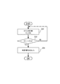
【解決手段】本発明の半導体装置は、時間経過に伴って変化する抵抗値の変化率が第1の変化率である第1参照セル44と、時間経過に伴って変化する抵抗値の変化率が第1の変化率とは異なる第2の変化率である第2参照セル46と、評価時刻における基準時刻からの第1参照セル44の抵抗値の変動量と評価時刻における基準時刻からの第2参照セル46の抵抗値の変動量との差に関係する量に基づいて、基準時刻から評価時刻までの時間が所定時間を超えるか否かを判定する判定回路48と、を具備する。
【選択図】図4
Description
ΔV=| |V1(ti)−V1(t0)|
−|V2(ti)−V2(t0)| | (1)
式(1)は以下の式(2)のように変形できる。
ΔV=| |V1(ti)−V2(ti)|
−|V1(t0)−V2(t0)| | (2)
式(2)は、評価時刻tiにおける第1参照セル44の電圧値と第2参照セル46の電圧値との差の絶対値と、第2項は基準時刻t0における第1参照セル44の電圧値と第2参照セル46の電圧値との差の絶対値との差の絶対値が、所定値ΔVとなることを意味する。
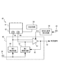
16 判定回路
18 制御回路
20 基準電圧発生回路
22 比較器
24 電源電圧
44 第1参照セル
46 第2参照セル
48 判定回路
50 第1制御回路
52 第2制御回路
54 比較器
56 電源電圧
58 設定回路
64 活性化信号発生回路
Claims (12)
- 時間経過に伴って変化する抵抗値の変化率が第1の変化率である第1の参照セルと、
時間経過に伴って変化する抵抗値の変化率が前記第1の変化率とは異なる第2の変化率である第2の参照セルと、
評価時刻における基準時刻からの前記第1の参照セルの抵抗値の変動量と評価時刻における基準時刻からの前記第2の参照セルの抵抗値の変動量との差に関係する量に基づいて、前記基準時刻から前記評価時刻までの時間が所定時間を超えるか否かを判定する判定回路と、
を具備することを特徴とする半導体装置。 - 前記第1の参照セル及び前記第2の参照セルは複数の参照セルであって、
複数の前記判定回路を有する第1の判定回路と、
前記第1の判定回路が判定した複数の判定結果のうち、前記所定時間を超えるという判定結果の個数が、所定数を超える場合に、前記基準時刻から前記評価時刻までの時間が前記所定時間を越えると判定する第2の判定回路と、
を具備することを特徴とする請求項1記載の半導体装置。 - 前記第1の参照セル及び前記第2の参照セルは抵抗変化型メモリセルであることを特徴とする請求項1または2に記載の半導体装置。
- 前記第1の参照セル及び前記第2の参照セルは相変化型メモリセルであることを特徴とする請求項1または2に記載の半導体装置。
- 前記第1の変化率と前記第2の変化率とが互いに異なるように、前記第1の参照セル及び前記第2の参照セルの抵抗値を設定する設定回路を具備することを特徴とする請求項1から4のうちいずれか一項に記載の半導体装置。
- 前記第1の参照セルの抵抗値の変動量を電圧値の変動量に変換する制御回路である第1の制御回路と、
前記第2の参照セルの抵抗値の変動量を電圧値の変動量に変換する制御回路である第2の制御回路と、
を含み、電源間で直列に接続される前記第1の参照セルと前記第1の制御回路との分圧値の変動量と、前記電源間で直列に接続される前記第2の参照セルと前記第2の制御回路との分圧値の変動量と、の差に関係する量に基づいて、前記基準時刻から前記評価時刻までの時間が所定時間を超えるか否かを判定する判定回路を具備し、
前記電源間で、前記第1の参照セル及び前記第1の制御回路と、前記第2の参照セル及び前記第2の制御回路と、が並列に接続されることを特徴とする請求項1から5のうちいずれか一項に記載の半導体装置。 - リファレンス電圧を出力する制御回路
を含み、前記リファレンス電圧の値と、電源間で直列に接続される前記第1の参照セルと前記第2の参照セルとの分圧値の変動量と、の差に関係する量に基づいて、前記基準時刻から前記評価時刻までの時間が所定時間を超えるか否かを判定する判定回路を具備することを特徴とする請求項1から5のうちいずれか一項に記載の半導体装置。 - 前記半導体装置に供給される電圧値が、前記第1の参照セル及び前記第2の参照セルが正常に動作する値に達した場合に、前記判定回路に対して活性化信号を入力する活性化信号発生回路を具備することを特徴とする請求項1から7のうちいずれか一項に記載の半導体装置。
- データを記憶するメモリセルと、
前記判定回路と接続され、前記判定回路の判定結果に基づき、前記メモリセルに記憶されたデータの消去動作を行う制御回路と、
を具備することを特徴とする請求項1から7のうちいずれか一項に記載の半導体装置。 - データを記憶するメモリセルと、
前記判定回路と接続され、前記判定回路の判定結果に基づき、前記メモリセルに対して無効なデータの書き込み動作を行う制御回路と、
を具備することを特徴とする請求項1から7のうちいずれか一項に記載の半導体装置。 - データを記憶するメモリセルと、
前記判定回路と接続され、前記判定回路の判定結果に基づき、前記メモリセルに記憶されたデータの読み出し動作を禁止する制御回路と、
を具備することを特徴とする請求項1から7のうちいずれか一項に記載の半導体装置。 - 時間経過に伴って変化する抵抗値の変化率が第1の変化率である第1の参照セルと、時間経過に伴って変化する抵抗値の変化率が前記第1の変化率とは異なる第2の変化率である第2の参照セルと、を具備する半導体装置の制御方法であって、
評価時刻における基準時刻からの前記第1の参照セルの抵抗値の変動量と評価時刻における基準時刻からの前記第2の参照セルの抵抗値の変動量との差に関係する量に基づいて、前記基準時刻から前記評価時刻までの時間が所定時間を超えるか否かを判定するステップを具備することを特徴とする半導体装置の制御方法。
Priority Applications (1)
| Application Number | Priority Date | Filing Date | Title |
|---|---|---|---|
| JP2008178478A JP5174561B2 (ja) | 2008-07-08 | 2008-07-08 | 半導体装置及びその制御方法 |
Applications Claiming Priority (1)
| Application Number | Priority Date | Filing Date | Title |
|---|---|---|---|
| JP2008178478A JP5174561B2 (ja) | 2008-07-08 | 2008-07-08 | 半導体装置及びその制御方法 |
Publications (2)
| Publication Number | Publication Date |
|---|---|
| JP2010020818A true JP2010020818A (ja) | 2010-01-28 |
| JP5174561B2 JP5174561B2 (ja) | 2013-04-03 |
Family
ID=41705559
Family Applications (1)
| Application Number | Title | Priority Date | Filing Date |
|---|---|---|---|
| JP2008178478A Expired - Fee Related JP5174561B2 (ja) | 2008-07-08 | 2008-07-08 | 半導体装置及びその制御方法 |
Country Status (1)
| Country | Link |
|---|---|
| JP (1) | JP5174561B2 (ja) |
Cited By (3)
| Publication number | Priority date | Publication date | Assignee | Title |
|---|---|---|---|---|
| US9093145B2 (en) | 2012-12-27 | 2015-07-28 | Samsung Electronics Co., Ltd. | Non-volatile random access memory device and data read method thereof |
| CN113342253A (zh) * | 2020-03-03 | 2021-09-03 | 江苏时代全芯存储科技股份有限公司 | 混合型存储器 |
| CN113628652A (zh) * | 2020-05-08 | 2021-11-09 | 华邦电子股份有限公司 | 电阻式存储装置及其写入电压的调整方法 |
Citations (2)
| Publication number | Priority date | Publication date | Assignee | Title |
|---|---|---|---|---|
| JPS5545250A (en) * | 1978-09-26 | 1980-03-29 | Toshiba Corp | Timer circuit |
| JPH01268312A (ja) * | 1988-04-20 | 1989-10-26 | Matsushita Electric Ind Co Ltd | タイマ回路 |
-
2008
- 2008-07-08 JP JP2008178478A patent/JP5174561B2/ja not_active Expired - Fee Related
Patent Citations (2)
| Publication number | Priority date | Publication date | Assignee | Title |
|---|---|---|---|---|
| JPS5545250A (en) * | 1978-09-26 | 1980-03-29 | Toshiba Corp | Timer circuit |
| JPH01268312A (ja) * | 1988-04-20 | 1989-10-26 | Matsushita Electric Ind Co Ltd | タイマ回路 |
Cited By (4)
| Publication number | Priority date | Publication date | Assignee | Title |
|---|---|---|---|---|
| US9093145B2 (en) | 2012-12-27 | 2015-07-28 | Samsung Electronics Co., Ltd. | Non-volatile random access memory device and data read method thereof |
| CN113342253A (zh) * | 2020-03-03 | 2021-09-03 | 江苏时代全芯存储科技股份有限公司 | 混合型存储器 |
| CN113628652A (zh) * | 2020-05-08 | 2021-11-09 | 华邦电子股份有限公司 | 电阻式存储装置及其写入电压的调整方法 |
| CN113628652B (zh) * | 2020-05-08 | 2024-01-23 | 华邦电子股份有限公司 | 电阻式存储装置及其写入电压的调整方法 |
Also Published As
| Publication number | Publication date |
|---|---|
| JP5174561B2 (ja) | 2013-04-03 |
Similar Documents
| Publication | Publication Date | Title |
|---|---|---|
| US7630266B2 (en) | Temperature compensation of memory signals using digital signals | |
| US7630265B2 (en) | On-chip temperature sensor | |
| KR100859257B1 (ko) | 메모리 | |
| US8400824B2 (en) | Non-volatile memory device and method for controlling the same | |
| US20110222355A1 (en) | Control voltage generation circuit and nonvolatile storage device having the same | |
| US10297317B2 (en) | Non-volatile semiconductor memory device including clamp circuit with control transistor and amplifier circuit | |
| JP6336541B2 (ja) | センス増幅器のためのトリミング可能な基準発生器 | |
| JP3688899B2 (ja) | 半導体集積回路装置 | |
| KR20120063165A (ko) | 반도체 장치 및 상기 반도체 장치의 데이터 감지 방법 | |
| JP2009020998A (ja) | 読み出しエラーを減らすことができるマルチレベル相変化メモリ装置及びその読み出し方法 | |
| US9019746B2 (en) | Resistive memory device and method for driving the same | |
| KR100420125B1 (ko) | 비휘발성 반도체 메모리 장치와 그것의 파워-업 독출 방법 | |
| KR20140080945A (ko) | 비휘발성 메모리 장치 | |
| US20100290278A1 (en) | Semiconductor memory device rewriting data after execution of multiple read operations | |
| JP5406920B2 (ja) | 不揮発性メモリ基準セルの電気的なトリミングの方法 | |
| CN110120239B (zh) | 半导体存储器装置 | |
| CN111933208B (zh) | 半导体存储装置 | |
| US7075844B2 (en) | Parallel sense amplifier with mirroring of the current to be measured into each reference branch | |
| JP5174561B2 (ja) | 半導体装置及びその制御方法 | |
| KR102444408B1 (ko) | 반도체 장치 | |
| US20050111261A1 (en) | Non-volatile semiconductor memory device having sense amplifier with increased speed | |
| JP5160780B2 (ja) | フラッシュメモリ装置の電圧生成器 | |
| US7512026B2 (en) | Sense amplifying circuit capable of operating with lower voltage and nonvolatile memory device including the same | |
| JP5250254B2 (ja) | 不揮発性半導体メモリ装置 | |
| US20210286562A1 (en) | Write method for resistive memory |
Legal Events
| Date | Code | Title | Description |
|---|---|---|---|
| RD04 | Notification of resignation of power of attorney |
Free format text: JAPANESE INTERMEDIATE CODE: A7424 Effective date: 20100402 |
|
| RD03 | Notification of appointment of power of attorney |
Free format text: JAPANESE INTERMEDIATE CODE: A7423 Effective date: 20100616 |
|
| A621 | Written request for application examination |
Free format text: JAPANESE INTERMEDIATE CODE: A621 Effective date: 20110701 |
|
| RD03 | Notification of appointment of power of attorney |
Free format text: JAPANESE INTERMEDIATE CODE: A7423 Effective date: 20120830 |
|
| A977 | Report on retrieval |
Free format text: JAPANESE INTERMEDIATE CODE: A971007 Effective date: 20121130 |
|
| TRDD | Decision of grant or rejection written | ||
| A01 | Written decision to grant a patent or to grant a registration (utility model) |
Free format text: JAPANESE INTERMEDIATE CODE: A01 Effective date: 20121205 |
|
| A61 | First payment of annual fees (during grant procedure) |
Free format text: JAPANESE INTERMEDIATE CODE: A61 Effective date: 20121228 |
|
| R150 | Certificate of patent or registration of utility model |
Ref document number: 5174561 Country of ref document: JP Free format text: JAPANESE INTERMEDIATE CODE: R150 |
|
| S111 | Request for change of ownership or part of ownership |
Free format text: JAPANESE INTERMEDIATE CODE: R313111 |
|
| R350 | Written notification of registration of transfer |
Free format text: JAPANESE INTERMEDIATE CODE: R350 |
|
| R250 | Receipt of annual fees |
Free format text: JAPANESE INTERMEDIATE CODE: R250 |
|
| R250 | Receipt of annual fees |
Free format text: JAPANESE INTERMEDIATE CODE: R250 |
|
| R250 | Receipt of annual fees |
Free format text: JAPANESE INTERMEDIATE CODE: R250 |
|
| LAPS | Cancellation because of no payment of annual fees |