JP2010020818A - Semiconductor device and method of controlling the same - Google Patents
Semiconductor device and method of controlling the same Download PDFInfo
- Publication number
- JP2010020818A JP2010020818A JP2008178478A JP2008178478A JP2010020818A JP 2010020818 A JP2010020818 A JP 2010020818A JP 2008178478 A JP2008178478 A JP 2008178478A JP 2008178478 A JP2008178478 A JP 2008178478A JP 2010020818 A JP2010020818 A JP 2010020818A
- Authority
- JP
- Japan
- Prior art keywords
- time
- reference cell
- semiconductor device
- circuit
- determination
- Prior art date
- Legal status (The legal status is an assumption and is not a legal conclusion. Google has not performed a legal analysis and makes no representation as to the accuracy of the status listed.)
- Granted
Links
Images


Landscapes
- Electronic Switches (AREA)
Abstract
Description
本発明は、可変抵抗を有する半導体装置に関する。 The present invention relates to a semiconductor device having a variable resistor.
半導体装置に用いられるデータ記憶素子には、DRAM(Dynamic Random Access Memory)やSRAM(Static Random Access Memory)等の揮発性のデータ記憶素子と、フラッシュメモリやEEPROM(Electrically Erasable and Programmable Read Only Memory)等の不揮発性のデータ記憶素子がある。揮発性のデータ記憶素子は、データの書き込み及び読み出しを高速に行うことができるが、データの保持性に乏しい。不揮発性のデータ記憶素子は、データの保持性に優れる反面、書き込み・読み出し速度が揮発性のデータ記憶素子に比べて遅い。 Data storage elements used in semiconductor devices include volatile data storage elements such as DRAM (Dynamic Random Access Memory) and SRAM (Static Random Access Memory), flash memory and EEPROM (Electrically Erasable and Programmable Read Only Memory), etc. There are non-volatile data storage elements. Volatile data storage elements can write and read data at high speed, but have poor data retention. A nonvolatile data storage element is excellent in data retention, but has a slower writing / reading speed than a volatile data storage element.
一方、ReRAM(Resistance Random Access Memory)やPRAM(Phase change Random Access Memory)等の可変抵抗の抵抗率によりデータを記憶するデータ記憶素子が開発されている。可変抵抗を有するデータ記憶素子は、可変抵抗を高抵抗状態及び低抵抗状態のうちいずれかに変化させてデータを記憶する。可変抵抗を有するデータ記憶素子のデータの保持性は、揮発性のデータ記憶素子と不揮発性のデータ記憶素子との中間の性能であり、時間または日単位程度である。例えば、特許文献1、特許文献2、及び、特許文献3には、プログラム可能な抵抗素子付きメモリを使用した半導体装置が示されている。 On the other hand, data storage elements that store data by the resistivity of variable resistors such as ReRAM (Resistance Random Access Memory) and PRAM (Phase change Random Access Memory) have been developed. A data storage element having a variable resistance stores data by changing the variable resistance to either a high resistance state or a low resistance state. Data retention of a data storage element having a variable resistance is an intermediate performance between a volatile data storage element and a non-volatile data storage element, and is on the order of hours or days. For example, Patent Document 1, Patent Document 2, and Patent Document 3 show semiconductor devices using a memory with a programmable resistance element.
可変抵抗の抵抗値は、時間経過に伴って変動する。抵抗値の変動量を利用して、所定時間が経過したことを判定するタイマー機能を実現できる。可変抵抗を有する半導体装置のタイマー機能の精度がばらつくという課題があった。 The resistance value of the variable resistor varies with time. A timer function for determining that a predetermined time has elapsed can be realized using the variation amount of the resistance value. There is a problem that the accuracy of the timer function of the semiconductor device having a variable resistor varies.
本発明は、上記課題に鑑みなされたものであり、可変抵抗を有する半導体装置のタイマー機能の精度のばらつきを低減することを目的とする。 The present invention has been made in view of the above problems, and an object thereof is to reduce variation in accuracy of a timer function of a semiconductor device having a variable resistor.
本発明は、時間経過に伴って変化する抵抗値の変化率が第1の変化率である第1の参照セルと、時間経過に伴って変化する抵抗値の変化率が前記第1の変化率とは異なる第2の変化率である第2の参照セルと、評価時刻における基準時刻からの前記第1の参照セルの抵抗値の変動量と評価時刻における基準時刻からの前記第2の参照セルの抵抗値の変動量との差に関係する量に基づいて、前記基準時刻から前記評価時刻までの時間が所定時間を越えるか否かを判定する判定回路と、を具備することを特徴とする半導体装置である。本発明によれば、1つの参照セルの抵抗値の変動量ではなく、第1の参照セルの抵抗値の変動量と第2の参照セルの抵抗値の変動量との差に関係する相対的な量に基づいて、所定時間が経過したことを判定することができる。したがって、可変抵抗を有する参照セルの製造プロセスや動作させる温度環境の違いの影響による抵抗値の変動を抑えることができる。ゆえに、可変抵抗を有する半導体装置のタイマー機能の精度のばらつきの低減に効果がある。 The present invention provides a first reference cell having a first rate of change in resistance value that changes with time, and a first rate of change in resistance value that changes with time. A second reference cell having a second rate of change different from the first reference cell, and a variation amount of the resistance value of the first reference cell from the reference time at the evaluation time and the second reference cell from the reference time at the evaluation time A determination circuit for determining whether or not a time from the reference time to the evaluation time exceeds a predetermined time based on an amount related to a difference between the resistance value variation amount of the first resistance value and the evaluation value. It is a semiconductor device. According to the present invention, not the amount of variation in the resistance value of one reference cell, but the relative amount related to the difference between the amount of variation in the resistance value of the first reference cell and the amount of variation in the resistance value of the second reference cell. Based on the correct amount, it can be determined that the predetermined time has elapsed. Therefore, it is possible to suppress the variation of the resistance value due to the influence of the difference in the manufacturing process of the reference cell having the variable resistance and the operating temperature environment. Therefore, there is an effect in reducing variation in accuracy of the timer function of the semiconductor device having a variable resistor.
上記構成において、前記第1の参照セル及び前記第2の参照セルは複数の参照セルであって、複数の前記判定回路を有する第1の判定回路と、前記第1の判定回路が判定した複数の判定結果のうち、前記所定時間を超えるという判定結果の個数が、所定数を超える場合に、前記基準時刻から前記評価時刻までの時間が前記所定時間を越えると判定する第2の判定回路を具備する構成とすることができる。この構成によれば、複数の可変抵抗を有する参照セル間の精度のばらつきを抑えることができる。したがって、可変抵抗を有する半導体装置のタイマー機能の精度のばらつきの低減に効果がある。 In the above configuration, the first reference cell and the second reference cell are a plurality of reference cells, and a first determination circuit having a plurality of the determination circuits and a plurality of determinations determined by the first determination circuit A second determination circuit that determines that the time from the reference time to the evaluation time exceeds the predetermined time when the number of determination results that exceed the predetermined time exceeds the predetermined time It can be set as the structure to comprise. According to this configuration, variation in accuracy between reference cells having a plurality of variable resistors can be suppressed. Therefore, there is an effect in reducing variation in accuracy of the timer function of the semiconductor device having a variable resistor.
上記構成において、前記第1の参照セル及び前記第2の参照セルは抵抗変化型メモリセルである構成とすることができる。 In the above configuration, the first reference cell and the second reference cell may be variable resistance memory cells.
上記構成において、前記第1の参照セル及び前記第2の参照セルは相変化型メモリセルである構成とすることができる。 In the above configuration, the first reference cell and the second reference cell may be phase change type memory cells.
上記構成において、前記第1の変化率と前記第2の変化率とが互いに異なるように、前記第1の参照セル及び前記第2の参照セルの抵抗値を設定する設定回路を具備する構成とすることができる。 In the configuration described above, a configuration is provided that includes a setting circuit that sets resistance values of the first reference cell and the second reference cell so that the first change rate and the second change rate are different from each other. can do.
上記構成において、前記第1の参照セルの抵抗値の変動量を電圧値の変動量に変換する制御回路である第1の制御回路と、前記第2の参照セルの抵抗値の変動量を電圧値の変動量に変換する制御回路である第2の制御回路と、を含み、電源間で直列に接続される前記第1の参照セルと前記第1の制御回路との分圧値の変動量と、前記電源間で直列に接続される前記第2の参照セルと前記第2の制御回路との分圧値の変動量と、の差に関係する量に基づいて、前記基準時刻から前記評価時刻までの時間が所定時間を超えるか否かを判定する判定回路を具備し、前記電源間で、前記第1の参照セル及び前記第1の制御回路と、前記第2の参照セル及び前記第2の制御回路と、が並列に接続される構成とすることができる。 In the above configuration, the first control circuit, which is a control circuit that converts the fluctuation amount of the resistance value of the first reference cell into the fluctuation amount of the voltage value, and the fluctuation amount of the resistance value of the second reference cell are the voltage. A second control circuit that is a control circuit that converts the value into a fluctuation amount of the value, and a fluctuation amount of a divided value between the first reference cell and the first control circuit that are connected in series between the power supplies And the evaluation from the reference time based on the amount related to the difference between the second reference cell connected in series between the power supplies and the amount of variation in the divided voltage value of the second control circuit. A determination circuit for determining whether or not a time until a time exceeds a predetermined time, and the first reference cell, the first control circuit, the second reference cell, and the first between the power sources Two control circuits can be connected in parallel.
上記構成において、リファレンス電圧を出力する制御回路を含み、前記リファレンス電圧の値と、電源間で直列に接続される前記第1の参照セルと前記第2の参照セルとの分圧値の変動量と、の差に関係する量に基づいて、前記基準時刻から前記評価時刻までの時間が所定時間を超えるか否かを判定する判定回路を具備する構成とすることができる。 The above configuration includes a control circuit that outputs a reference voltage, and the amount of change in the value of the reference voltage and the divided value of the first reference cell and the second reference cell connected in series between the power supplies And a determination circuit that determines whether or not the time from the reference time to the evaluation time exceeds a predetermined time based on an amount related to the difference between the reference time and the evaluation time.
上記構成において、前記半導体装置に供給される電圧値が、前記第1の参照セル及び前記第2の参照セルが正常に動作する値に達した場合に、前記判定回路に対して活性化信号を入力する活性化信号発生回路を具備する構成とすることができる。この構成によれば、半導体装置に供給される電圧値が、参照セルが正常に動作する値に達するまでの間、判定回路を非活性とすることにより、判定回路の誤動作を防止することができる。したがって、可変抵抗を有する半導体装置のタイマー機能の精度の向上に効果がある。 In the above configuration, when a voltage value supplied to the semiconductor device reaches a value at which the first reference cell and the second reference cell operate normally, an activation signal is sent to the determination circuit. An activation signal generating circuit for inputting may be provided. According to this configuration, the malfunction of the determination circuit can be prevented by deactivating the determination circuit until the voltage value supplied to the semiconductor device reaches a value at which the reference cell operates normally. . Therefore, there is an effect in improving the accuracy of the timer function of the semiconductor device having a variable resistor.
上記構成において、データを記憶するメモリセルと、前記判定回路と接続され、前記判定回路の判定結果に基づき、前記メモリセルに記憶されたデータの消去動作を行う制御回路と、を具備する構成とすることができる。この構成によれば、タイマー機能の精度のばらつきを低減した判定回路により所定時間が経過したことを精度よく判定して、制御回路がメモリセルに記憶されたデータの消去動作を行うことができる。したがって、可変抵抗を有する半導体装置のセキュリティの向上に効果がある。 In the above configuration, a configuration includes: a memory cell that stores data; and a control circuit that is connected to the determination circuit and performs an erasing operation of data stored in the memory cell based on a determination result of the determination circuit; can do. According to this configuration, it is possible to accurately determine that the predetermined time has elapsed by the determination circuit that reduces the variation in accuracy of the timer function, and the control circuit can perform the erasing operation of the data stored in the memory cell. Therefore, there is an effect in improving the security of the semiconductor device having a variable resistance.
上記構成において、データを記憶するメモリセルと、前記判定回路と接続され、前記判定回路の判定結果に基づき、前記メモリセルに対して無効なデータの書き込み動作を行う制御回路と、を具備する構成とすることができる。この構成によれば、タイマー機能の精度のばらつきを低減した判定回路により所定時間が経過したことを精度よく判定して、制御回路がメモリセルへの無効なデータの書き込み動作を行うことができる。したがって、可変抵抗を有する半導体装置のセキュリティの向上に効果がある。 In the above configuration, a configuration includes: a memory cell that stores data; and a control circuit that is connected to the determination circuit and performs an invalid data write operation on the memory cell based on a determination result of the determination circuit. It can be. According to this configuration, it is possible to accurately determine that the predetermined time has elapsed by the determination circuit that reduces the variation in accuracy of the timer function, and the control circuit can perform an invalid data write operation to the memory cell. Therefore, there is an effect in improving the security of the semiconductor device having a variable resistance.
上記構成において、データを記憶するメモリセルと、前記判定回路と接続され、前記判定回路の判定結果に基づき、前記メモリセルに記憶されたデータの読み出し動作を禁止する制御回路と、を具備する構成とすることができる。この構成によれば、タイマー機能の精度のばらつきを低減した判定回路により所定時間が経過したことを精度よく判定して、制御回路がメモリセルに記憶されたデータの読み出しの禁止動作を行うことができる。したがって、可変抵抗を有する半導体装置のセキュリティの向上に効果がある。 In the above configuration, a configuration includes: a memory cell that stores data; and a control circuit that is connected to the determination circuit and prohibits a read operation of data stored in the memory cell based on a determination result of the determination circuit. It can be. According to this configuration, it is possible to accurately determine that the predetermined time has elapsed by the determination circuit that reduces the variation in accuracy of the timer function, and the control circuit performs an operation of prohibiting reading of data stored in the memory cell. it can. Therefore, there is an effect in improving the security of the semiconductor device having a variable resistance.
本発明は、時間経過に伴って変化する抵抗値の変化率が第1の変化率である第1の参照セルと、時間経過に伴って変化する抵抗値の変化率が前記第1の変化率とは異なる第2の変化率である第2の参照セルと、を具備する半導体装置の制御方法であって、評価時刻における基準時刻からの前記第1の参照セルの抵抗値の変動量と評価時刻における基準時刻からの前記第2の参照セルの抵抗値の変動量との差に関係する量に基づいて、前記基準時刻から前記評価時刻までの時間が所定時間を超えるか否かを判定するステップを具備することを特徴とする半導体装置の制御方法である。本発明によれば、1つの参照セルの抵抗値の変動量ではなく、第1の参照セルの抵抗値の変動量と第2の参照セルの抵抗値の変動量との差に関係する相対的な量に基づいて、所定時間が経過したことを判定することができる。したがって、可変抵抗を有する参照セルの製造プロセスや動作させる温度環境の違いの影響による抵抗値の変動を抑えることができる。ゆえに、可変抵抗を有する半導体装置のタイマー機能の精度のばらつきの低減に効果がある。 The present invention provides a first reference cell having a first rate of change in resistance value that changes with time, and a first rate of change in resistance value that changes with time. And a second reference cell having a second rate of change different from that of the first reference cell, the variation amount of the resistance value of the first reference cell from the reference time at the evaluation time and the evaluation It is determined whether or not the time from the reference time to the evaluation time exceeds a predetermined time based on an amount related to a difference between the resistance value variation amount of the second reference cell from the reference time at the time A method of controlling a semiconductor device comprising steps. According to the present invention, not the amount of variation in the resistance value of one reference cell, but the relative amount related to the difference between the amount of variation in the resistance value of the first reference cell and the amount of variation in the resistance value of the second reference cell. Based on the correct amount, it can be determined that the predetermined time has elapsed. Therefore, it is possible to suppress the variation of the resistance value due to the influence of the difference in the manufacturing process of the reference cell having the variable resistance and the operating temperature environment. Therefore, there is an effect in reducing variation in accuracy of the timer function of the semiconductor device having a variable resistor.
本発明によれば、可変抵抗を有する参照セルの製造プロセスや動作させる温度環境の違いの影響による抵抗値の変動を抑えることができるため、可変抵抗を有する半導体装置のタイマー機能の精度のばらつきの低減に効果がある。 According to the present invention, it is possible to suppress variations in the resistance value due to the difference in the manufacturing process of the reference cell having a variable resistor and the operating temperature environment, so that the variation in the accuracy of the timer function of the semiconductor device having the variable resistor can be reduced. It is effective for reduction.
本発明の実施例との比較のため、図1、図2及び図3を参照に、可変抵抗を有する半導体装置の構成ならびにタイマー機能の動作の一例を説明する。 For comparison with the embodiment of the present invention, an example of a configuration of a semiconductor device having a variable resistor and an operation of a timer function will be described with reference to FIGS. 1, 2, and 3. FIG.
図1を参照に、半導体装置の構成を説明する。図1は、半導体装置10の構成を示すブロック図である。メモリセルアレイ11は、データ記憶素子を有する。参照セル部12は、可変抵抗を有する参照セル14を有する。判定回路16は、制御回路18、基準電圧発生回路20及び比較器22を有する。制御回路18及び基準電圧発生回路20には、電圧Vcc24が印加される。参照セル14と制御回路18とは直列に接続される。参照セル14の抵抗値は、制御回路18により電圧値に変換される。評価時刻tにおける参照セル14の電圧値をV(t)とする。基準電圧発生回路20は、基準電圧Vrefを発生する。
The structure of the semiconductor device will be described with reference to FIG. FIG. 1 is a block diagram showing a configuration of the
基準時刻をt0、所定時間をTi、及び、基準時刻t0から所定時間Tiが経過した評価時刻をtiとする。設定回路26は、参照セル14の電圧値V(t)が、時間経過に伴って低下して、評価時刻tが基準時刻t0から所定時間Tiを経過した後、基準電圧Vrefの値よりも小さくなるように、参照セル14の抵抗値を設定する。
The reference time is t0, the predetermined time is Ti, and the evaluation time when the predetermined time Ti has elapsed from the reference time t0 is ti. In the
図2及び図3を参照に、半導体装置が有するタイマー機能の動作を説明する。図2は、評価時刻tに対する電圧値V(t)の変化を示すグラフである。電圧値V(t0)、V(ti)は、それぞれ、基準時刻t0、評価時刻tiにおける電圧値を示す。V(ti)は基準電圧Vrefの値と一致する。 The operation of the timer function of the semiconductor device is described with reference to FIGS. FIG. 2 is a graph showing changes in the voltage value V (t) with respect to the evaluation time t. The voltage values V (t0) and V (ti) indicate voltage values at the reference time t0 and the evaluation time ti, respectively. V (ti) matches the value of the reference voltage Vref.
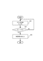
図3は、評価時刻tにおける判定回路16のタイマー機能の動作を示すフローチャートである。まず、評価時刻tにおける電圧値V(t)を計測する(ステップS30)。評価時刻tの初期値は、基準時刻t0である。比較器22において、電圧値V(t)と基準電圧Vrefの値を比較する(ステップS32)。電圧値V(t)が基準電圧Vrefの値より小さい場合(ステップS32のYES)、基準時刻t0から所定時間Tiが経過したことを意味するので、比較器22は判定信号28を出力する(ステップS34)。電圧値V(t)が基準電圧Vrefの値より小さい場合とは、図2において、評価時刻tが評価時刻tiより大きい場合に対応する。電圧値V(t)が基準電圧Vrefの値以上である場合(ステップS32のNO)、ステップS30からの処理を繰り返す。電圧値V(t)が基準電圧Vrefの値以上である場合とは、図2において、評価時刻tがt0以上ti以下の場合に対応する。以上が、半導体装置10のタイマー機能の説明である。
FIG. 3 is a flowchart showing the operation of the timer function of the
しかしながら、可変抵抗の抵抗値の変動量は、可変抵抗の製造プロセスや動作させる温度環境の影響のため、ばらついてしまう。そのため、可変抵抗を有する参照セルを使用した半導体装置のタイマー機能の精度がばらつくという課題があった。例えば、一方の半導体装置では、所定時間を超過した後に所定時間と判定されるが、他方の半導体装置では、タイマー機能を開始した途端に所定時間と判定されるという課題があった。 However, the fluctuation amount of the resistance value of the variable resistor varies due to the influence of the variable resistor manufacturing process and the operating temperature environment. Therefore, there is a problem that the accuracy of the timer function of the semiconductor device using the reference cell having the variable resistance varies. For example, in one semiconductor device, the predetermined time is determined after a predetermined time is exceeded, but in the other semiconductor device, the predetermined time is determined as soon as the timer function is started.
以下、図4、図5、図6及び図7を参照に、本発明の実施例である、可変抵抗を有し、タイマー機能の精度のばらつきを低減した半導体装置の実施例について説明する。 Hereinafter, with reference to FIGS. 4, 5, 6, and 7, an embodiment of the semiconductor device having a variable resistor and having reduced variation in accuracy of the timer function, which is an embodiment of the present invention, will be described.
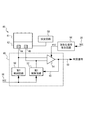
図4は、半導体装置40の構成を示すブロック図である。メモリセルアレイ41は、データ記憶素子を有する。参照セル部42は、可変抵抗を有する第1参照セル44及び第2参照セル46を有する。判定回路48は、第1制御回路50、第2制御回路52及び比較器54を有する。第1制御回路50及び第2制御回路52には、電圧Vcc56が印加される。直列に接続された第1参照セル44及び第1制御回路50と、直列に接続された第2参照セル46及び第2制御回路52とは並列に接続される。第1参照セル44、第2参照セル46の抵抗値は、それぞれ第1制御回路50、第2制御回路52により電圧値に変換される。第1制御回路50が、評価時刻tにおける第1参照セル44の抵抗値を変換した電圧値をV1(t)とする。第2制御回路52が、評価時刻tにおける第2参照セル46の抵抗値を変換した電圧値をV2(t)とする。比較器54は、電圧値V1(t)及び電圧値V2(t)を入力とし、電圧値V1(t)と電圧値V2(t)との差に基づく量と所定値の比較結果に基づいて、判定信号60を出力する。
FIG. 4 is a block diagram showing a configuration of the
活性化信号発生回路64は、入力される電圧Vcc56が所定値に達した場合に、活性化信号enzを比較器54に対して出力する。所定値とは、例えば、メモリセルアレイ41及び参照セル部42の正常な動作が保障される電圧値である。比較器54は、活性化信号enzが入力されると活性化され、電圧値V1(t)と電圧値V2(t)との比較を行うことができるようになる。
The activation
比較器54の出力である判定信号60は、比較器54にヒステリシスを持たせるため、信号線62により、第2制御回路52へフィードバックされる。これにより、比較器54が入力信号のわずかな差やノイズ混入を検出した場合に、判定信号60のチャタリングを防止できる。
The
基準時刻をt0、所定時間をTi、基準時刻t0から所定時間Tiが経過した評価時刻をti、及び、所定値をΔVとする。設定回路58は、電圧値V1(t)の変化率と電圧値V2(t)の変化率とが互いに異なるように、第1参照セル44及び第2参照セル46の抵抗値を設定する。また、設定回路58は、評価時刻tiにおける基準時刻t0からの第1参照セル44の電圧値の変動量の絶対値と、評価時刻tiにおける基準時刻t0からの第2参照セル46の電圧値の変動量の絶対値との差の絶対値が、所定値ΔVとなるように、第1参照セル44及び第2参照セル46の抵抗値を設定する。すなわち、以下の式(1)が成立する。
ΔV=| |V1(ti)−V1(t0)|
−|V2(ti)−V2(t0)| | (1)
式(1)は以下の式(2)のように変形できる。
ΔV=| |V1(ti)−V2(ti)|
−|V1(t0)−V2(t0)| | (2)
式(2)は、評価時刻tiにおける第1参照セル44の電圧値と第2参照セル46の電圧値との差の絶対値と、第2項は基準時刻t0における第1参照セル44の電圧値と第2参照セル46の電圧値との差の絶対値との差の絶対値が、所定値ΔVとなることを意味する。
The reference time is t0, the predetermined time is Ti, the evaluation time when the predetermined time Ti has elapsed from the reference time t0 is ti, and the predetermined value is ΔV. The setting
ΔV = || V1 (ti) −V1 (t0) |
− | V2 (ti) −V2 (t0) || (1)
Expression (1) can be transformed as the following expression (2).
ΔV = || V1 (ti) −V2 (ti) |
− | V1 (t0) −V2 (t0) || (2)
Equation (2) is the absolute value of the difference between the voltage value of the
図5は、評価時刻tに対する電圧値V1(t)及び電圧値V2(t)の変化を示すグラフである。電圧値V1(t0)、V1(ti)は、それぞれ、基準時刻t0、評価時刻tiにおける第1参照セル44の電圧値を示す。電圧値V2(t0)、V2(ti)は、それぞれ、基準時刻t0、評価時刻tiにおける第2参照セル46の電圧値を示す。電圧値V1(t)、V2(t)のグラフの傾きは、それぞれ電圧値V1(t)、V2(t)の変化率を示し、電圧値V1(t)の変化率と電圧値V2(t)の変化率とが互いに異なることを示している。
FIG. 5 is a graph showing changes in the voltage value V1 (t) and the voltage value V2 (t) with respect to the evaluation time t. The voltage values V1 (t0) and V1 (ti) indicate the voltage values of the
図6は、判定回路48のタイマー機能の動作を示すフローチャートである。まず、基準時刻t0における電圧値V1(t0)及びV2(t0)を計測する(ステップS70)。電圧値V1(t0)とV2(t0)との差の絶対値|V1(t0)−V2(t0)|を変数αに格納する(ステップS72)。評価時刻tにおける電圧値V1(t)及びV2(t)を計測する(ステップS74)。電圧値V1(t)と電圧値V2(t)との差の絶対値|V1(t)−V2(t)|を変数βに格納する(ステップS76)。変数αと変数βとの差の絶対値|α−β|が所定値ΔVを超えるか否かを確認する(ステップS78)。|α−β|が所定値ΔVを超える場合(ステップS78のYES)、基準時刻t0から所定時間Tiが経過したことを意味するので、比較器54は判定信号60を出力する(ステップS78)。|α−β|が所定値ΔV以下である場合(ステップS80のNO)、ステップS74からの処理を繰り返す。以上により、基準時刻t0から所定時間Tiが経過したことを判定するタイマー機能を実現することができる。
FIG. 6 is a flowchart showing the operation of the timer function of the
図7は、図4の第1参照セル44及び第2参照セル46に対応する参照セル82の構成を示す断面図である。参照セル82は、可変抵抗84及びその両端に設けられた電極86から構成される。可変抵抗84は、抵抗値の大小によりデータを記憶するもので、電流が流れることにより抵抗値が大きく(例えば104倍以上)変化する物質からなる。このような物質には、例えばCuOをはじめとする遷移金属酸化物がある。電極86は、容量として電荷を蓄えることによりデータを記憶するもので、例えば銅などの伝導性の高い物質からなる。可変抵抗84の周囲は、絶縁部88にて覆われている。
FIG. 7 is a cross-sectional view showing the configuration of the
実施例1において、時間経過に伴って変化する抵抗値の変化率が第1の変化率である第1参照セル44と、時間経過に伴って変化する抵抗値の変化率が前記第1の変化率とは異なる第2の変化率である第2参照セル46と、評価時刻tにおける基準時刻t0からの第1参照セル44の抵抗値の変動量と評価時刻tにおける基準時刻t0からの第2参照セル46の抵抗値の変動量との差に関係する量に基づいて、基準時刻t0から評価時刻tまでの時間が所定時間Tiを超えるか否かを判定する判定回路48と、を具備する構成とする一例を説明した。この構成によれば、1つの参照セルの抵抗値の変動量ではなく、第1の参照セルの抵抗値の変動量と第2の参照セルの抵抗値の変動量との差に関係する相対的な量に基づいて、所定時間が経過したことを判定することができる。したがって、参照セルの製造プロセスや参照セルを動作させる温度環境の違いの影響による変動を抑えることができる。ゆえに、半導体装置のタイマー機能の精度のばらつきの低減に効果がある。
In the first embodiment, the
実施例1において、第1参照セル44及び第2参照セル46は、抵抗変化型メモリセル及び相変化型メモリセルのいずれであってもよい。
In the first embodiment, the
実施例1において、第1参照セル44及び第2参照セル46と、メモリセルアレイ41が有するデータ記憶素子とを、同じ構成としてもよい。また、第1参照セル44及び第2参照セル46はメモリセルアレイ41の中に配置されてもよい。これにより、参照セルとメモリセルアレイが有するデータ記憶素子とを同じ製造方法により製造できるため、コストの低減に効果がある。
In the first embodiment, the
実施例1において、設定回路58は、V1(t)の変化率とV2(t)の変化率とが互いに異なるように、第1参照セル44及び第2参照セル46の抵抗値を設定する。V1(t)の変化率とV2(t)の変化率とが互いに異なるように、設定回路58は、第1参照セル44及び第2参照セル46に対して、電圧を印加する時間を異ならせてもよいし、また、印加する電流の大きさを異ならせてもよい。
In the first embodiment, the setting
実施例1において、半導体装置に供給される電圧Vcc56が、第1参照セル44及び第2参照セル46が正常に動作する値に達した場合に、判定回路48に対して活性化信号enzを入力する活性化信号発生回路64を具備する構成とする一例を説明した。この構成によれば、半導体装置に供給される電圧が、参照セルが正常に動作する値に達するまでの間、判定回路を非活性とすることにより、判定回路の誤動作を防止することができる。したがって、可変抵抗を有する半導体装置のタイマー機能の精度の向上に効果がある。
In the first embodiment, when the
以下、図8を参照に、複数の参照セルと複数の判定回路とによる複数の判定結果を用いて、所定時間が経過したことを判定する判定回路を使用した、タイマー機能を備えた半導体装置の実施例について説明する。図8は、5つの参照セルと4つの判定回路とによる4つの判定結果を用いて、所定時間が経過したことを判定する判定回路を使用した、タイマー機能を備えた半導体装置の構成を示すブロック図である。メモリセルアレイ90は、データ記憶素子を有する。参照セル部92は、可変抵抗を有する第1〜第5の参照セル94〜102を有する。第1判定回路104は、制御回路106、第1〜第4の比較器108〜114を有する。制御回路106には、電圧Vcc116が印加される。制御回路106は、第1〜第5の参照セル94〜102の抵抗値を電圧値に変換する。
Hereinafter, referring to FIG. 8, a semiconductor device having a timer function using a determination circuit that determines that a predetermined time has elapsed by using a plurality of determination results by a plurality of reference cells and a plurality of determination circuits. Examples will be described. FIG. 8 is a block diagram illustrating a configuration of a semiconductor device having a timer function using a determination circuit that determines that a predetermined time has elapsed using four determination results of five reference cells and four determination circuits. FIG. The
第1〜第4の比較器108〜114は、それぞれ、第1参照セル94と第2参照セル96、第1参照セル94と第3参照セル98、第1参照セル94と第4参照セル100、第1参照セル94と第5参照セル102についての電圧値を比較して、所定時間を越えるか否かを判定する。第1〜第4の比較器108〜114は、所定時間を越えると判定する場合に、第2判定回路118に対して、それぞれ第1〜第4の判定信号を出力する。第1〜第4の比較器108〜114で行う判定処理については、実施例1と同様のため、説明を省略する。
The first to
第2判定回路118は、NAND回路122〜128、NOR回路130〜134を有する。第2判定回路118は、第1判定回路104から入力される判定信号の個数が、所定数を超える場合に、所定時間を超えると判定して、最終判定信号120を出力する。
The
以下、所定数を2とする一例を説明する。第1判定回路104が第2判定回路118に対して、第1、第2及び第3の判定信号を出力する場合、判定信号の個数が3であるから、判定信号の個数が所定数を超えるという条件を満たす。このとき、第1、第2及び第3の判定信号により、第2判定回路118が有するNAND回路122、NOR回路130、134が順にオンとなる。そして、第2判定回路118は最終判定信号120を出力する。
Hereinafter, an example in which the predetermined number is 2 will be described. When the
実施例2において、複数の判定回路を有する第1判定回路104と、第1判定回路104が判定した複数の判定結果のうち、所定時間を超えるという判定結果の個数が、所定数を超える場合に、基準時刻から評価時刻までの時間が所定時間を越えると判定する第2判定回路118と、を具備する構成とする一例を説明した。この構成によれば、複数の可変抵抗を有する参照セル間の精度のばらつきを抑えることができる。したがって、可変抵抗を有する半導体装置のタイマー機能の精度のばらつきの低減に効果がある。
In the second embodiment, when the number of determination results exceeding a predetermined time among the
実施例2において、第1〜第5の参照セル94〜102は、抵抗変化型メモリセル及び相変化型メモリセルのいずれであってもよい。
In the second embodiment, the first to
実施例2において、第1〜第5の参照セル94〜102と、メモリセルアレイ90が有するデータ記憶素子とを、同じ構成としてもよい。また、第1〜第5の参照セル94〜102は、メモリセルアレイ90の中に配置されてもよい。これにより、参照セルとメモリセルアレイが有するデータ記憶素子とを同じ製造方法により製造できるため、コストの低減に効果がある。
In the second embodiment, the first to
以下、図9、図10、図11及び図12を参照に、実施例1に示した参照セル及び判定回路の具体例を説明する。実施例1と重複する内容は説明を省略する。 Hereinafter, specific examples of the reference cell and the determination circuit shown in the first embodiment will be described with reference to FIGS. 9, 10, 11, and 12. The description overlapping with the first embodiment is omitted.
図9は、カレントミラー回路を応用した判定回路を示す回路図である。可変抵抗140及びダイオード142は、図4の第1参照セル44に対応する。可変抵抗144及びダイオード146は、図4の第2参照セル46に対応する。MOSFET152は、図4の第1制御回路50に対応する。MOSFET154は、図4の第2制御回路52に対応する。電源E1、E2間には電圧が印加される。電源E1、E2間で、可変抵抗140及びダイオード142と、MOSFET152と、は直列に接続され、分圧回路を構成する。電源E1、E2間で、可変抵抗144及びダイオード146と、MOSFET154と、は直列に接続され、分圧回路を構成する。電源E1、E2間で、可変抵抗140及びダイオード142並びにMOSFET152と、可変抵抗144及びダイオード146並びにMOSFET154と、は並列に接続される。MOSFET150、152及び154はカレントミラー回路を構成する。MOSFET156及び158は、カレントミラー回路が動作するためのスイッチの機能を果たし、電圧E0が印加される場合にオンとなる。カレントミラー回路の性質より、可変抵抗140及びダイオード142、ならびに、可変抵抗144及びダイオード146には、同じ大きさの電流が流れる。よって、比較器160において、可変抵抗140及びダイオード142にかかる電圧の変動量、ならびに、可変抵抗144及びダイオード146にかかる電圧の変動量とを比較することができる。比較器160は、比較結果に基づいて判定信号162を出力する。比較器160における判定処理については、実施例1と同様のため、省略する。MOSFET164及び166、ならびに、信号線168は、比較器160にヒステリシスを持たせるためのフィードバック回路である。
FIG. 9 is a circuit diagram showing a determination circuit to which the current mirror circuit is applied. The
実施例3において、2つの分圧値の変動量の差に関係する量に基づいて、基準時刻から評価時刻までの時間が所定時間を超えるか否かを判定する比較器160を含む構成とする判定回路の一例を説明した。
In the third embodiment, the
図10は、カレントミラー回路を応用した判定回路を示す回路図である。可変抵抗170及びダイオード172は、図4の第1参照セル44に対応する。可変抵抗174及びダイオード176は、図4の第2参照セル46に対応する。MOSFET178及び抵抗186は、図4の第1制御回路50に対応する。MOSFET180及び抵抗188は、図4の第2制御回路52に対応する。電源E1、E2間には電圧が印加される。電源E1、E2間で、可変抵抗170及びダイオード172と、MOSFET178及び抵抗186と、は直列に接続され、分圧回路を構成する。電源E1、E2間で、可変抵抗174及びダイオード176と、MOSFET180及び抵抗188と、は直列に接続され、分圧回路を構成する。電源E1、E2間で、可変抵抗170及びダイオード172並びにMOSFET178及び抵抗186と、可変抵抗174及びダイオード176並びにMOSFET180及び抵抗188と、は並列に接続される。MOSFET178及び180はカレントミラー回路を構成する。カレントミラー回路の性質より、可変抵抗170及びダイオード172、ならびに、可変抵抗174及びダイオード176には、同じ大きさの電流が流れる。よって、比較器182において、可変抵抗170及びダイオード172にかかる電圧の変動量と、可変抵抗174及びダイオード176にかかる電圧の変動量とを比較することができる。比較結果に基づいて、比較器182は判定信号184を出力する。比較器182における判定処理については、実施例1と同様のため、省略する。比較器182の入力電圧は可変抵抗170とダイオード172及び可変抵抗174とダイオード176に流れる電流値により依存するため、抵抗186及び188の抵抗値は自動的に調節することができる。このため、比較した結果を高速に出力することができる。MOSFET190及び192、ならびに、信号線194は、比較器182にヒステリシスを持たせるためのフィードバック回路である。
FIG. 10 is a circuit diagram showing a determination circuit to which the current mirror circuit is applied. The variable resistor 170 and the
実施例4において、2つの分圧値の変動量の差に関係する量に基づいて、基準時刻から評価時刻までの時間が所定時間を超えるか否かを判定する比較器182を含む構成とする判定回路の一例を説明した。
In the fourth embodiment, the
図11は、電源間で参照セルと容量を直列に接続した分圧回路2つを並列に接続した判定回路を示す回路図である。可変抵抗200及びダイオード202は、図4の第1参照セル44に対応する。可変抵抗204及びダイオード206は、図4の第2参照セル46に対応する。容量208は、図4の第1制御回路50に対応する。容量210は、図4の第2制御回路52に対応する。電源E1、E2間には電圧が印加される。電源E1、E2間で、可変抵抗200及びダイオード202と、容量208とは直列に接続され、分圧回路を構成する。同様に、電源E1、E2間で、可変抵抗204及びダイオード206と、容量210とは直列に接続され、分圧回路を構成する。電源E1、E2間で、可変抵抗200及びダイオード202と、可変抵抗204及びダイオード206とは、並列に接続される。E1の電圧を上げると、可変抵抗200及びダイオード202、ならびに、可変抵抗204及びダイオード206には、抵抗率に応じた電流が流れる。この電流により、容量208及び210には電荷が蓄積され、この電荷量に比例して容量208及び210の電圧が変動する。比較器212において、容量208の電圧の変動量と、容量210の電圧の変動量とを比較することができる。比較器212は、比較結果に基づいて判定信号214を出力する。比較器212における判定処理については、実施例1と同様のため、省略する。
FIG. 11 is a circuit diagram showing a determination circuit in which two voltage dividing circuits in which a reference cell and a capacitor are connected in series between power sources are connected in parallel. The
実施例5において、2つの分圧値の変動量の差に関係する量に基づいて、基準時刻から評価時刻までの時間が所定時間を超えるか否かを判定する比較器212を含む構成とする判定回路の一例を説明した。
In the fifth embodiment, the
実施例5の判定回路では、図4の第1制御回路50、第2制御回路52に対応する回路に、トランジスタではなく容量を用いている。このため、トランジスタ特有の温度変化による閾値の変動や劣化が少なく、ディスターブに強い構成とすることができる。比較器212は、ヒステリシスを持たせるためのフィードバック回路を、内部に有してもよい。
In the determination circuit according to the fifth embodiment, a capacitor is used instead of a transistor in circuits corresponding to the
図12は、電源間で2つの参照セルを直列に接続した分圧回路を用いた判定回路を示す回路図である。実施例1〜5では、電源間で第1参照セルと第2参照セルとが並列に接続される例を示したが、図12では、電源間で第1参照セルと第2参照セルとが直列に接続される例を示す。電源E1、E2間には電圧が印加される。電源E1、E2間で直列に接続された可変抵抗220及びダイオード222は、第1参照セルに対応する。電源E1、E2間で直列に接続された可変抵抗224及びダイオード226は、第2参照セルに対応する。電源E1、E2間で、可変抵抗220及びダイオード222と、可変抵抗224及びダイオード226と、は直列に接続され、分圧回路を構成する。電源E1、E2間で、抵抗228と、抵抗230と、は直列に接続され、分圧回路を構成する。可変抵抗220の抵抗値と、可変抵抗224の抵抗値とを同じ大きさの値に設定する。このとき、可変抵抗220及びダイオード222と、可変抵抗224及びダイオード226との接続点232の電圧値は、電源E1、E2間に印加される電圧値の2分の1となる。時間経過に伴って、可変抵抗220及びダイオード222の抵抗状態と、可変抵抗224及びダイオード226の抵抗状態とは変化するため、接続点232の電圧値は、電源E1、E2間に印加される電圧値の2分の1の値から変動する。一方、抵抗228及び230の接続点234の電圧値は、時間経過によらず、電源E1、E2間に印加される電圧値の2分の1のまま一定である。すなわち、抵抗228と抵抗230とを含む分圧回路は、電源E1、E2間に印加される電圧値の2分の1となるリファレンス電圧値を出力する。比較器236において、接続点232の電圧値の変動量と、リファレンス電圧値の変動量とを比較することができる。可変抵抗220及び224に流れる電流は必ず等しくなるため判定の精度を向上することができる。比較結果に基づいて、比較器236は判定信号242を出力する。比較器236における判定処理については、実施例1と同様のため、省略する。抵抗238、MOSFET240及び信号線244は、比較器236にヒステリシスを持たせるためのフィードバック回路である。
FIG. 12 is a circuit diagram showing a determination circuit using a voltage dividing circuit in which two reference cells are connected in series between power supplies. In the first to fifth embodiments, the first reference cell and the second reference cell are connected in parallel between the power supplies. However, in FIG. 12, the first reference cell and the second reference cell are connected between the power supplies. The example connected in series is shown. A voltage is applied between the power supplies E1 and E2. The
実施例6において、抵抗228と抵抗230とを含む構成とするリファレンス電圧を出力する制御回路の一例を説明した。また、リファレンス電圧の値と、分圧値の変動量と、の差に関係する量に基づいて判定する比較器236を含む構成とする判定回路の一例を説明した。
In the sixth embodiment, an example of a control circuit that outputs a reference voltage including the
実施例4〜6の回路は、実施例3の回路と比較して、回路面積の縮小を図ることが可能である。 The circuits of the fourth to sixth embodiments can reduce the circuit area as compared with the circuit of the third embodiment.
実施例1〜6において、少なくともタイマー機能を実行する場合だけ、参照セルに対応する回路に電源を供給するようにしてもよい。 In the first to sixth embodiments, power may be supplied to the circuit corresponding to the reference cell only when the timer function is executed at least.
以下、図13及び図14を参照に、タイマー機能の精度のばらつきを低減したタイマー機能を利用して、所定時間が経過した後、メモリセルに記憶されたデータの消去動作、及び、メモリセルに記憶されたデータの読み出しの禁止動作を行う半導体装置の一例を説明する。 Hereinafter, referring to FIG. 13 and FIG. 14, by using the timer function that reduces the variation in accuracy of the timer function, the erasing operation of data stored in the memory cell after a predetermined time has elapsed, and the memory cell An example of a semiconductor device that performs an operation of prohibiting reading of stored data will be described.
図13は、実施例7に係る半導体装置250の構成を示すブロック図である。
FIG. 13 is a block diagram illustrating the configuration of the
タイマー回路252は、例えば、実施例1〜6に示すタイマー機能を有する半導体装置のうち、いずれかに対応する。以下、タイマー回路252は実施例1に示すタイマー機能を有する半導体装置40に対応するとし、図4に示す符号を用いて説明する。実施例1と重複する内容は説明を省略する。タイマー回路252が所定時間を経過したことを判定した場合、判定信号258が制御回路260へ入力される。Vccレベル判定回路254は、例えば、実施例1の活性化信号発生回路64に対応する。
The
メモリセルアレイ256は、複数のメモリセルMCを有する。本説明では、メモリセルMCは、不揮発性メモリとする。メモリセルアレイ256には、複数のビットラインBL及びワードラインWLがそれぞれ平行に設けられている。ビットラインBLは、第1ビットラインBLz及び第2ビットラインBLxからなるビットライン対を構成する。メモリセルMCはビットラインBL及びワードラインWLの交差領域に設けられ、ワードラインWL及びビットラインBLにそれぞれ接続されている。図示されるように、メモリセルMCは第1ビットラインBLzに接続された第1メモリセルMCzと、第2ビットラインBLxに接続された第2メモリセルMCxとを含む。第1メモリセルMCz及び第2メモリセルMCxは、ワードラインWL1本おきに交互に設けられている。
The
ワードラインWLには行選択を行うためのロウデコーダ262が、ビットラインBLには列選択を行うためのカラムデコーダ264がそれぞれ接続され、列と行との組合せによりアクセス対象となるメモリセルMCが選択される。メモリセルMCを選択するためのアドレス信号265は、外部からアドレスバッファ266を介してロウデコーダ262及びカラムデコーダ264にそれぞれ送られる。
A
書き込み回路268は、データ書き込み時にメモリセルMCに印加されるデータ書き込み用の高電圧を供給する。リセット回路270は、データ読み出し時にビットラインBLに印加される基準電圧Vrefを供給する。クランプ回路272は、データ読み出し時にビットラインBLに印加されるクランプ電圧Vclmpを供給する。センスアンプ274は、メモリセルMCからの信号の読み出し及び増幅を行う。センスアンプドライバ276は、データ読み出し時にセンスアンプ274を駆動させる。
The
入出力回路278は、メモリセルアレイ256と外部の入出力ターミナル292との間でデータのやり取りを行う。選択レジスタ280は、半導体装置250の記憶モードに関する情報を格納する。制御回路260は、選択レジスタ280に記憶された記憶モードに関する情報に基づき、半導体装置250の記憶モードを選択する。また、制御回路260は外部からのコマンド信号282に応じて、書き込み回路268、リセット回路270、クランプ回路272及び入出力回路278に対する制御を行う。さらに、制御回路260はカラムデコーダ264を制御することにより、第1ビットラインBLz及び第2ビットラインBLxからなるビットライン対の中から、データの書き込みまたは読み出し時に電圧を印加すべき1本のビットラインを選択する。
The input /
実施例7に係る半導体装置250の記憶モードについて説明する。半導体装置250が有するメモリセルアレイ256は、3種類の記憶モード(NVMモード、RAMモード、MIDモード)を備えている。制御回路260が3種類の記憶モードから一の記憶モードを選択する。不揮発性であるNVMモードはデータ保持時間が長く、半導体装置250の電源オフ時にデータを長期間保存する用途に適している。揮発性のRAMモードはアクセス時間が短く、半導体装置250の電源オン時に高速にデータ処理を行う用途に適している。NVMモードとRAMモードの中間に位置するMIDモードは、NVMモードに比べアクセス時間が短い。また、通常のデータ保持時間は一日程度であるが、リフレッシュを行うことによりデータ保持時間を延長することができる。このため、例えば一日に一回程度データのリフレッシュを行うシステムであれば、実質的に不揮発性メモリとして使用することが可能であり、NVMモードよりアクセス時間が短い分メモリとして優れている。
A storage mode of the
図14は、所定時間が経過した後、制御回路260が行う、メモリセルMCに記憶されたデータの消去動作、及び、メモリセルMCに記憶されたデータの読み出しの禁止動作のフローチャートである。半導体装置250は、MIDモード信号を起動回路284が受信することにより、起動する。起動回路284は、選択レジスタにMIDモードを設定する。制御回路260は、選択レジスタ280に基づいて、メモリセルアレイ256の記憶モードをMIDモードに設定する。半導体装置250が起動すると、スターター信号検出回路288は、スターター信号sttzを出力する。スターター信号sttzは、Vccレベル判定回路254に入力される(ステップS300)。Vccレベル判定回路254は、電圧Vcc290の電圧値が所定値に達するとタイマー活性化信号enzを出力する。所定値とは、例えば、タイマー回路252が有する第1参照セル44及び第2参照セル46の正常な動作が保障される電圧値である。タイマー回路252は、タイマー活性化信号enzにより活性化する(ステップS302)。タイマー回路252は、第1参照セル44及び第2参照セル46の抵抗値の変化率が互いに異なるように、第1参照セル44及び第2参照セル46の抵抗値を設定して(ステップS304)、所定時間の経過判定を開始する。タイマー回路252は、第1参照セル44及び第2参照セル46の抵抗値をそれぞれ電圧値に変換する。比較器54は、第1参照セル44の電圧値と第2参照セル46の電圧値とを比較する(ステップS306)。タイマー回路252は、ステップS306の比較処理の結果、第1参照セル44及び第2参照セル46の電圧値の変動量の差に関係する量が所定値を超えるか否かを確認する(ステップS308)。タイマー回路252は、ステップS308がYESの場合、判定信号258を出力する(ステップS314)。タイマー回路252は、ステップS308がNOの場合、判定信号258を出力せず(ステップS310)、メモリセルアレイ256のメモリセルMCに記憶されたデータの読み出しを許可する(ステップS312)。タイマー回路252が判定信号258を出力するまでステップS304からステップS312までの処理を繰り返す。
FIG. 14 is a flowchart of the erasing operation of data stored in the memory cell MC and the prohibiting operation of reading data stored in the memory cell MC performed by the
タイマー回路252が判定信号258を出力した場合、制御回路260はメモリセルMCに記憶されたデータが保護されているか否かの確認を行う(ステップS316)。メモリセルMCに記憶されたデータが保護されていない場合(ステップS316のNO)、制御回路260はメモリセルMCに記憶されたデータを消去する(ステップS318)。その後、メモリセルアレイ256に設定されたMIDモードを解除して(ステップS328)、動作を終了する。
When the
メモリセルMCに記憶されたデータが保護されている場合(ステップS316のYES)、制御回路260はメモリセルMCに記憶されたデータの読み出し動作の無効化を行う(ステップS320)。読み出し動作の無効化とは、例えば、制御回路260が読み出し動作の無効化を解除するための特殊コマンドのみを受け付け可能とし、読み出し動作を行うための通常コマンドを受け付け不可とするように、制御回路260が非活性状態になることである。
When the data stored in the memory cell MC is protected (YES in step S316), the
制御回路260は、読み出し動作の無効化を解除する特殊コマンドが入力されたかをチェックし(ステップS322)、特殊コマンドが入力された場合には、読み出し動作の無効化を解除する(ステップS324)。データ読み出しの無効化の解除とは、例えば、制御回路260を活性化することである。
The
制御回路260は、MIDモードを解除するかどうかのチェックを行い(ステップS326)、MIDモードを解除する場合(ステップS326のYES)、MIDモードを解除して(ステップS328)、終了する。MIDモードを継続する場合(ステップS326のNO)、ステップS304に戻る。以上が、実施例7に係る半導体装置250の動作である。
The
実施例7において、メモリセルMCは、抵抗変化型メモリセル及び相変化型メモリセルのうちいずれかであってもよい。抵抗変化型メモリセル及び相変化型メモリセルには、消去という概念が無い。したがって、メモリセルMCが抵抗変化型メモリセル及び相変化型メモリセルのうちいずれかである場合、ステップS318において、メモリセルMCを有するメモリセルアレイ256に記憶されたデータを消去する動作の代わりに、メモリセルアレイ256が有するメモリセルMCに対して無効なデータの書き込みを行ってもよい。例えば、メモリセルアレイ256が有する全てのメモリセルMCに対して、”0”または”1”を書き込んでもよい。
In the seventh embodiment, the memory cell MC may be either a resistance change type memory cell or a phase change type memory cell. Resistance change memory cells and phase change memory cells do not have the concept of erasure. Therefore, when the memory cell MC is one of the resistance change type memory cell and the phase change type memory cell, instead of the operation of erasing the data stored in the
実施例7において、データを記憶するメモリセルMCと、タイマー回路252と接続され、タイマー回路252の判定結果に基づき、メモリセルMCに記憶されたデータの消去動作を行う制御回路260とを具備する構成とする一例を説明した。また、データを記憶するメモリセルMCと、タイマー回路252と接続され、タイマー回路252の判定結果に基づき、メモリセルMCへの無効なデータの書き込み動作を行う制御回路260とを具備する構成とする一例を説明した。また、データを記憶するメモリセルMCと、タイマー回路252と接続され、タイマー回路252の判定結果に基づき、メモリセルMCに記憶されたデータの読み出しの禁止動作を行う制御回路260とを具備する構成とする一例を説明した。これらの構成によれば、タイマー機能の精度のばらつきを低減したタイマー回路252により所定時間が経過したことを精度よく判定して、制御回路260が、メモリセルMCに記憶されたデータの消去動作、メモリセルMCへの無効なデータの書き込み動作、及び、メモリセルMCに記憶されたデータの読み出しの禁止動作を行うことができる。したがって、可変抵抗を有する半導体装置のセキュリティの向上に効果がある。
In the seventh embodiment, a memory cell MC that stores data and a
実施例7において、タイマー回路252が有する参照セルの構成は、抵抗変化型メモリセル及び相変化型メモリセルのいずれであってもよい。
In the seventh embodiment, the configuration of the reference cell included in the
実施例7において、メモリセルMCの構成と、タイマー回路252が有する参照セルの構成とを、同じ構成としてもよい。これにより、メモリセルとタイマー回路が有する参照セルとを同じ製造方法により製造できるため、コストの低減に効果がある。
In the seventh embodiment, the configuration of the memory cell MC and the configuration of the reference cell included in the
実施例7において、制御回路260が、メモリセルアレイ256の記憶モードを、データ保持時間が一日程度であるMIDモードに設定する例を説明したが、他の記憶モードに設定してもよい。
In the seventh embodiment, the
以上、本発明の好ましい実施例について詳述したが、本発明は係る特定の実施例に限定されるものではなく、特許請求の範囲に記載された本発明の要旨の範囲内において、種々の変形・変更が可能である The preferred embodiments of the present invention have been described in detail above, but the present invention is not limited to such specific embodiments, and various modifications can be made within the scope of the gist of the present invention described in the claims.・ Change is possible
14 参照セル
16 判定回路
18 制御回路
20 基準電圧発生回路
22 比較器
24 電源電圧
44 第1参照セル
46 第2参照セル
48 判定回路
50 第1制御回路
52 第2制御回路
54 比較器
56 電源電圧
58 設定回路
64 活性化信号発生回路
14
Claims (12)
時間経過に伴って変化する抵抗値の変化率が前記第1の変化率とは異なる第2の変化率である第2の参照セルと、
評価時刻における基準時刻からの前記第1の参照セルの抵抗値の変動量と評価時刻における基準時刻からの前記第2の参照セルの抵抗値の変動量との差に関係する量に基づいて、前記基準時刻から前記評価時刻までの時間が所定時間を超えるか否かを判定する判定回路と、
を具備することを特徴とする半導体装置。 A first reference cell in which the rate of change of the resistance value that changes with time is the first rate of change;
A second reference cell having a second rate of change, which is different from the first rate of change, of the resistance value that changes with time;
Based on the amount related to the difference between the variation amount of the resistance value of the first reference cell from the reference time at the evaluation time and the variation amount of the resistance value of the second reference cell from the reference time at the evaluation time, A determination circuit for determining whether or not a time from the reference time to the evaluation time exceeds a predetermined time;
A semiconductor device comprising:
複数の前記判定回路を有する第1の判定回路と、
前記第1の判定回路が判定した複数の判定結果のうち、前記所定時間を超えるという判定結果の個数が、所定数を超える場合に、前記基準時刻から前記評価時刻までの時間が前記所定時間を越えると判定する第2の判定回路と、
を具備することを特徴とする請求項1記載の半導体装置。 The first reference cell and the second reference cell are a plurality of reference cells,
A first determination circuit having a plurality of the determination circuits;
Of the plurality of determination results determined by the first determination circuit, when the number of determination results exceeding the predetermined time exceeds a predetermined number, the time from the reference time to the evaluation time is set to the predetermined time. A second determination circuit for determining that it exceeds,
The semiconductor device according to claim 1, comprising:
前記第2の参照セルの抵抗値の変動量を電圧値の変動量に変換する制御回路である第2の制御回路と、
を含み、電源間で直列に接続される前記第1の参照セルと前記第1の制御回路との分圧値の変動量と、前記電源間で直列に接続される前記第2の参照セルと前記第2の制御回路との分圧値の変動量と、の差に関係する量に基づいて、前記基準時刻から前記評価時刻までの時間が所定時間を超えるか否かを判定する判定回路を具備し、
前記電源間で、前記第1の参照セル及び前記第1の制御回路と、前記第2の参照セル及び前記第2の制御回路と、が並列に接続されることを特徴とする請求項1から5のうちいずれか一項に記載の半導体装置。 A first control circuit that is a control circuit that converts a fluctuation amount of the resistance value of the first reference cell into a fluctuation amount of a voltage value;
A second control circuit which is a control circuit for converting a fluctuation amount of the resistance value of the second reference cell into a fluctuation amount of a voltage value;
And a variation amount of a divided voltage value between the first reference cell and the first control circuit connected in series between power sources, and the second reference cell connected in series between the power sources A determination circuit configured to determine whether or not a time from the reference time to the evaluation time exceeds a predetermined time based on an amount related to a difference between the variation value of the partial pressure value with the second control circuit; Equipped,
The first reference cell and the first control circuit, and the second reference cell and the second control circuit are connected in parallel between the power supplies. 5. The semiconductor device according to claim 1.
を含み、前記リファレンス電圧の値と、電源間で直列に接続される前記第1の参照セルと前記第2の参照セルとの分圧値の変動量と、の差に関係する量に基づいて、前記基準時刻から前記評価時刻までの時間が所定時間を超えるか否かを判定する判定回路を具備することを特徴とする請求項1から5のうちいずれか一項に記載の半導体装置。 A control circuit that outputs a reference voltage, and the difference between the value of the reference voltage and the amount of variation in the divided voltage value between the first reference cell and the second reference cell connected in series between power sources 6. A determination circuit for determining whether or not a time from the reference time to the evaluation time exceeds a predetermined time based on an amount related to A semiconductor device according to 1.
前記判定回路と接続され、前記判定回路の判定結果に基づき、前記メモリセルに記憶されたデータの消去動作を行う制御回路と、
を具備することを特徴とする請求項1から7のうちいずれか一項に記載の半導体装置。 A memory cell for storing data;
A control circuit connected to the determination circuit and performing an erasing operation of data stored in the memory cell based on a determination result of the determination circuit;
The semiconductor device according to claim 1, further comprising:
前記判定回路と接続され、前記判定回路の判定結果に基づき、前記メモリセルに対して無効なデータの書き込み動作を行う制御回路と、
を具備することを特徴とする請求項1から7のうちいずれか一項に記載の半導体装置。 A memory cell for storing data;
A control circuit connected to the determination circuit and performing an invalid data write operation on the memory cell based on a determination result of the determination circuit;
The semiconductor device according to claim 1, further comprising:
前記判定回路と接続され、前記判定回路の判定結果に基づき、前記メモリセルに記憶されたデータの読み出し動作を禁止する制御回路と、
を具備することを特徴とする請求項1から7のうちいずれか一項に記載の半導体装置。 A memory cell for storing data;
A control circuit that is connected to the determination circuit and prohibits a read operation of data stored in the memory cell based on a determination result of the determination circuit;
The semiconductor device according to claim 1, further comprising:
評価時刻における基準時刻からの前記第1の参照セルの抵抗値の変動量と評価時刻における基準時刻からの前記第2の参照セルの抵抗値の変動量との差に関係する量に基づいて、前記基準時刻から前記評価時刻までの時間が所定時間を超えるか否かを判定するステップを具備することを特徴とする半導体装置の制御方法。 A first reference cell having a first rate of change in resistance value that changes over time, and a first rate of change in resistance value that changes over time differ from the first rate of change. A control method of a semiconductor device comprising: a second reference cell having a rate of change of 2;
Based on the amount related to the difference between the variation amount of the resistance value of the first reference cell from the reference time at the evaluation time and the variation amount of the resistance value of the second reference cell from the reference time at the evaluation time, A method for controlling a semiconductor device, comprising: determining whether a time from the reference time to the evaluation time exceeds a predetermined time.
Priority Applications (1)
| Application Number | Priority Date | Filing Date | Title |
|---|---|---|---|
| JP2008178478A JP5174561B2 (en) | 2008-07-08 | 2008-07-08 | Semiconductor device and control method thereof |
Applications Claiming Priority (1)
| Application Number | Priority Date | Filing Date | Title |
|---|---|---|---|
| JP2008178478A JP5174561B2 (en) | 2008-07-08 | 2008-07-08 | Semiconductor device and control method thereof |
Publications (2)
| Publication Number | Publication Date |
|---|---|
| JP2010020818A true JP2010020818A (en) | 2010-01-28 |
| JP5174561B2 JP5174561B2 (en) | 2013-04-03 |
Family
ID=41705559
Family Applications (1)
| Application Number | Title | Priority Date | Filing Date |
|---|---|---|---|
| JP2008178478A Expired - Fee Related JP5174561B2 (en) | 2008-07-08 | 2008-07-08 | Semiconductor device and control method thereof |
Country Status (1)
| Country | Link |
|---|---|
| JP (1) | JP5174561B2 (en) |
Cited By (2)
| Publication number | Priority date | Publication date | Assignee | Title |
|---|---|---|---|---|
| US9093145B2 (en) | 2012-12-27 | 2015-07-28 | Samsung Electronics Co., Ltd. | Non-volatile random access memory device and data read method thereof |
| CN113628652A (en) * | 2020-05-08 | 2021-11-09 | 华邦电子股份有限公司 | Resistive memory device and method for adjusting write voltage thereof |
Citations (2)
| Publication number | Priority date | Publication date | Assignee | Title |
|---|---|---|---|---|
| JPS5545250A (en) * | 1978-09-26 | 1980-03-29 | Toshiba Corp | Timer circuit |
| JPH01268312A (en) * | 1988-04-20 | 1989-10-26 | Matsushita Electric Ind Co Ltd | Timer circuit |
-
2008
- 2008-07-08 JP JP2008178478A patent/JP5174561B2/en not_active Expired - Fee Related
Patent Citations (2)
| Publication number | Priority date | Publication date | Assignee | Title |
|---|---|---|---|---|
| JPS5545250A (en) * | 1978-09-26 | 1980-03-29 | Toshiba Corp | Timer circuit |
| JPH01268312A (en) * | 1988-04-20 | 1989-10-26 | Matsushita Electric Ind Co Ltd | Timer circuit |
Cited By (3)
| Publication number | Priority date | Publication date | Assignee | Title |
|---|---|---|---|---|
| US9093145B2 (en) | 2012-12-27 | 2015-07-28 | Samsung Electronics Co., Ltd. | Non-volatile random access memory device and data read method thereof |
| CN113628652A (en) * | 2020-05-08 | 2021-11-09 | 华邦电子股份有限公司 | Resistive memory device and method for adjusting write voltage thereof |
| CN113628652B (en) * | 2020-05-08 | 2024-01-23 | 华邦电子股份有限公司 | Resistive memory device and method for adjusting write voltage thereof |
Also Published As
| Publication number | Publication date |
|---|---|
| JP5174561B2 (en) | 2013-04-03 |
Similar Documents
| Publication | Publication Date | Title |
|---|---|---|
| KR101652785B1 (en) | Semiconductor device and method of sensing data of the semiconductor device | |
| US7630266B2 (en) | Temperature compensation of memory signals using digital signals | |
| US7630265B2 (en) | On-chip temperature sensor | |
| KR100859257B1 (en) | Memory | |
| US8400824B2 (en) | Non-volatile memory device and method for controlling the same | |
| JP6336541B2 (en) | Trimmable reference generator for sense amplifiers | |
| JP3688899B2 (en) | Semiconductor integrated circuit device | |
| JP2009020998A (en) | Multilevel phase change memory device to reduce read error, and readout method thereof | |
| US9019746B2 (en) | Resistive memory device and method for driving the same | |
| US10297317B2 (en) | Non-volatile semiconductor memory device including clamp circuit with control transistor and amplifier circuit | |
| KR100420125B1 (en) | Non-volatile semiconductor memory device and power-up to read method thereof | |
| KR20140080945A (en) | Non-volatile memory apparatus | |
| JP5160780B2 (en) | Voltage generator for flash memory devices | |
| US20100290278A1 (en) | Semiconductor memory device rewriting data after execution of multiple read operations | |
| US7512026B2 (en) | Sense amplifying circuit capable of operating with lower voltage and nonvolatile memory device including the same | |
| JP5406920B2 (en) | Method for electrical trimming of non-volatile memory reference cells | |
| US7075844B2 (en) | Parallel sense amplifier with mirroring of the current to be measured into each reference branch | |
| CN110120239B (en) | Semiconductor memory device | |
| JP5174561B2 (en) | Semiconductor device and control method thereof | |
| US7082058B2 (en) | Non-volatile semiconductor memory device having sense amplifier with increased speed | |
| CN111933208B (en) | Semiconductor memory device with a memory cell having a memory cell with a memory cell having a memory cell | |
| KR102444408B1 (en) | Semiconductor device | |
| JP5250254B2 (en) | Nonvolatile semiconductor memory device | |
| US8780608B2 (en) | Apparatuses and methods for reading and/or programming data in memory arrays having varying available storage ranges | |
| JP2005116065A (en) | Nonvolatile semiconductor storage device and readout method |
Legal Events
| Date | Code | Title | Description |
|---|---|---|---|
| RD04 | Notification of resignation of power of attorney |
Free format text: JAPANESE INTERMEDIATE CODE: A7424 Effective date: 20100402 |
|
| RD03 | Notification of appointment of power of attorney |
Free format text: JAPANESE INTERMEDIATE CODE: A7423 Effective date: 20100616 |
|
| A621 | Written request for application examination |
Free format text: JAPANESE INTERMEDIATE CODE: A621 Effective date: 20110701 |
|
| RD03 | Notification of appointment of power of attorney |
Free format text: JAPANESE INTERMEDIATE CODE: A7423 Effective date: 20120830 |
|
| A977 | Report on retrieval |
Free format text: JAPANESE INTERMEDIATE CODE: A971007 Effective date: 20121130 |
|
| TRDD | Decision of grant or rejection written | ||
| A01 | Written decision to grant a patent or to grant a registration (utility model) |
Free format text: JAPANESE INTERMEDIATE CODE: A01 Effective date: 20121205 |
|
| A61 | First payment of annual fees (during grant procedure) |
Free format text: JAPANESE INTERMEDIATE CODE: A61 Effective date: 20121228 |
|
| R150 | Certificate of patent or registration of utility model |
Ref document number: 5174561 Country of ref document: JP Free format text: JAPANESE INTERMEDIATE CODE: R150 |
|
| S111 | Request for change of ownership or part of ownership |
Free format text: JAPANESE INTERMEDIATE CODE: R313111 |
|
| R350 | Written notification of registration of transfer |
Free format text: JAPANESE INTERMEDIATE CODE: R350 |
|
| R250 | Receipt of annual fees |
Free format text: JAPANESE INTERMEDIATE CODE: R250 |
|
| R250 | Receipt of annual fees |
Free format text: JAPANESE INTERMEDIATE CODE: R250 |
|
| R250 | Receipt of annual fees |
Free format text: JAPANESE INTERMEDIATE CODE: R250 |
|
| LAPS | Cancellation because of no payment of annual fees |