JP2010018499A - 単結晶の製造方法 - Google Patents
単結晶の製造方法 Download PDFInfo
- Publication number
- JP2010018499A JP2010018499A JP2008181649A JP2008181649A JP2010018499A JP 2010018499 A JP2010018499 A JP 2010018499A JP 2008181649 A JP2008181649 A JP 2008181649A JP 2008181649 A JP2008181649 A JP 2008181649A JP 2010018499 A JP2010018499 A JP 2010018499A
- Authority
- JP
- Japan
- Prior art keywords
- single crystal
- raw material
- crystal
- temperature
- distance
- Prior art date
- Legal status (The legal status is an assumption and is not a legal conclusion. Google has not performed a legal analysis and makes no representation as to the accuracy of the status listed.)
- Granted
Links
- 239000013078 crystal Substances 0.000 title claims abstract description 216
- 238000004519 manufacturing process Methods 0.000 title claims abstract description 59
- 239000002994 raw material Substances 0.000 claims abstract description 110
- 238000000034 method Methods 0.000 claims abstract description 43
- 230000008859 change Effects 0.000 claims abstract description 36
- 239000000155 melt Substances 0.000 claims abstract description 30
- 230000008018 melting Effects 0.000 claims abstract description 12
- 238000002844 melting Methods 0.000 claims abstract description 12
- 238000002156 mixing Methods 0.000 claims description 16
- 239000000463 material Substances 0.000 claims description 6
- 239000007788 liquid Substances 0.000 claims description 4
- 238000002791 soaking Methods 0.000 claims 1
- 230000007547 defect Effects 0.000 abstract description 44
- 238000004090 dissolution Methods 0.000 abstract description 6
- 239000008710 crystal-8 Substances 0.000 abstract 1
- 230000002123 temporal effect Effects 0.000 abstract 1
- XUIMIQQOPSSXEZ-UHFFFAOYSA-N Silicon Chemical compound [Si] XUIMIQQOPSSXEZ-UHFFFAOYSA-N 0.000 description 27
- 229910052710 silicon Inorganic materials 0.000 description 24
- 239000010703 silicon Substances 0.000 description 24
- 238000009826 distribution Methods 0.000 description 16
- 235000012431 wafers Nutrition 0.000 description 10
- VYPSYNLAJGMNEJ-UHFFFAOYSA-N silicon dioxide Inorganic materials O=[Si]=O VYPSYNLAJGMNEJ-UHFFFAOYSA-N 0.000 description 9
- 239000001301 oxygen Substances 0.000 description 8
- 229910052760 oxygen Inorganic materials 0.000 description 8
- QVGXLLKOCUKJST-UHFFFAOYSA-N atomic oxygen Chemical compound [O] QVGXLLKOCUKJST-UHFFFAOYSA-N 0.000 description 7
- 239000010453 quartz Substances 0.000 description 7
- 230000000052 comparative effect Effects 0.000 description 6
- 238000010438 heat treatment Methods 0.000 description 6
- 238000007689 inspection Methods 0.000 description 5
- 239000011810 insulating material Substances 0.000 description 5
- 238000001556 precipitation Methods 0.000 description 5
- 238000010586 diagram Methods 0.000 description 4
- 230000008569 process Effects 0.000 description 4
- OKTJSMMVPCPJKN-UHFFFAOYSA-N Carbon Chemical compound [C] OKTJSMMVPCPJKN-UHFFFAOYSA-N 0.000 description 3
- 230000000694 effects Effects 0.000 description 3
- 229910002804 graphite Inorganic materials 0.000 description 3
- 239000010439 graphite Substances 0.000 description 3
- 230000003287 optical effect Effects 0.000 description 3
- 230000004044 response Effects 0.000 description 3
- 239000004065 semiconductor Substances 0.000 description 3
- KRHYYFGTRYWZRS-UHFFFAOYSA-N Fluorane Chemical compound F KRHYYFGTRYWZRS-UHFFFAOYSA-N 0.000 description 2
- 230000002776 aggregation Effects 0.000 description 2
- 238000009529 body temperature measurement Methods 0.000 description 2
- 230000008020 evaporation Effects 0.000 description 2
- 238000001704 evaporation Methods 0.000 description 2
- 230000006872 improvement Effects 0.000 description 2
- 238000005259 measurement Methods 0.000 description 2
- LIVNPJMFVYWSIS-UHFFFAOYSA-N silicon monoxide Chemical compound [Si-]#[O+] LIVNPJMFVYWSIS-UHFFFAOYSA-N 0.000 description 2
- 229910052814 silicon oxide Inorganic materials 0.000 description 2
- 239000000758 substrate Substances 0.000 description 2
- 238000004854 X-ray topography Methods 0.000 description 1
- 238000005054 agglomeration Methods 0.000 description 1
- 238000004220 aggregation Methods 0.000 description 1
- 239000007864 aqueous solution Substances 0.000 description 1
- 238000006243 chemical reaction Methods 0.000 description 1
- KRVSOGSZCMJSLX-UHFFFAOYSA-L chromic acid Substances O[Cr](O)(=O)=O KRVSOGSZCMJSLX-UHFFFAOYSA-L 0.000 description 1
- 239000010949 copper Substances 0.000 description 1
- XTVVROIMIGLXTD-UHFFFAOYSA-N copper(II) nitrate Chemical compound [Cu+2].[O-][N+]([O-])=O.[O-][N+]([O-])=O XTVVROIMIGLXTD-UHFFFAOYSA-N 0.000 description 1
- 238000005520 cutting process Methods 0.000 description 1
- 230000003247 decreasing effect Effects 0.000 description 1
- 230000002950 deficient Effects 0.000 description 1
- 230000003111 delayed effect Effects 0.000 description 1
- 238000007598 dipping method Methods 0.000 description 1
- 230000001747 exhibiting effect Effects 0.000 description 1
- AWJWCTOOIBYHON-UHFFFAOYSA-N furo[3,4-b]pyrazine-5,7-dione Chemical compound C1=CN=C2C(=O)OC(=O)C2=N1 AWJWCTOOIBYHON-UHFFFAOYSA-N 0.000 description 1
- 239000007770 graphite material Substances 0.000 description 1
- 239000011261 inert gas Substances 0.000 description 1
- 230000010354 integration Effects 0.000 description 1
- 239000011259 mixed solution Substances 0.000 description 1
- 238000012544 monitoring process Methods 0.000 description 1
- 230000003647 oxidation Effects 0.000 description 1
- 238000007254 oxidation reaction Methods 0.000 description 1
- 230000001590 oxidative effect Effects 0.000 description 1
- 230000002093 peripheral effect Effects 0.000 description 1
- 230000001737 promoting effect Effects 0.000 description 1
- 230000005855 radiation Effects 0.000 description 1
- 230000002441 reversible effect Effects 0.000 description 1
- HBMJWWWQQXIZIP-UHFFFAOYSA-N silicon carbide Chemical compound [Si+]#[C-] HBMJWWWQQXIZIP-UHFFFAOYSA-N 0.000 description 1
- 229910010271 silicon carbide Inorganic materials 0.000 description 1
- 238000007711 solidification Methods 0.000 description 1
- 230000008023 solidification Effects 0.000 description 1
- 230000000087 stabilizing effect Effects 0.000 description 1
- 230000001629 suppression Effects 0.000 description 1
- 230000036962 time dependent Effects 0.000 description 1
- 230000007704 transition Effects 0.000 description 1
Images


Classifications
-
- C—CHEMISTRY; METALLURGY
- C30—CRYSTAL GROWTH
- C30B—SINGLE-CRYSTAL GROWTH; UNIDIRECTIONAL SOLIDIFICATION OF EUTECTIC MATERIAL OR UNIDIRECTIONAL DEMIXING OF EUTECTOID MATERIAL; REFINING BY ZONE-MELTING OF MATERIAL; PRODUCTION OF A HOMOGENEOUS POLYCRYSTALLINE MATERIAL WITH DEFINED STRUCTURE; SINGLE CRYSTALS OR HOMOGENEOUS POLYCRYSTALLINE MATERIAL WITH DEFINED STRUCTURE; AFTER-TREATMENT OF SINGLE CRYSTALS OR A HOMOGENEOUS POLYCRYSTALLINE MATERIAL WITH DEFINED STRUCTURE; APPARATUS THEREFOR
- C30B15/00—Single-crystal growth by pulling from a melt, e.g. Czochralski method
- C30B15/14—Heating of the melt or the crystallised materials
-
- C—CHEMISTRY; METALLURGY
- C30—CRYSTAL GROWTH
- C30B—SINGLE-CRYSTAL GROWTH; UNIDIRECTIONAL SOLIDIFICATION OF EUTECTIC MATERIAL OR UNIDIRECTIONAL DEMIXING OF EUTECTOID MATERIAL; REFINING BY ZONE-MELTING OF MATERIAL; PRODUCTION OF A HOMOGENEOUS POLYCRYSTALLINE MATERIAL WITH DEFINED STRUCTURE; SINGLE CRYSTALS OR HOMOGENEOUS POLYCRYSTALLINE MATERIAL WITH DEFINED STRUCTURE; AFTER-TREATMENT OF SINGLE CRYSTALS OR A HOMOGENEOUS POLYCRYSTALLINE MATERIAL WITH DEFINED STRUCTURE; APPARATUS THEREFOR
- C30B15/00—Single-crystal growth by pulling from a melt, e.g. Czochralski method
- C30B15/20—Controlling or regulating
- C30B15/203—Controlling or regulating the relationship of pull rate (v) to axial thermal gradient (G)
-
- C—CHEMISTRY; METALLURGY
- C30—CRYSTAL GROWTH
- C30B—SINGLE-CRYSTAL GROWTH; UNIDIRECTIONAL SOLIDIFICATION OF EUTECTIC MATERIAL OR UNIDIRECTIONAL DEMIXING OF EUTECTOID MATERIAL; REFINING BY ZONE-MELTING OF MATERIAL; PRODUCTION OF A HOMOGENEOUS POLYCRYSTALLINE MATERIAL WITH DEFINED STRUCTURE; SINGLE CRYSTALS OR HOMOGENEOUS POLYCRYSTALLINE MATERIAL WITH DEFINED STRUCTURE; AFTER-TREATMENT OF SINGLE CRYSTALS OR A HOMOGENEOUS POLYCRYSTALLINE MATERIAL WITH DEFINED STRUCTURE; APPARATUS THEREFOR
- C30B29/00—Single crystals or homogeneous polycrystalline material with defined structure characterised by the material or by their shape
- C30B29/02—Elements
- C30B29/06—Silicon
-
- C—CHEMISTRY; METALLURGY
- C30—CRYSTAL GROWTH
- C30B—SINGLE-CRYSTAL GROWTH; UNIDIRECTIONAL SOLIDIFICATION OF EUTECTIC MATERIAL OR UNIDIRECTIONAL DEMIXING OF EUTECTOID MATERIAL; REFINING BY ZONE-MELTING OF MATERIAL; PRODUCTION OF A HOMOGENEOUS POLYCRYSTALLINE MATERIAL WITH DEFINED STRUCTURE; SINGLE CRYSTALS OR HOMOGENEOUS POLYCRYSTALLINE MATERIAL WITH DEFINED STRUCTURE; AFTER-TREATMENT OF SINGLE CRYSTALS OR A HOMOGENEOUS POLYCRYSTALLINE MATERIAL WITH DEFINED STRUCTURE; APPARATUS THEREFOR
- C30B35/00—Apparatus not otherwise provided for, specially adapted for the growth, production or after-treatment of single crystals or of a homogeneous polycrystalline material with defined structure
Landscapes
- Chemical & Material Sciences (AREA)
- Engineering & Computer Science (AREA)
- Crystallography & Structural Chemistry (AREA)
- Materials Engineering (AREA)
- Metallurgy (AREA)
- Organic Chemistry (AREA)
- Crystals, And After-Treatments Of Crystals (AREA)
Abstract
【解決手段】原料溶解後、単結晶の育成に移行する前に行う種結晶なじませ操作完了時のヒーター4温度、原料溶解完了から種結晶8なじませ操作完了までに要した延引時間など、チャンバー1内条件の経時変化に基づき、原料融液6の融液面と該融液面に対向配置された熱遮蔽部材10との距離Dmを変更する。これにより、引き上げの開始直後から結晶内温度勾配を適正に制御して、所望の欠陥領域を有する単結晶9を、効率よく、高い歩留りで製造することができる。
【選択図】図4
Description
すなわち、チャンバー内で原料を溶解し、その原料融液からCZ法により単結晶を製造する方法において、前記単結晶を育成する前に、チャンバー内条件の経時変化に基づき、前記原料融液の融液面と該融液面に対向配置された熱遮蔽部材との距離(以下、「原料融液面と熱遮蔽部材間の距離」という)を変更することを特徴とする単結晶の製造方法である。
本発明の実施形態1の製造方法を適用した場合である。実操業時のデータから、予め、種結晶なじませ操作完了時における原料融液温度と、原料融液面と熱遮蔽部材間の距離との関係を求めておき(表1参照)、それに基づいて、原料融液面と熱遮蔽部材間の距離を調整した。

本発明の実施形態2の製造方法を適用した場合である。実施例1の場合と同様、実操業時のデータから、予め、種結晶なじませ操作完了時における原料融液温度および延引時間と、原料融液面と熱遮蔽部材間の距離との関係を求めておき(表2参照)、それに基づいて、原料融液面と熱遮蔽部材間の距離を調整した。
4:ヒーター、 5:断熱材溶融液、
6:原料融液、 7:引上げ軸、 8:種結晶、
9:単結晶、 10:熱遮蔽部材、
Claims (4)
- チャンバー内で原料を溶解し、その原料融液からチョクラルスキー法により単結晶を製造する方法において、
前記単結晶を育成する前に、チャンバー内条件の経時変化に基づき、前記原料融液の融液面と該融液面に対向配置された熱遮蔽部材との距離を変更することを特徴とする単結晶の製造方法。 - 前記チャンバー内条件が、チャンバー内に配置されたヒーターの温度である場合、原料溶解後、単結晶の育成に移行する前に行う種結晶なじませ操作完了時のヒーター温度に応じて、前記原料融液の融液面と熱遮蔽部材との距離を変更することを特徴とする請求項1に記載の単結晶の製造方法。
- 前記チャンバー内条件が、前記原料溶解完了から種結晶なじませ操作完了までに要した延引時間である場合、当該延引時間に応じて前記融液面と熱遮蔽部材との距離を変更することを特徴とする請求項1または2に記載の単結晶の製造方法。
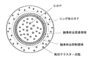
- 前記単結晶が、COPおよび転位クラスターが存在しない無欠陥領域からなることを特徴とする請求項1〜3のいずれかに記載の単結晶の製造方法。
Priority Applications (2)
| Application Number | Priority Date | Filing Date | Title |
|---|---|---|---|
| JP2008181649A JP5223513B2 (ja) | 2008-07-11 | 2008-07-11 | 単結晶の製造方法 |
| US12/458,410 US10066313B2 (en) | 2008-07-11 | 2009-07-10 | Method of producing single crystal |
Applications Claiming Priority (1)
| Application Number | Priority Date | Filing Date | Title |
|---|---|---|---|
| JP2008181649A JP5223513B2 (ja) | 2008-07-11 | 2008-07-11 | 単結晶の製造方法 |
Publications (2)
| Publication Number | Publication Date |
|---|---|
| JP2010018499A true JP2010018499A (ja) | 2010-01-28 |
| JP5223513B2 JP5223513B2 (ja) | 2013-06-26 |
Family
ID=41567495
Family Applications (1)
| Application Number | Title | Priority Date | Filing Date |
|---|---|---|---|
| JP2008181649A Active JP5223513B2 (ja) | 2008-07-11 | 2008-07-11 | 単結晶の製造方法 |
Country Status (2)
| Country | Link |
|---|---|
| US (1) | US10066313B2 (ja) |
| JP (1) | JP5223513B2 (ja) |
Cited By (2)
| Publication number | Priority date | Publication date | Assignee | Title |
|---|---|---|---|---|
| JP2011236092A (ja) * | 2010-05-12 | 2011-11-24 | Shin Etsu Handotai Co Ltd | 単結晶製造装置および単結晶の製造方法 |
| US11634833B2 (en) | 2020-11-25 | 2023-04-25 | Sumco Corporation | Production method of monocrystalline silicon based on an emissivity of a production apparatus |
Families Citing this family (1)
| Publication number | Priority date | Publication date | Assignee | Title |
|---|---|---|---|---|
| CN113529163A (zh) * | 2020-04-17 | 2021-10-22 | 隆基绿能科技股份有限公司 | 一种拉晶方法 |
Citations (8)
| Publication number | Priority date | Publication date | Assignee | Title |
|---|---|---|---|---|
| JPH03122089A (ja) * | 1989-10-05 | 1991-05-24 | Shin Etsu Handotai Co Ltd | Si単結晶中の酸素濃度調整方法およびその装置 |
| JPH09118585A (ja) * | 1995-10-26 | 1997-05-06 | Kokusai Electric Co Ltd | 単結晶引上装置および単結晶の引上方法 |
| JPH11199387A (ja) * | 1998-01-19 | 1999-07-27 | Shin Etsu Handotai Co Ltd | シリコン単結晶の製造方法およびシリコン単結晶ウエーハ |
| WO2002016678A1 (fr) * | 2000-08-18 | 2002-02-28 | Shin-Etsu Handotai Co.,Ltd. | Procede de production d'un monocristal de silicium |
| JP2003089592A (ja) * | 2001-09-11 | 2003-03-28 | Sumitomo Mitsubishi Silicon Corp | 単結晶引上げ方法 |
| JP2005015290A (ja) * | 2003-06-27 | 2005-01-20 | Shin Etsu Handotai Co Ltd | 単結晶の製造方法及び単結晶 |
| JP2007308335A (ja) * | 2006-05-18 | 2007-11-29 | Covalent Materials Corp | 単結晶引上げ方法 |
| JP2008127217A (ja) * | 2006-11-16 | 2008-06-05 | Sumco Techxiv株式会社 | 半導体単結晶製造装置および製造方法 |
Family Cites Families (4)
| Publication number | Priority date | Publication date | Assignee | Title |
|---|---|---|---|---|
| JP4293395B2 (ja) * | 1999-04-28 | 2009-07-08 | Sumco Techxiv株式会社 | Cz法単結晶インゴット製造装置及び方法 |
| TWI265217B (en) * | 2002-11-14 | 2006-11-01 | Komatsu Denshi Kinzoku Kk | Method and device for manufacturing silicon wafer, method for manufacturing silicon single crystal, and device for pulling up silicon single crystal |
| JP2005015313A (ja) * | 2003-06-27 | 2005-01-20 | Shin Etsu Handotai Co Ltd | 単結晶の製造方法及び単結晶 |
| JP4661204B2 (ja) * | 2004-12-16 | 2011-03-30 | 信越半導体株式会社 | 単結晶の製造方法およびアニールウェーハの製造方法ならびにアニールウェーハ |
-
2008
- 2008-07-11 JP JP2008181649A patent/JP5223513B2/ja active Active
-
2009
- 2009-07-10 US US12/458,410 patent/US10066313B2/en active Active
Patent Citations (8)
| Publication number | Priority date | Publication date | Assignee | Title |
|---|---|---|---|---|
| JPH03122089A (ja) * | 1989-10-05 | 1991-05-24 | Shin Etsu Handotai Co Ltd | Si単結晶中の酸素濃度調整方法およびその装置 |
| JPH09118585A (ja) * | 1995-10-26 | 1997-05-06 | Kokusai Electric Co Ltd | 単結晶引上装置および単結晶の引上方法 |
| JPH11199387A (ja) * | 1998-01-19 | 1999-07-27 | Shin Etsu Handotai Co Ltd | シリコン単結晶の製造方法およびシリコン単結晶ウエーハ |
| WO2002016678A1 (fr) * | 2000-08-18 | 2002-02-28 | Shin-Etsu Handotai Co.,Ltd. | Procede de production d'un monocristal de silicium |
| JP2003089592A (ja) * | 2001-09-11 | 2003-03-28 | Sumitomo Mitsubishi Silicon Corp | 単結晶引上げ方法 |
| JP2005015290A (ja) * | 2003-06-27 | 2005-01-20 | Shin Etsu Handotai Co Ltd | 単結晶の製造方法及び単結晶 |
| JP2007308335A (ja) * | 2006-05-18 | 2007-11-29 | Covalent Materials Corp | 単結晶引上げ方法 |
| JP2008127217A (ja) * | 2006-11-16 | 2008-06-05 | Sumco Techxiv株式会社 | 半導体単結晶製造装置および製造方法 |
Cited By (4)
| Publication number | Priority date | Publication date | Assignee | Title |
|---|---|---|---|---|
| JP2011236092A (ja) * | 2010-05-12 | 2011-11-24 | Shin Etsu Handotai Co Ltd | 単結晶製造装置および単結晶の製造方法 |
| US20130032083A1 (en) * | 2010-05-12 | 2013-02-07 | Shin-Etsu Handotai Co., Ltd. | Single-crystal manufacturing apparatus and method for manufacturing single crystal |
| KR101727722B1 (ko) * | 2010-05-12 | 2017-04-18 | 신에쯔 한도타이 가부시키가이샤 | 단결정 제조 장치 및 단결정의 제조 방법 |
| US11634833B2 (en) | 2020-11-25 | 2023-04-25 | Sumco Corporation | Production method of monocrystalline silicon based on an emissivity of a production apparatus |
Also Published As
| Publication number | Publication date |
|---|---|
| JP5223513B2 (ja) | 2013-06-26 |
| US10066313B2 (en) | 2018-09-04 |
| US20100018454A1 (en) | 2010-01-28 |
Similar Documents
| Publication | Publication Date | Title |
|---|---|---|
| TW522456B (en) | Silicon single crystal wafer and method for manufacturing the same | |
| JP2001158690A (ja) | 高品質シリコン単結晶の製造方法 | |
| JP3627498B2 (ja) | シリコン単結晶の製造方法 | |
| JPH10152395A (ja) | シリコン単結晶の製造方法 | |
| JP5163459B2 (ja) | シリコン単結晶の育成方法及びシリコンウェーハの検査方法 | |
| JP3634133B2 (ja) | 結晶欠陥の少ないシリコン単結晶の製造方法及びシリコン単結晶ウエーハ | |
| JP4193610B2 (ja) | 単結晶の製造方法 | |
| JP2005015312A (ja) | 単結晶の製造方法及び単結晶 | |
| JP2007045662A (ja) | 半導体シリコンウェーハおよびその製造方法 | |
| JP2005015313A (ja) | 単結晶の製造方法及び単結晶 | |
| US20240035197A1 (en) | Crystal Puller, Method for Manufacturing Monocrystalline Silicon Ingots and Monocrystalline Silicon Ingots | |
| JP5223513B2 (ja) | 単結晶の製造方法 | |
| JP2008189485A (ja) | シリコン単結晶の製造方法および製造装置 | |
| JP2006273631A (ja) | シリコン単結晶の製造方法およびアニールウェーハおよびアニールウェーハの製造方法 | |
| JP4151474B2 (ja) | 単結晶の製造方法及び単結晶 | |
| EP1591566B1 (en) | Method of producing p-doped silicon single crystal and p-doped n-type silicon single crystal wafe | |
| JP2005015314A (ja) | 単結晶の製造方法及び単結晶 | |
| JP2004149374A (ja) | シリコンウェーハの製造方法 | |
| JP4496723B2 (ja) | 単結晶の製造方法及び単結晶製造装置 | |
| JP4080657B2 (ja) | シリコン単結晶インゴットの製造方法 | |
| JP2005015290A (ja) | 単結晶の製造方法及び単結晶 | |
| JP4501507B2 (ja) | シリコン単結晶育成方法 | |
| JP4577320B2 (ja) | シリコンウェーハの製造方法 | |
| JP2011225409A (ja) | シリコン単結晶の製造方法 | |
| JP2007210820A (ja) | シリコン単結晶の製造方法 |
Legal Events
| Date | Code | Title | Description |
|---|---|---|---|
| A621 | Written request for application examination |
Free format text: JAPANESE INTERMEDIATE CODE: A621 Effective date: 20110705 |
|
| A977 | Report on retrieval |
Free format text: JAPANESE INTERMEDIATE CODE: A971007 Effective date: 20120508 |
|
| A131 | Notification of reasons for refusal |
Free format text: JAPANESE INTERMEDIATE CODE: A131 Effective date: 20120529 |
|
| A521 | Request for written amendment filed |
Free format text: JAPANESE INTERMEDIATE CODE: A523 Effective date: 20120720 |
|
| A131 | Notification of reasons for refusal |
Free format text: JAPANESE INTERMEDIATE CODE: A131 Effective date: 20121009 |
|
| RD02 | Notification of acceptance of power of attorney |
Free format text: JAPANESE INTERMEDIATE CODE: A7422 Effective date: 20121206 |
|
| A521 | Request for written amendment filed |
Free format text: JAPANESE INTERMEDIATE CODE: A523 Effective date: 20121210 |
|
| TRDD | Decision of grant or rejection written | ||
| A01 | Written decision to grant a patent or to grant a registration (utility model) |
Free format text: JAPANESE INTERMEDIATE CODE: A01 Effective date: 20130212 |
|
| A61 | First payment of annual fees (during grant procedure) |
Free format text: JAPANESE INTERMEDIATE CODE: A61 Effective date: 20130225 |
|
| R150 | Certificate of patent or registration of utility model |
Ref document number: 5223513 Country of ref document: JP Free format text: JAPANESE INTERMEDIATE CODE: R150 Free format text: JAPANESE INTERMEDIATE CODE: R150 |
|
| FPAY | Renewal fee payment (event date is renewal date of database) |
Free format text: PAYMENT UNTIL: 20160322 Year of fee payment: 3 |
|
| R250 | Receipt of annual fees |
Free format text: JAPANESE INTERMEDIATE CODE: R250 |
|
| R250 | Receipt of annual fees |
Free format text: JAPANESE INTERMEDIATE CODE: R250 |
|
| R250 | Receipt of annual fees |
Free format text: JAPANESE INTERMEDIATE CODE: R250 |
|
| R250 | Receipt of annual fees |
Free format text: JAPANESE INTERMEDIATE CODE: R250 |
|
| R250 | Receipt of annual fees |
Free format text: JAPANESE INTERMEDIATE CODE: R250 |
|
| R250 | Receipt of annual fees |
Free format text: JAPANESE INTERMEDIATE CODE: R250 |
|
| R250 | Receipt of annual fees |
Free format text: JAPANESE INTERMEDIATE CODE: R250 |
|
| R250 | Receipt of annual fees |
Free format text: JAPANESE INTERMEDIATE CODE: R250 |
|
| R250 | Receipt of annual fees |
Free format text: JAPANESE INTERMEDIATE CODE: R250 |
|
| R250 | Receipt of annual fees |
Free format text: JAPANESE INTERMEDIATE CODE: R250 |