JP2010016058A - レーザ光源装置及びこれを用いたレーザ照射装置 - Google Patents
レーザ光源装置及びこれを用いたレーザ照射装置 Download PDFInfo
- Publication number
- JP2010016058A JP2010016058A JP2008172667A JP2008172667A JP2010016058A JP 2010016058 A JP2010016058 A JP 2010016058A JP 2008172667 A JP2008172667 A JP 2008172667A JP 2008172667 A JP2008172667 A JP 2008172667A JP 2010016058 A JP2010016058 A JP 2010016058A
- Authority
- JP
- Japan
- Prior art keywords
- light source
- laser
- resonator
- source device
- wave
- Prior art date
- Legal status (The legal status is an assumption and is not a legal conclusion. Google has not performed a legal analysis and makes no representation as to the accuracy of the status listed.)
- Granted
Links
Images


Classifications
-
- H—ELECTRICITY
- H01—ELECTRIC ELEMENTS
- H01S—DEVICES USING THE PROCESS OF LIGHT AMPLIFICATION BY STIMULATED EMISSION OF RADIATION [LASER] TO AMPLIFY OR GENERATE LIGHT; DEVICES USING STIMULATED EMISSION OF ELECTROMAGNETIC RADIATION IN WAVE RANGES OTHER THAN OPTICAL
- H01S3/00—Lasers, i.e. devices using stimulated emission of electromagnetic radiation in the infrared, visible or ultraviolet wave range
- H01S3/09—Processes or apparatus for excitation, e.g. pumping
- H01S3/091—Processes or apparatus for excitation, e.g. pumping using optical pumping
- H01S3/094—Processes or apparatus for excitation, e.g. pumping using optical pumping by coherent light
- H01S3/0941—Processes or apparatus for excitation, e.g. pumping using optical pumping by coherent light of a laser diode
- H01S3/09415—Processes or apparatus for excitation, e.g. pumping using optical pumping by coherent light of a laser diode the pumping beam being parallel to the lasing mode of the pumped medium, e.g. end-pumping
-
- H—ELECTRICITY
- H01—ELECTRIC ELEMENTS
- H01S—DEVICES USING THE PROCESS OF LIGHT AMPLIFICATION BY STIMULATED EMISSION OF RADIATION [LASER] TO AMPLIFY OR GENERATE LIGHT; DEVICES USING STIMULATED EMISSION OF ELECTROMAGNETIC RADIATION IN WAVE RANGES OTHER THAN OPTICAL
- H01S2301/00—Functional characteristics
- H01S2301/20—Lasers with a special output beam profile or cross-section, e.g. non-Gaussian
-
- H—ELECTRICITY
- H01—ELECTRIC ELEMENTS
- H01S—DEVICES USING THE PROCESS OF LIGHT AMPLIFICATION BY STIMULATED EMISSION OF RADIATION [LASER] TO AMPLIFY OR GENERATE LIGHT; DEVICES USING STIMULATED EMISSION OF ELECTROMAGNETIC RADIATION IN WAVE RANGES OTHER THAN OPTICAL
- H01S3/00—Lasers, i.e. devices using stimulated emission of electromagnetic radiation in the infrared, visible or ultraviolet wave range
- H01S3/05—Construction or shape of optical resonators; Accommodation of active medium therein; Shape of active medium
- H01S3/08—Construction or shape of optical resonators or components thereof
- H01S3/08059—Constructional details of the reflector, e.g. shape
-
- H—ELECTRICITY
- H01—ELECTRIC ELEMENTS
- H01S—DEVICES USING THE PROCESS OF LIGHT AMPLIFICATION BY STIMULATED EMISSION OF RADIATION [LASER] TO AMPLIFY OR GENERATE LIGHT; DEVICES USING STIMULATED EMISSION OF ELECTROMAGNETIC RADIATION IN WAVE RANGES OTHER THAN OPTICAL
- H01S3/00—Lasers, i.e. devices using stimulated emission of electromagnetic radiation in the infrared, visible or ultraviolet wave range
- H01S3/05—Construction or shape of optical resonators; Accommodation of active medium therein; Shape of active medium
- H01S3/08—Construction or shape of optical resonators or components thereof
- H01S3/08086—Multiple-wavelength emission
-
- H—ELECTRICITY
- H01—ELECTRIC ELEMENTS
- H01S—DEVICES USING THE PROCESS OF LIGHT AMPLIFICATION BY STIMULATED EMISSION OF RADIATION [LASER] TO AMPLIFY OR GENERATE LIGHT; DEVICES USING STIMULATED EMISSION OF ELECTROMAGNETIC RADIATION IN WAVE RANGES OTHER THAN OPTICAL
- H01S3/00—Lasers, i.e. devices using stimulated emission of electromagnetic radiation in the infrared, visible or ultraviolet wave range
- H01S3/05—Construction or shape of optical resonators; Accommodation of active medium therein; Shape of active medium
- H01S3/08—Construction or shape of optical resonators or components thereof
- H01S3/081—Construction or shape of optical resonators or components thereof comprising three or more reflectors
- H01S3/0813—Configuration of resonator
- H01S3/0815—Configuration of resonator having 3 reflectors, e.g. V-shaped resonators
-
- H—ELECTRICITY
- H01—ELECTRIC ELEMENTS
- H01S—DEVICES USING THE PROCESS OF LIGHT AMPLIFICATION BY STIMULATED EMISSION OF RADIATION [LASER] TO AMPLIFY OR GENERATE LIGHT; DEVICES USING STIMULATED EMISSION OF ELECTROMAGNETIC RADIATION IN WAVE RANGES OTHER THAN OPTICAL
- H01S3/00—Lasers, i.e. devices using stimulated emission of electromagnetic radiation in the infrared, visible or ultraviolet wave range
- H01S3/05—Construction or shape of optical resonators; Accommodation of active medium therein; Shape of active medium
- H01S3/08—Construction or shape of optical resonators or components thereof
- H01S3/081—Construction or shape of optical resonators or components thereof comprising three or more reflectors
- H01S3/082—Construction or shape of optical resonators or components thereof comprising three or more reflectors defining a plurality of resonators, e.g. for mode selection or suppression
-
- H—ELECTRICITY
- H01—ELECTRIC ELEMENTS
- H01S—DEVICES USING THE PROCESS OF LIGHT AMPLIFICATION BY STIMULATED EMISSION OF RADIATION [LASER] TO AMPLIFY OR GENERATE LIGHT; DEVICES USING STIMULATED EMISSION OF ELECTROMAGNETIC RADIATION IN WAVE RANGES OTHER THAN OPTICAL
- H01S3/00—Lasers, i.e. devices using stimulated emission of electromagnetic radiation in the infrared, visible or ultraviolet wave range
- H01S3/09—Processes or apparatus for excitation, e.g. pumping
- H01S3/091—Processes or apparatus for excitation, e.g. pumping using optical pumping
- H01S3/094—Processes or apparatus for excitation, e.g. pumping using optical pumping by coherent light
- H01S3/094069—Multi-mode pumping
-
- H—ELECTRICITY
- H01—ELECTRIC ELEMENTS
- H01S—DEVICES USING THE PROCESS OF LIGHT AMPLIFICATION BY STIMULATED EMISSION OF RADIATION [LASER] TO AMPLIFY OR GENERATE LIGHT; DEVICES USING STIMULATED EMISSION OF ELECTROMAGNETIC RADIATION IN WAVE RANGES OTHER THAN OPTICAL
- H01S3/00—Lasers, i.e. devices using stimulated emission of electromagnetic radiation in the infrared, visible or ultraviolet wave range
- H01S3/10—Controlling the intensity, frequency, phase, polarisation or direction of the emitted radiation, e.g. switching, gating, modulating or demodulating
- H01S3/106—Controlling the intensity, frequency, phase, polarisation or direction of the emitted radiation, e.g. switching, gating, modulating or demodulating by controlling devices placed within the cavity
- H01S3/108—Controlling the intensity, frequency, phase, polarisation or direction of the emitted radiation, e.g. switching, gating, modulating or demodulating by controlling devices placed within the cavity using non-linear optical devices, e.g. exhibiting Brillouin or Raman scattering
- H01S3/109—Frequency multiplication, e.g. harmonic generation
-
- H—ELECTRICITY
- H01—ELECTRIC ELEMENTS
- H01S—DEVICES USING THE PROCESS OF LIGHT AMPLIFICATION BY STIMULATED EMISSION OF RADIATION [LASER] TO AMPLIFY OR GENERATE LIGHT; DEVICES USING STIMULATED EMISSION OF ELECTROMAGNETIC RADIATION IN WAVE RANGES OTHER THAN OPTICAL
- H01S3/00—Lasers, i.e. devices using stimulated emission of electromagnetic radiation in the infrared, visible or ultraviolet wave range
- H01S3/10—Controlling the intensity, frequency, phase, polarisation or direction of the emitted radiation, e.g. switching, gating, modulating or demodulating
- H01S3/11—Mode locking; Q-switching; Other giant-pulse techniques, e.g. cavity dumping
- H01S3/1123—Q-switching
- H01S3/113—Q-switching using intracavity saturable absorbers
-
- H10P34/42—
Landscapes
- Physics & Mathematics (AREA)
- Electromagnetism (AREA)
- Engineering & Computer Science (AREA)
- Plasma & Fusion (AREA)
- Optics & Photonics (AREA)
- Optical Modulation, Optical Deflection, Nonlinear Optics, Optical Demodulation, Optical Logic Elements (AREA)
- Lasers (AREA)
- Recrystallisation Techniques (AREA)
Abstract
【解決手段】横マルチモードの光を出射する励起光源1と、共振器を構成し、少なくとも一部から異なる波長の光を外部に出力する共振器ミラー5,8,12と、励起光源1から出射される横マルチモードパターンの光で励起されるレーザ媒質6と、レーザ媒質6での発振により得られる横マルチモードの線状の基本波が照射されて、線状の変換波を出力する波長変換素子10と、を含む。
【選択図】図2
Description
またレーザアニール技術を利用する場合は、安価な大型のガラス、プラスチック等の基板の上に、基板を高温加熱することなく微結晶または多結晶粒を作製できるので、低コスト化と高性能化を図ることができる。
〔1〕第1の実施の形態
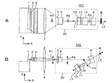
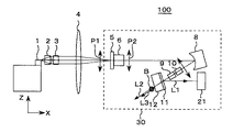
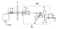
図1及び図2は、本発明の第1の実施の形態に係るレーザ光源装置の概略構成を示す図である。本発明のレーザ光源装置においては、線状の横マルチモードの光を取り扱うものであり、その長手方向をY方向、短軸方向をZ方向、光の進行方向をX方向として示す。図1A及び図2AにおいてはX−Y平面の構成図、図1B及び図2BにおいてはX−Z平面の構成図を示す。
レーザ媒質6としては、希土類添加の固体レーザ材料が用いられ、例えば、Ndイオンをイットリウム・アルミニウム・ガーネット(Y3Al5O12)にドープしたNd:YAG、Nd:YVO4、Nd:GdVO4、Yb:YAG、Yb:YVO4等が挙げられる。
また、それらに分極反転処理を施したPP−C−LiNbO3、PP−C−LiTaO3、PP−S−LiNbO3(PPSLN)、PP−S−LiTaO3(PPSLT)、PP−MgO:C−LiNbO3、PP−MgO:C−LiTaO3等の結晶素子が利用可能である。また、PP−ZnO:C−LiNbO3、PP−ZnO:C−LiTaO3、PP−MgO:S−LiNbO3、PP−MgO:S−LiTaO3、PP−ZnO:S−LiNbO3、PP−ZnO:S−LiTaO3、PP−KTiOPO4等の結晶素子も利用可能である。なおここで、「C」は「congruent(一様融液)組成」、「S」は「Stoichiometric(化学量論的)組成」、「PP」は「Periodical Poling(周期分極反転)」を意味する。
これに対し、上述したように基本波の長手方向を反射部8による折り返し光路の平面内と略垂直な方向とすることによって、基本波の長手方向に関しては、空間的な対称性を保つことができる。したがって、波長変換素子10において変換される変換波においても長手方向に関して空間的な対称性を保つことができるので、非対称化、不均一化を抑制し、結果的に出力光の均一化及び安定化を図ることが可能となる。
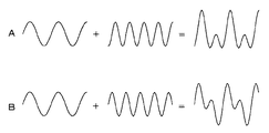
このようにコヒーレンスの高い光を合波する場合、基本波と第2高調波のように波長が倍(半分)の関係にあると、干渉ではないが位相関係によって周期的な強弱のパターンが生じてしまう。波長毎に効果が異なるプロセスに用いる場合は問題ないが、相乗効果などがある場合には、このような強弱のパターンが生じると、プロセスに影響が出て、例えば薄膜トランジスタのSi結晶化工程のアニール等に適用する場合は、結晶粒のばらつきを生じ得る。
一般的に高調波の干渉が十分低減し、安定した出力を得るために必要な空間的ずらし量は、レーザ光の縦横モード数をはじめレーザのもつ特性、また変換波の用途、すなわち適用する光学装置の種類によって異なってくる。一般的には、2つの変換波ビームの光軸を合わせて干渉させた状態に対し、光軸を互いにずらして重ね合わせて発生する干渉縞のビジビリティ(干渉縞コントラスト)が1/e2程度に低減したときのビームずらし量以上であればよい。すなわち、空間干渉距離(空間コヒーレンス長)以上であればよいといえる。
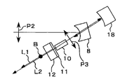
次に、本発明の第2の実施の形態に係るレーザ光源装置について説明する。図8A及びBは第2の実施の形態に係るレーザ光源装置の概略構成図を示す。
本実施の形態においては、第1の実施の形態におけるレーザ光源装置にQスイッチ素子、過飽和吸収体などのパルス生成機構を設けるか、あるいは、レーザダイオード等の励起光源の投入電流値を直接変調する構成とする。このような構成とすることによって、共振器からの基本波と変換波をパルス発振光として取り出すものである。図8A及びBにおいて、図1A及びBと対応する部分には同一符号を付して重複説明を省略する。図8A及びBにおいては、共振器30内のこの場合レーザ媒質6と反射部8との間に、Qスイッチ素子又はCr:YAGなどの透過型過飽和吸収体より成るパルス生成機構20を配置した例である。このパルス生成機構としては、半導体による過飽和吸収体を反射部8や共振器ミラー12等のいずれかの反射面にとりつけても構わない。
なお、本実施の形態における二段階の波長変換を行う例においてはパルス発振とする例を説明したが、必要な変換効率がとれれば連続発振であっても構わないことはいうまでもない。
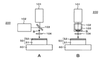
次に、本発明の第3の実施の形態に係るレーザ照射装置の各例を、図12〜図15を参照して説明する。各例共に、上述の第1及び第2の実施の形態において説明した各構成のレーザ光源装置を用いることが可能であり、例えば薄膜トランジスタ(TFT)におけるアモルファスSiなどのレーザアニール工程において適用することができる。本発明によるレーザ光源装置からの変換光、または変換光と基本光からなる線状のレーザビームを、その短軸方向に走査することによって、上述したように、アニールプロセスにおいて徐冷等の好ましい温度変化過程が可能となる。すなわちこのようにレーザプロセス装置として用いることによって、TFTの均質性を保つと共に、性能の向上を図ることが可能となる。
なお、このように相対的な移動手段を設ける場合に、レーザ光照射工程においてのみレーザ光源装置100を載置台60上に配置し、その他の工程においてはレーザ光源装置100が載置台60の上方から待避する構成としてもよい。非照射時の配置構成は、基板等の物質50の載置台60上への出し入れ等の作業やメンテナンス作業等において、作業性を損なわない構成とすることが望ましい。
1.横マルチモードによる低コヒーレンスをもった変換波が得られるため、安定で、容易にトップハット化が可能なレーザ光源装置を実現する。
2.横マルチモード発振により部品点数が少数でも安定性を実現できるので、小型なレーザ光源装置を作ることができる。また、部品点数が少ないため共振器中の損失が小さく高効率なレーザ光源装置を実現することができる。
3.横マルチモードによる低コヒーレンスをもった基本波と変換波の2波長を同時に得られるため、安定で、2波長の干渉がなく、容易にトップハット化可能であるレーザ光源装置を実現する。
4.出力光を、伝搬光路を同一にするための余分な光学系なしに基本波と変換波を同軸で用いることができるようなレーザ光源装置を実現する。
5.ビームの長軸方向にはほぼ同一のビーム径で、短軸には集光位置にて変換波より大きい基本波ビームサイズを持つようなレーザ光源装置を実現する。
6.波長変換素子で発生する高効率な変換波を、基本波、および波長変換素子で逆方向に発生する変換波同士の干渉または位相関係を抑えて取り出し、波長変換素子から両方に発生する変換波同士、あるいは基本波と変換波の2波長が干渉しないまたは位相関係のない状態で用いることができる。
7.長い結晶長を持った波長変換素子により高効率なレーザ光源装置を実現する。また、伝搬方向が全くずれない基本波と変換波が出力されるので、伝搬方向ずれを補正する光学系なしに同軸で基本波と変換波を用いることができる。さらに、形状対称性の高いビームによって均一性の高い基本波及び変換波を出力するレーザ光源装置を実現する。
8.変換波の波長を250nm以上550nm以下となるような波長変換によってレーザ光源装置を構成することができる。
9.出力のばらつきのないレーザ光源装置を実現することができる。
10.高ピークパワーをもつエキシマレーザと比べ安定、メンテナンス不要で複数波長出力のレーザ光源装置を実現することができる。
11.第3高調波などさらに波長の短い波長変換波を出力するレーザ光源装置を実現することができる。さらに、この短波長光と、基本波や変換波との複数波を出力するレーザ光源装置をも実現できる。
1.横マルチモードによる低コヒーレンスで安定な光を用いることから、干渉によるノイズのないプロファイルの均一な安定で高効率なレーザ光源装置が得られる。これにより、例えばSi薄膜トランジスタ、あるいはそのほか太陽電池、LSIなど半導体薄膜素子製造におけるレーザアニールにおいて、照射ビーム強度がばらつかず一定となる。その結果多結晶Siのサイズ均一性を向上させ、粒界を減少させることによって移動度ばらつきを低減することができ、リーク電流減少などの特性の向上を図ることができる。また、横マルチモードにおける波長変換により、このばらつき低減効果を、短波長光を利用したレーザ照射装置にて実現できるので、対象とする物質が短波長光に対して大きな吸収をもつため、移動度を向上しつつばらつきも低減した特性を得ることができる。これは特性向上と歩留向上の両方を実現することを意味する。
特に、基本波と変換波の2波長または3波長のレーザ光を同時に照射することができ、短波長光に対する大きな吸収を利用し、またそれらの光にも干渉や位相関係によるノイズがない、安定で高効率なレーザアニールなどのレーザ照射装置として利用することができる。他にも、Si太陽電池の製造装置の光源、LSI半導体薄膜の製造装置の光源等、その他様々な表面改質プロセス光源、露光光源、加工光源など、種々の材料の表面処理において用いることで、特性の向上を図る効果が得られる。
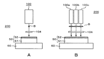
3.レーザアニール装置などにおける小型光源として、アニール対象であるSiトランジスタ基板などの上方に設置することが可能になったり、大面積のSiトランジスタ基板に複数のレーザ光源装置を並列に用いたりすることができる。また、レーザ光源装置側を移動することによってレーザアニールすることが可能であり、これにより大面積のSiトランジスタのアニールを容易にする。更に、複数光源により大面積のSiトランジスタのアニールのタクトタイム減少やスループット向上や特性向上を図ることができる。
Claims (20)
- 横マルチモードの光を出射する励起光源と、
共振器を構成し、少なくとも一部から異なる波長の光を外部に出力する共振器ミラーと、
前記共振器内に配置され、前記励起光源から出射される横マルチモードパターンの光で励起されるレーザ媒質と、
前記共振器内に配置され、前記レーザ媒質での発振により得られる横マルチモードの線状の基本波が照射されて、線状の変換波を出力する波長変換素子と、を含む
レーザ光源装置。 - 前記共振器ミラーのいずれか又は前記共振器内に設けられる折り返し反射部が、前記基本波の一部を透過する構成とされ、
前記基本波と前記変換波が同時に出力される請求項1記載のレーザ光源装置。 - 前記基本波と前記変換波とが、同一方向に出力される請求項1記載のレーザ光源装置。
- 前記波長変換素子から共振光路に沿って両側に変換波が出射され、
前記出射された2本の変換波のうち一方が前記共振器の外部に取り出され、共振器外反射部により前記波長変換素子に戻される構成とされ、
前記共振器外反射部により戻された変換波は、前記波長変換素子で発生する他方の変換波及び基本波とともに、外部に出力される請求項1記載のレーザ光源装置。 - 前記波長変換素子が、擬似位相整合を利用した波長変換素子である請求項1記載のレーザ光源装置。
- 前記レーザ光源装置が連続発振である請求項1記載のレーザ光源装置。
- 前記レーザ光源装置に、パルス生成機構を設け、出力光をパルス発振する請求項1記載のレーザ光源装置。
- 前記パルス生成機構として、前記共振器内にQスイッチ作用を発現するQスイッチ素子又は過飽和吸収体を設ける請求項7記載のレーザ光源装置。
- 前記共振器ミラーの共振光路に構成される共振器内に、前記線状の基本波と前記線状の変換波を照射することによって前記基本波と前記変換波による波長変換波を出力する波長変換素子を更に備える請求項1記載のレーザ光源装置。
- 前記線状の基本波と前記線状の変換波を照射する波長変換素子において、和周波による波長変換波を出力する請求項9記載のレーザ光源装置。
- 横マルチモードの光を出射する励起光源と、共振器を構成し、少なくとも一部から異なる波長の光を前記共振器外に出力する共振器ミラーと、前記共振器内に配置され、前記励起光源から出射される横マルチモードパターンの光で励起されるレーザ媒質と、前記共振器内に配置され、前記レーザ媒質での発振により得られる横マルチモードの線状の基本波が照射されて、線状の変換波を出力する波長変換素子と、を備えるレーザ光源装置と、
前記レーザ光源装置からのレーザ光を照射する物質が載置される載置台と、を備える
レーザ照射装置。 - 前記レーザ光源装置の前記共振器ミラーのいずれかにおいて基本波が一部透過されることによって、前記レーザ光源装置から線状の基本波及び線状の変換波が出力され、
前記線状の基本波及び線状の変換波が前記物質の表面に照射される請求項11記載のレーザ照射装置。 - 前記レーザ光源装置と前記物質が載置される載置台が、前記レーザ光源装置から出力される線状の出力光の短軸方向に相対的に移動して、前記物質に対する照射がなされる請求項11記載のレーザ照射装置。
- 前記レーザ光源装置の前記共振器内に、Qスイッチ作用を発現するQスイッチ素子を備え、前記Qスイッチ素子のQスイッチ作用によって出力光をパルス発振する請求項11記載のレーザ照射装置。
- 前記レーザ光源装置の前記共振器内に、前記線状の基本波と前記線状の変換波を照射することによって前記基本波と前記変換波による波長変換波を出力する波長変換素子を更に備える請求項13記載のレーザ照射装置。
- 前記レーザ光源装置は、前記物質の上方に配置される請求項11記載のレーザ照射装置。
- 前記レーザ光源装置を複数個備え、
前記複数個の前記レーザ光源装置からの出力光が、前記物質の同一の領域に重ね合わせて同時に照射される請求項11記載のレーザ照射装置。 - 複数個の前記レーザ光源装置が並置され、
前記複数個の各レーザ光源装置からの出力光が、前記物質の対応する複数の領域にそれぞれ照射される請求項11記載のレーザ照射装置。 - 横マルチモードの光を出射する励起光源と、共振器を構成する共振器ミラーと、前記共振器内に配置され、前記励起光源から出射される横マルチモードパターンの光で励起されるレーザ媒質と、前記共振器内に配置され、前記レーザ媒質での発振により得られる横マルチモードの線状の基本波が照射されて、線状の変換波を出力する波長変換素子と、を備えるレーザ光源装置と、
前記共振器外に出力されたレーザ光を照射する物質が載置される載置台と、を備える
レーザ照射装置。 - 横マルチモードの光を出射する励起光源と、
共振器を構成する共振器ミラーと、
前記励起光源から出射される横マルチモードパターンの光で励起されるレーザ媒質と、
前記レーザ媒質での発振により得られる横マルチモードの線状の基本波が照射されて、線状の変換波を出力する波長変換素子と、
出力光をパルス発振するパルス生成機構と、を含む
レーザ光源装置。
Priority Applications (3)
| Application Number | Priority Date | Filing Date | Title |
|---|---|---|---|
| JP2008172667A JP4858499B2 (ja) | 2008-07-01 | 2008-07-01 | レーザ光源装置及びこれを用いたレーザ照射装置 |
| US12/490,083 US8331415B2 (en) | 2008-07-01 | 2009-06-23 | Laser light source device and laser irradiation apparatus using the same |
| CN200910151264A CN101621173A (zh) | 2008-07-01 | 2009-07-01 | 激光光源装置及采用该装置的激光照射设备 |
Applications Claiming Priority (1)
| Application Number | Priority Date | Filing Date | Title |
|---|---|---|---|
| JP2008172667A JP4858499B2 (ja) | 2008-07-01 | 2008-07-01 | レーザ光源装置及びこれを用いたレーザ照射装置 |
Publications (2)
| Publication Number | Publication Date |
|---|---|
| JP2010016058A true JP2010016058A (ja) | 2010-01-21 |
| JP4858499B2 JP4858499B2 (ja) | 2012-01-18 |
Family
ID=41464372
Family Applications (1)
| Application Number | Title | Priority Date | Filing Date |
|---|---|---|---|
| JP2008172667A Expired - Fee Related JP4858499B2 (ja) | 2008-07-01 | 2008-07-01 | レーザ光源装置及びこれを用いたレーザ照射装置 |
Country Status (3)
| Country | Link |
|---|---|
| US (1) | US8331415B2 (ja) |
| JP (1) | JP4858499B2 (ja) |
| CN (1) | CN101621173A (ja) |
Cited By (5)
| Publication number | Priority date | Publication date | Assignee | Title |
|---|---|---|---|---|
| CN102145436A (zh) * | 2010-02-09 | 2011-08-10 | 三菱综合材料株式会社 | 激光加工装置 |
| WO2014080520A1 (ja) * | 2012-11-26 | 2014-05-30 | 三菱電機株式会社 | レーザ装置 |
| JP2016065871A (ja) * | 2010-01-22 | 2016-04-28 | ニューポート コーポレーション | 広範に同調可能な光パラメトリック発振器 |
| JP2017213536A (ja) * | 2016-06-01 | 2017-12-07 | 株式会社クリーンプラネット | 還元装置、還元方法およびエネルギー生成・貯蔵システム |
| JP2019140283A (ja) * | 2018-02-13 | 2019-08-22 | 旭化成株式会社 | 金属配線の製造方法及び金属配線製造装置 |
Families Citing this family (166)
| Publication number | Priority date | Publication date | Assignee | Title |
|---|---|---|---|---|
| WO2011148895A1 (ja) | 2010-05-24 | 2011-12-01 | ギガフォトン株式会社 | 固体レーザ装置およびレーザシステム |
| CN101950919A (zh) * | 2010-09-07 | 2011-01-19 | 长春理工大学 | 全固态串联泵浦激光器 |
| CN102074885B (zh) * | 2010-12-29 | 2016-05-04 | 福州高意通讯有限公司 | 一种激光腔内起偏器及激光腔结构 |
| JP5740190B2 (ja) | 2011-03-28 | 2015-06-24 | ギガフォトン株式会社 | レーザシステムおよびレーザ生成方法 |
| EP2523277B1 (de) * | 2011-05-09 | 2017-01-04 | Trumpf Laser Marking Systems AG | Laser-Resonator zur Erzeugung frequenzkonvertierter Laserstrahlung |
| CA2885502A1 (en) * | 2012-05-25 | 2013-11-28 | Cambridge Enterprise Limited | Printing of liquid crystal droplet laser resonators on a wet polymer solution and product made therewith |
| US9113347B2 (en) | 2012-12-05 | 2015-08-18 | At&T Intellectual Property I, Lp | Backhaul link for distributed antenna system |
| US10009065B2 (en) | 2012-12-05 | 2018-06-26 | At&T Intellectual Property I, L.P. | Backhaul link for distributed antenna system |
| US9525524B2 (en) | 2013-05-31 | 2016-12-20 | At&T Intellectual Property I, L.P. | Remote distributed antenna system |
| US9999038B2 (en) | 2013-05-31 | 2018-06-12 | At&T Intellectual Property I, L.P. | Remote distributed antenna system |
| US8897697B1 (en) | 2013-11-06 | 2014-11-25 | At&T Intellectual Property I, Lp | Millimeter-wave surface-wave communications |
| US9209902B2 (en) | 2013-12-10 | 2015-12-08 | At&T Intellectual Property I, L.P. | Quasi-optical coupler |
| US9692101B2 (en) | 2014-08-26 | 2017-06-27 | At&T Intellectual Property I, L.P. | Guided wave couplers for coupling electromagnetic waves between a waveguide surface and a surface of a wire |
| US9768833B2 (en) | 2014-09-15 | 2017-09-19 | At&T Intellectual Property I, L.P. | Method and apparatus for sensing a condition in a transmission medium of electromagnetic waves |
| US10063280B2 (en) | 2014-09-17 | 2018-08-28 | At&T Intellectual Property I, L.P. | Monitoring and mitigating conditions in a communication network |
| US9628854B2 (en) | 2014-09-29 | 2017-04-18 | At&T Intellectual Property I, L.P. | Method and apparatus for distributing content in a communication network |
| US9615269B2 (en) | 2014-10-02 | 2017-04-04 | At&T Intellectual Property I, L.P. | Method and apparatus that provides fault tolerance in a communication network |
| US9685992B2 (en) | 2014-10-03 | 2017-06-20 | At&T Intellectual Property I, L.P. | Circuit panel network and methods thereof |
| US9503189B2 (en) | 2014-10-10 | 2016-11-22 | At&T Intellectual Property I, L.P. | Method and apparatus for arranging communication sessions in a communication system |
| US9973299B2 (en) | 2014-10-14 | 2018-05-15 | At&T Intellectual Property I, L.P. | Method and apparatus for adjusting a mode of communication in a communication network |
| US9762289B2 (en) | 2014-10-14 | 2017-09-12 | At&T Intellectual Property I, L.P. | Method and apparatus for transmitting or receiving signals in a transportation system |
| US9312919B1 (en) | 2014-10-21 | 2016-04-12 | At&T Intellectual Property I, Lp | Transmission device with impairment compensation and methods for use therewith |
| US9780834B2 (en) | 2014-10-21 | 2017-10-03 | At&T Intellectual Property I, L.P. | Method and apparatus for transmitting electromagnetic waves |
| US9577306B2 (en) | 2014-10-21 | 2017-02-21 | At&T Intellectual Property I, L.P. | Guided-wave transmission device and methods for use therewith |
| US9627768B2 (en) | 2014-10-21 | 2017-04-18 | At&T Intellectual Property I, L.P. | Guided-wave transmission device with non-fundamental mode propagation and methods for use therewith |
| US9653770B2 (en) | 2014-10-21 | 2017-05-16 | At&T Intellectual Property I, L.P. | Guided wave coupler, coupling module and methods for use therewith |
| US9520945B2 (en) | 2014-10-21 | 2016-12-13 | At&T Intellectual Property I, L.P. | Apparatus for providing communication services and methods thereof |
| US9769020B2 (en) | 2014-10-21 | 2017-09-19 | At&T Intellectual Property I, L.P. | Method and apparatus for responding to events affecting communications in a communication network |
| US9654173B2 (en) | 2014-11-20 | 2017-05-16 | At&T Intellectual Property I, L.P. | Apparatus for powering a communication device and methods thereof |
| US10243784B2 (en) | 2014-11-20 | 2019-03-26 | At&T Intellectual Property I, L.P. | System for generating topology information and methods thereof |
| US10340573B2 (en) | 2016-10-26 | 2019-07-02 | At&T Intellectual Property I, L.P. | Launcher with cylindrical coupling device and methods for use therewith |
| US9680670B2 (en) | 2014-11-20 | 2017-06-13 | At&T Intellectual Property I, L.P. | Transmission device with channel equalization and control and methods for use therewith |
| US9954287B2 (en) | 2014-11-20 | 2018-04-24 | At&T Intellectual Property I, L.P. | Apparatus for converting wireless signals and electromagnetic waves and methods thereof |
| US9997819B2 (en) | 2015-06-09 | 2018-06-12 | At&T Intellectual Property I, L.P. | Transmission medium and method for facilitating propagation of electromagnetic waves via a core |
| US9800327B2 (en) | 2014-11-20 | 2017-10-24 | At&T Intellectual Property I, L.P. | Apparatus for controlling operations of a communication device and methods thereof |
| US9461706B1 (en) | 2015-07-31 | 2016-10-04 | At&T Intellectual Property I, Lp | Method and apparatus for exchanging communication signals |
| US9544006B2 (en) | 2014-11-20 | 2017-01-10 | At&T Intellectual Property I, L.P. | Transmission device with mode division multiplexing and methods for use therewith |
| US9742462B2 (en) | 2014-12-04 | 2017-08-22 | At&T Intellectual Property I, L.P. | Transmission medium and communication interfaces and methods for use therewith |
| US10009067B2 (en) | 2014-12-04 | 2018-06-26 | At&T Intellectual Property I, L.P. | Method and apparatus for configuring a communication interface |
| US10144036B2 (en) | 2015-01-30 | 2018-12-04 | At&T Intellectual Property I, L.P. | Method and apparatus for mitigating interference affecting a propagation of electromagnetic waves guided by a transmission medium |
| US9876570B2 (en) | 2015-02-20 | 2018-01-23 | At&T Intellectual Property I, Lp | Guided-wave transmission device with non-fundamental mode propagation and methods for use therewith |
| US9749013B2 (en) | 2015-03-17 | 2017-08-29 | At&T Intellectual Property I, L.P. | Method and apparatus for reducing attenuation of electromagnetic waves guided by a transmission medium |
| US9705561B2 (en) | 2015-04-24 | 2017-07-11 | At&T Intellectual Property I, L.P. | Directional coupling device and methods for use therewith |
| US10224981B2 (en) | 2015-04-24 | 2019-03-05 | At&T Intellectual Property I, Lp | Passive electrical coupling device and methods for use therewith |
| US9948354B2 (en) | 2015-04-28 | 2018-04-17 | At&T Intellectual Property I, L.P. | Magnetic coupling device with reflective plate and methods for use therewith |
| US9793954B2 (en) | 2015-04-28 | 2017-10-17 | At&T Intellectual Property I, L.P. | Magnetic coupling device and methods for use therewith |
| US9748626B2 (en) | 2015-05-14 | 2017-08-29 | At&T Intellectual Property I, L.P. | Plurality of cables having different cross-sectional shapes which are bundled together to form a transmission medium |
| US9871282B2 (en) | 2015-05-14 | 2018-01-16 | At&T Intellectual Property I, L.P. | At least one transmission medium having a dielectric surface that is covered at least in part by a second dielectric |
| US9490869B1 (en) | 2015-05-14 | 2016-11-08 | At&T Intellectual Property I, L.P. | Transmission medium having multiple cores and methods for use therewith |
| US10650940B2 (en) | 2015-05-15 | 2020-05-12 | At&T Intellectual Property I, L.P. | Transmission medium having a conductive material and methods for use therewith |
| US9917341B2 (en) | 2015-05-27 | 2018-03-13 | At&T Intellectual Property I, L.P. | Apparatus and method for launching electromagnetic waves and for modifying radial dimensions of the propagating electromagnetic waves |
| US10812174B2 (en) | 2015-06-03 | 2020-10-20 | At&T Intellectual Property I, L.P. | Client node device and methods for use therewith |
| US9866309B2 (en) | 2015-06-03 | 2018-01-09 | At&T Intellectual Property I, Lp | Host node device and methods for use therewith |
| US10103801B2 (en) | 2015-06-03 | 2018-10-16 | At&T Intellectual Property I, L.P. | Host node device and methods for use therewith |
| US9912381B2 (en) | 2015-06-03 | 2018-03-06 | At&T Intellectual Property I, Lp | Network termination and methods for use therewith |
| US9913139B2 (en) | 2015-06-09 | 2018-03-06 | At&T Intellectual Property I, L.P. | Signal fingerprinting for authentication of communicating devices |
| US9608692B2 (en) | 2015-06-11 | 2017-03-28 | At&T Intellectual Property I, L.P. | Repeater and methods for use therewith |
| US10142086B2 (en) | 2015-06-11 | 2018-11-27 | At&T Intellectual Property I, L.P. | Repeater and methods for use therewith |
| US9820146B2 (en) | 2015-06-12 | 2017-11-14 | At&T Intellectual Property I, L.P. | Method and apparatus for authentication and identity management of communicating devices |
| US9667317B2 (en) | 2015-06-15 | 2017-05-30 | At&T Intellectual Property I, L.P. | Method and apparatus for providing security using network traffic adjustments |
| US9509415B1 (en) | 2015-06-25 | 2016-11-29 | At&T Intellectual Property I, L.P. | Methods and apparatus for inducing a fundamental wave mode on a transmission medium |
| US9640850B2 (en) | 2015-06-25 | 2017-05-02 | At&T Intellectual Property I, L.P. | Methods and apparatus for inducing a non-fundamental wave mode on a transmission medium |
| US9865911B2 (en) | 2015-06-25 | 2018-01-09 | At&T Intellectual Property I, L.P. | Waveguide system for slot radiating first electromagnetic waves that are combined into a non-fundamental wave mode second electromagnetic wave on a transmission medium |
| US10205655B2 (en) | 2015-07-14 | 2019-02-12 | At&T Intellectual Property I, L.P. | Apparatus and methods for communicating utilizing an antenna array and multiple communication paths |
| US9722318B2 (en) | 2015-07-14 | 2017-08-01 | At&T Intellectual Property I, L.P. | Method and apparatus for coupling an antenna to a device |
| US10320586B2 (en) | 2015-07-14 | 2019-06-11 | At&T Intellectual Property I, L.P. | Apparatus and methods for generating non-interfering electromagnetic waves on an insulated transmission medium |
| US9836957B2 (en) | 2015-07-14 | 2017-12-05 | At&T Intellectual Property I, L.P. | Method and apparatus for communicating with premises equipment |
| US9882257B2 (en) | 2015-07-14 | 2018-01-30 | At&T Intellectual Property I, L.P. | Method and apparatus for launching a wave mode that mitigates interference |
| US9628116B2 (en) | 2015-07-14 | 2017-04-18 | At&T Intellectual Property I, L.P. | Apparatus and methods for transmitting wireless signals |
| US10033108B2 (en) | 2015-07-14 | 2018-07-24 | At&T Intellectual Property I, L.P. | Apparatus and methods for generating an electromagnetic wave having a wave mode that mitigates interference |
| US10033107B2 (en) | 2015-07-14 | 2018-07-24 | At&T Intellectual Property I, L.P. | Method and apparatus for coupling an antenna to a device |
| US9853342B2 (en) | 2015-07-14 | 2017-12-26 | At&T Intellectual Property I, L.P. | Dielectric transmission medium connector and methods for use therewith |
| US10170840B2 (en) | 2015-07-14 | 2019-01-01 | At&T Intellectual Property I, L.P. | Apparatus and methods for sending or receiving electromagnetic signals |
| US10148016B2 (en) | 2015-07-14 | 2018-12-04 | At&T Intellectual Property I, L.P. | Apparatus and methods for communicating utilizing an antenna array |
| US9847566B2 (en) | 2015-07-14 | 2017-12-19 | At&T Intellectual Property I, L.P. | Method and apparatus for adjusting a field of a signal to mitigate interference |
| US10341142B2 (en) | 2015-07-14 | 2019-07-02 | At&T Intellectual Property I, L.P. | Apparatus and methods for generating non-interfering electromagnetic waves on an uninsulated conductor |
| US10044409B2 (en) | 2015-07-14 | 2018-08-07 | At&T Intellectual Property I, L.P. | Transmission medium and methods for use therewith |
| US10090606B2 (en) | 2015-07-15 | 2018-10-02 | At&T Intellectual Property I, L.P. | Antenna system with dielectric array and methods for use therewith |
| US9793951B2 (en) * | 2015-07-15 | 2017-10-17 | At&T Intellectual Property I, L.P. | Method and apparatus for launching a wave mode that mitigates interference |
| US9608740B2 (en) | 2015-07-15 | 2017-03-28 | At&T Intellectual Property I, L.P. | Method and apparatus for launching a wave mode that mitigates interference |
| US10784670B2 (en) | 2015-07-23 | 2020-09-22 | At&T Intellectual Property I, L.P. | Antenna support for aligning an antenna |
| US9871283B2 (en) | 2015-07-23 | 2018-01-16 | At&T Intellectual Property I, Lp | Transmission medium having a dielectric core comprised of plural members connected by a ball and socket configuration |
| US9912027B2 (en) | 2015-07-23 | 2018-03-06 | At&T Intellectual Property I, L.P. | Method and apparatus for exchanging communication signals |
| US9749053B2 (en) | 2015-07-23 | 2017-08-29 | At&T Intellectual Property I, L.P. | Node device, repeater and methods for use therewith |
| US9948333B2 (en) | 2015-07-23 | 2018-04-17 | At&T Intellectual Property I, L.P. | Method and apparatus for wireless communications to mitigate interference |
| US9735833B2 (en) | 2015-07-31 | 2017-08-15 | At&T Intellectual Property I, L.P. | Method and apparatus for communications management in a neighborhood network |
| US9967173B2 (en) | 2015-07-31 | 2018-05-08 | At&T Intellectual Property I, L.P. | Method and apparatus for authentication and identity management of communicating devices |
| US10020587B2 (en) | 2015-07-31 | 2018-07-10 | At&T Intellectual Property I, L.P. | Radial antenna and methods for use therewith |
| US9904535B2 (en) | 2015-09-14 | 2018-02-27 | At&T Intellectual Property I, L.P. | Method and apparatus for distributing software |
| US10136434B2 (en) | 2015-09-16 | 2018-11-20 | At&T Intellectual Property I, L.P. | Method and apparatus for use with a radio distributed antenna system having an ultra-wideband control channel |
| US10079661B2 (en) | 2015-09-16 | 2018-09-18 | At&T Intellectual Property I, L.P. | Method and apparatus for use with a radio distributed antenna system having a clock reference |
| US10009901B2 (en) | 2015-09-16 | 2018-06-26 | At&T Intellectual Property I, L.P. | Method, apparatus, and computer-readable storage medium for managing utilization of wireless resources between base stations |
| US10051629B2 (en) | 2015-09-16 | 2018-08-14 | At&T Intellectual Property I, L.P. | Method and apparatus for use with a radio distributed antenna system having an in-band reference signal |
| US10009063B2 (en) | 2015-09-16 | 2018-06-26 | At&T Intellectual Property I, L.P. | Method and apparatus for use with a radio distributed antenna system having an out-of-band reference signal |
| US9769128B2 (en) | 2015-09-28 | 2017-09-19 | At&T Intellectual Property I, L.P. | Method and apparatus for encryption of communications over a network |
| US9729197B2 (en) | 2015-10-01 | 2017-08-08 | At&T Intellectual Property I, L.P. | Method and apparatus for communicating network management traffic over a network |
| US9876264B2 (en) | 2015-10-02 | 2018-01-23 | At&T Intellectual Property I, Lp | Communication system, guided wave switch and methods for use therewith |
| US9882277B2 (en) | 2015-10-02 | 2018-01-30 | At&T Intellectual Property I, Lp | Communication device and antenna assembly with actuated gimbal mount |
| US10665942B2 (en) | 2015-10-16 | 2020-05-26 | At&T Intellectual Property I, L.P. | Method and apparatus for adjusting wireless communications |
| US10355367B2 (en) | 2015-10-16 | 2019-07-16 | At&T Intellectual Property I, L.P. | Antenna structure for exchanging wireless signals |
| CN105487291A (zh) * | 2016-01-08 | 2016-04-13 | 京东方科技集团股份有限公司 | 一种背光模组、其制备方法及显示装置 |
| US9912419B1 (en) | 2016-08-24 | 2018-03-06 | At&T Intellectual Property I, L.P. | Method and apparatus for managing a fault in a distributed antenna system |
| US9860075B1 (en) | 2016-08-26 | 2018-01-02 | At&T Intellectual Property I, L.P. | Method and communication node for broadband distribution |
| US10291311B2 (en) | 2016-09-09 | 2019-05-14 | At&T Intellectual Property I, L.P. | Method and apparatus for mitigating a fault in a distributed antenna system |
| US11032819B2 (en) | 2016-09-15 | 2021-06-08 | At&T Intellectual Property I, L.P. | Method and apparatus for use with a radio distributed antenna system having a control channel reference signal |
| US10135146B2 (en) | 2016-10-18 | 2018-11-20 | At&T Intellectual Property I, L.P. | Apparatus and methods for launching guided waves via circuits |
| US10135147B2 (en) | 2016-10-18 | 2018-11-20 | At&T Intellectual Property I, L.P. | Apparatus and methods for launching guided waves via an antenna |
| US10340600B2 (en) | 2016-10-18 | 2019-07-02 | At&T Intellectual Property I, L.P. | Apparatus and methods for launching guided waves via plural waveguide systems |
| US9876605B1 (en) | 2016-10-21 | 2018-01-23 | At&T Intellectual Property I, L.P. | Launcher and coupling system to support desired guided wave mode |
| US10374316B2 (en) | 2016-10-21 | 2019-08-06 | At&T Intellectual Property I, L.P. | System and dielectric antenna with non-uniform dielectric |
| US9991580B2 (en) | 2016-10-21 | 2018-06-05 | At&T Intellectual Property I, L.P. | Launcher and coupling system for guided wave mode cancellation |
| US10811767B2 (en) | 2016-10-21 | 2020-10-20 | At&T Intellectual Property I, L.P. | System and dielectric antenna with convex dielectric radome |
| US10312567B2 (en) | 2016-10-26 | 2019-06-04 | At&T Intellectual Property I, L.P. | Launcher with planar strip antenna and methods for use therewith |
| US10291334B2 (en) | 2016-11-03 | 2019-05-14 | At&T Intellectual Property I, L.P. | System for detecting a fault in a communication system |
| US10225025B2 (en) | 2016-11-03 | 2019-03-05 | At&T Intellectual Property I, L.P. | Method and apparatus for detecting a fault in a communication system |
| US10498044B2 (en) | 2016-11-03 | 2019-12-03 | At&T Intellectual Property I, L.P. | Apparatus for configuring a surface of an antenna |
| US10224634B2 (en) | 2016-11-03 | 2019-03-05 | At&T Intellectual Property I, L.P. | Methods and apparatus for adjusting an operational characteristic of an antenna |
| US10178445B2 (en) | 2016-11-23 | 2019-01-08 | At&T Intellectual Property I, L.P. | Methods, devices, and systems for load balancing between a plurality of waveguides |
| US10340603B2 (en) | 2016-11-23 | 2019-07-02 | At&T Intellectual Property I, L.P. | Antenna system having shielded structural configurations for assembly |
| US10090594B2 (en) | 2016-11-23 | 2018-10-02 | At&T Intellectual Property I, L.P. | Antenna system having structural configurations for assembly |
| US10340601B2 (en) | 2016-11-23 | 2019-07-02 | At&T Intellectual Property I, L.P. | Multi-antenna system and methods for use therewith |
| US10535928B2 (en) | 2016-11-23 | 2020-01-14 | At&T Intellectual Property I, L.P. | Antenna system and methods for use therewith |
| US10361489B2 (en) | 2016-12-01 | 2019-07-23 | At&T Intellectual Property I, L.P. | Dielectric dish antenna system and methods for use therewith |
| US10305190B2 (en) | 2016-12-01 | 2019-05-28 | At&T Intellectual Property I, L.P. | Reflecting dielectric antenna system and methods for use therewith |
| US10637149B2 (en) | 2016-12-06 | 2020-04-28 | At&T Intellectual Property I, L.P. | Injection molded dielectric antenna and methods for use therewith |
| US10326494B2 (en) | 2016-12-06 | 2019-06-18 | At&T Intellectual Property I, L.P. | Apparatus for measurement de-embedding and methods for use therewith |
| US10727599B2 (en) | 2016-12-06 | 2020-07-28 | At&T Intellectual Property I, L.P. | Launcher with slot antenna and methods for use therewith |
| US10694379B2 (en) | 2016-12-06 | 2020-06-23 | At&T Intellectual Property I, L.P. | Waveguide system with device-based authentication and methods for use therewith |
| US9927517B1 (en) | 2016-12-06 | 2018-03-27 | At&T Intellectual Property I, L.P. | Apparatus and methods for sensing rainfall |
| US10382976B2 (en) | 2016-12-06 | 2019-08-13 | At&T Intellectual Property I, L.P. | Method and apparatus for managing wireless communications based on communication paths and network device positions |
| US10020844B2 (en) | 2016-12-06 | 2018-07-10 | T&T Intellectual Property I, L.P. | Method and apparatus for broadcast communication via guided waves |
| US10135145B2 (en) | 2016-12-06 | 2018-11-20 | At&T Intellectual Property I, L.P. | Apparatus and methods for generating an electromagnetic wave along a transmission medium |
| US10755542B2 (en) | 2016-12-06 | 2020-08-25 | At&T Intellectual Property I, L.P. | Method and apparatus for surveillance via guided wave communication |
| US10819035B2 (en) | 2016-12-06 | 2020-10-27 | At&T Intellectual Property I, L.P. | Launcher with helical antenna and methods for use therewith |
| US10439675B2 (en) | 2016-12-06 | 2019-10-08 | At&T Intellectual Property I, L.P. | Method and apparatus for repeating guided wave communication signals |
| US10547348B2 (en) | 2016-12-07 | 2020-01-28 | At&T Intellectual Property I, L.P. | Method and apparatus for switching transmission mediums in a communication system |
| US9893795B1 (en) | 2016-12-07 | 2018-02-13 | At&T Intellectual Property I, Lp | Method and repeater for broadband distribution |
| US10027397B2 (en) | 2016-12-07 | 2018-07-17 | At&T Intellectual Property I, L.P. | Distributed antenna system and methods for use therewith |
| US10389029B2 (en) | 2016-12-07 | 2019-08-20 | At&T Intellectual Property I, L.P. | Multi-feed dielectric antenna system with core selection and methods for use therewith |
| US10243270B2 (en) | 2016-12-07 | 2019-03-26 | At&T Intellectual Property I, L.P. | Beam adaptive multi-feed dielectric antenna system and methods for use therewith |
| US10446936B2 (en) | 2016-12-07 | 2019-10-15 | At&T Intellectual Property I, L.P. | Multi-feed dielectric antenna system and methods for use therewith |
| US10359749B2 (en) | 2016-12-07 | 2019-07-23 | At&T Intellectual Property I, L.P. | Method and apparatus for utilities management via guided wave communication |
| US10139820B2 (en) | 2016-12-07 | 2018-11-27 | At&T Intellectual Property I, L.P. | Method and apparatus for deploying equipment of a communication system |
| US10168695B2 (en) | 2016-12-07 | 2019-01-01 | At&T Intellectual Property I, L.P. | Method and apparatus for controlling an unmanned aircraft |
| US10777873B2 (en) | 2016-12-08 | 2020-09-15 | At&T Intellectual Property I, L.P. | Method and apparatus for mounting network devices |
| US10916969B2 (en) | 2016-12-08 | 2021-02-09 | At&T Intellectual Property I, L.P. | Method and apparatus for providing power using an inductive coupling |
| US9911020B1 (en) | 2016-12-08 | 2018-03-06 | At&T Intellectual Property I, L.P. | Method and apparatus for tracking via a radio frequency identification device |
| US10938108B2 (en) | 2016-12-08 | 2021-03-02 | At&T Intellectual Property I, L.P. | Frequency selective multi-feed dielectric antenna system and methods for use therewith |
| US10069535B2 (en) | 2016-12-08 | 2018-09-04 | At&T Intellectual Property I, L.P. | Apparatus and methods for launching electromagnetic waves having a certain electric field structure |
| US10530505B2 (en) | 2016-12-08 | 2020-01-07 | At&T Intellectual Property I, L.P. | Apparatus and methods for launching electromagnetic waves along a transmission medium |
| US10103422B2 (en) | 2016-12-08 | 2018-10-16 | At&T Intellectual Property I, L.P. | Method and apparatus for mounting network devices |
| US10326689B2 (en) | 2016-12-08 | 2019-06-18 | At&T Intellectual Property I, L.P. | Method and system for providing alternative communication paths |
| US10389037B2 (en) | 2016-12-08 | 2019-08-20 | At&T Intellectual Property I, L.P. | Apparatus and methods for selecting sections of an antenna array and use therewith |
| US10411356B2 (en) | 2016-12-08 | 2019-09-10 | At&T Intellectual Property I, L.P. | Apparatus and methods for selectively targeting communication devices with an antenna array |
| US9998870B1 (en) | 2016-12-08 | 2018-06-12 | At&T Intellectual Property I, L.P. | Method and apparatus for proximity sensing |
| US10601494B2 (en) | 2016-12-08 | 2020-03-24 | At&T Intellectual Property I, L.P. | Dual-band communication device and method for use therewith |
| US10264586B2 (en) | 2016-12-09 | 2019-04-16 | At&T Mobility Ii Llc | Cloud-based packet controller and methods for use therewith |
| US9838896B1 (en) | 2016-12-09 | 2017-12-05 | At&T Intellectual Property I, L.P. | Method and apparatus for assessing network coverage |
| US10340983B2 (en) | 2016-12-09 | 2019-07-02 | At&T Intellectual Property I, L.P. | Method and apparatus for surveying remote sites via guided wave communications |
| US9973940B1 (en) | 2017-02-27 | 2018-05-15 | At&T Intellectual Property I, L.P. | Apparatus and methods for dynamic impedance matching of a guided wave launcher |
| US10298293B2 (en) | 2017-03-13 | 2019-05-21 | At&T Intellectual Property I, L.P. | Apparatus of communication utilizing wireless network devices |
| CN108581189B (zh) * | 2018-06-01 | 2020-04-17 | 业成科技(成都)有限公司 | 激光切割方法 |
| WO2020166420A1 (ja) | 2019-02-13 | 2020-08-20 | ソニー株式会社 | レーザ加工機、加工方法及びレーザ光源 |
| DE102019112141A1 (de) * | 2019-05-09 | 2020-11-12 | Innovavent Gmbh | Verfahren und optisches System zur Bearbeitung eines Halbleitermaterials |
| CN113363798B (zh) * | 2021-05-20 | 2022-09-23 | 厦门大学 | 一种可调控高光学效率宽带多纵模拉曼微片激光器 |
| CN114647010B (zh) * | 2021-12-03 | 2023-04-07 | 吉林大学 | 一种适用于井下长期稳定工作的总场泵源装置及工作方法 |
Citations (6)
| Publication number | Priority date | Publication date | Assignee | Title |
|---|---|---|---|---|
| JPS50148096A (ja) * | 1974-05-20 | 1975-11-27 | ||
| JPH11326971A (ja) * | 1998-05-19 | 1999-11-26 | Mitsubishi Heavy Ind Ltd | 和周波数発生装置 |
| JP2003347237A (ja) * | 2002-05-30 | 2003-12-05 | Mitsubishi Electric Corp | 半導体装置の製造方法およびその製造装置 |
| JP2006066818A (ja) * | 2004-08-30 | 2006-03-09 | Sony Corp | 1次元照明装置及び画像生成装置 |
| JP2006140919A (ja) * | 2004-11-15 | 2006-06-01 | Canon Inc | 撮像装置及び撮像装置の制御方法 |
| JP2008112846A (ja) * | 2006-10-30 | 2008-05-15 | Sony Corp | レーザ光源装置及びこれを用いた画像生成装置 |
Family Cites Families (4)
| Publication number | Priority date | Publication date | Assignee | Title |
|---|---|---|---|---|
| US5157754A (en) * | 1990-04-25 | 1992-10-20 | E. I. Du Pont De Nemours | Wavelength conversion by quasi phase matching and the manufacture and use of optical articles therefor |
| US5473409A (en) * | 1993-09-21 | 1995-12-05 | Sony Corporation | Semiconductor light exposure device |
| US7164810B2 (en) * | 2001-11-21 | 2007-01-16 | Metrologic Instruments, Inc. | Planar light illumination and linear imaging (PLILIM) device with image-based velocity detection and aspect ratio compensation |
| US20060018355A1 (en) * | 2004-07-23 | 2006-01-26 | Comlasc.Nt-Ab | Laser diode arrays with reduced heat induced strain and stress |
-
2008
- 2008-07-01 JP JP2008172667A patent/JP4858499B2/ja not_active Expired - Fee Related
-
2009
- 2009-06-23 US US12/490,083 patent/US8331415B2/en not_active Expired - Fee Related
- 2009-07-01 CN CN200910151264A patent/CN101621173A/zh active Pending
Patent Citations (6)
| Publication number | Priority date | Publication date | Assignee | Title |
|---|---|---|---|---|
| JPS50148096A (ja) * | 1974-05-20 | 1975-11-27 | ||
| JPH11326971A (ja) * | 1998-05-19 | 1999-11-26 | Mitsubishi Heavy Ind Ltd | 和周波数発生装置 |
| JP2003347237A (ja) * | 2002-05-30 | 2003-12-05 | Mitsubishi Electric Corp | 半導体装置の製造方法およびその製造装置 |
| JP2006066818A (ja) * | 2004-08-30 | 2006-03-09 | Sony Corp | 1次元照明装置及び画像生成装置 |
| JP2006140919A (ja) * | 2004-11-15 | 2006-06-01 | Canon Inc | 撮像装置及び撮像装置の制御方法 |
| JP2008112846A (ja) * | 2006-10-30 | 2008-05-15 | Sony Corp | レーザ光源装置及びこれを用いた画像生成装置 |
Cited By (8)
| Publication number | Priority date | Publication date | Assignee | Title |
|---|---|---|---|---|
| JP2016065871A (ja) * | 2010-01-22 | 2016-04-28 | ニューポート コーポレーション | 広範に同調可能な光パラメトリック発振器 |
| CN102145436A (zh) * | 2010-02-09 | 2011-08-10 | 三菱综合材料株式会社 | 激光加工装置 |
| JP2011161483A (ja) * | 2010-02-09 | 2011-08-25 | Mitsubishi Materials Corp | レーザ加工装置 |
| WO2014080520A1 (ja) * | 2012-11-26 | 2014-05-30 | 三菱電機株式会社 | レーザ装置 |
| JP5826409B2 (ja) * | 2012-11-26 | 2015-12-02 | 三菱電機株式会社 | レーザ装置 |
| JP2017213536A (ja) * | 2016-06-01 | 2017-12-07 | 株式会社クリーンプラネット | 還元装置、還元方法およびエネルギー生成・貯蔵システム |
| JP2019140283A (ja) * | 2018-02-13 | 2019-08-22 | 旭化成株式会社 | 金属配線の製造方法及び金属配線製造装置 |
| JP7254444B2 (ja) | 2018-02-13 | 2023-04-10 | 旭化成株式会社 | 金属配線の製造方法及び金属配線製造装置 |
Also Published As
| Publication number | Publication date |
|---|---|
| CN101621173A (zh) | 2010-01-06 |
| US20100002731A1 (en) | 2010-01-07 |
| US8331415B2 (en) | 2012-12-11 |
| JP4858499B2 (ja) | 2012-01-18 |
Similar Documents
| Publication | Publication Date | Title |
|---|---|---|
| JP4858499B2 (ja) | レーザ光源装置及びこれを用いたレーザ照射装置 | |
| CN1145244C (zh) | 波长转换器 | |
| US5803965A (en) | Method and system for manufacturing semiconductor device | |
| KR102344775B1 (ko) | 제3 고조파 생성을 위한 고효율 레이저 시스템 | |
| JPWO2008114512A1 (ja) | レーザ波長変換装置及びこれを備えた画像表示装置 | |
| KR102786318B1 (ko) | 레이저 어닐링을 위한 다이오드 펌핑 고체 레이저 장치 | |
| CN104577696B (zh) | Q开关激光装置 | |
| CN101473498A (zh) | 减少用于激光高功率频率变换的非线性晶体的表面热效应 | |
| CN103500911B (zh) | 一种多点的表面垂直发射的太赫兹参量振荡器及其应用 | |
| US20100074296A1 (en) | Solid state laser and wavelength conversion laser | |
| JP5721812B2 (ja) | 波長変換結晶および波長変換レーザ装置 | |
| JP4826558B2 (ja) | レーザー装置 | |
| ES2283149T3 (es) | Dispositivos de laser semiconductores de bo,beo optico con cavidad externa, de alta potencia. | |
| JP2009182353A (ja) | レーザ光源装置及びこれを用いた画像生成装置 | |
| US6807210B2 (en) | Systems and a method for generating blue laser beam | |
| CN100421316C (zh) | 四次谐波固体激光产生方法 | |
| CN101383477A (zh) | 激光二次谐波发生装置 | |
| JP2004289140A (ja) | レーザ照射装置及びレーザ照射方法並びに半導体装置の作製方法。 | |
| WO2015052744A1 (ja) | レーザ装置 | |
| JP2000338530A (ja) | レーザ光の波長変換装置とその変換方法 | |
| JP2008153526A (ja) | レーザ光源装置及びこれを用いた画像生成装置 | |
| JP2007266537A (ja) | 内部共振器型和周波混合レーザ | |
| JPH09331097A (ja) | 固体レーザ装置 | |
| JP2008066356A (ja) | レーザアニール方法および装置 | |
| Ai-Yun et al. | High power red laser at 671nm by intracavity frequency doubling of a Nd: YVO4 laser |
Legal Events
| Date | Code | Title | Description |
|---|---|---|---|
| A131 | Notification of reasons for refusal |
Free format text: JAPANESE INTERMEDIATE CODE: A131 Effective date: 20100209 |
|
| A521 | Request for written amendment filed |
Free format text: JAPANESE INTERMEDIATE CODE: A523 Effective date: 20100405 |
|
| A131 | Notification of reasons for refusal |
Free format text: JAPANESE INTERMEDIATE CODE: A131 Effective date: 20110111 |
|
| TRDD | Decision of grant or rejection written | ||
| A01 | Written decision to grant a patent or to grant a registration (utility model) |
Free format text: JAPANESE INTERMEDIATE CODE: A01 Effective date: 20111004 |
|
| A01 | Written decision to grant a patent or to grant a registration (utility model) |
Free format text: JAPANESE INTERMEDIATE CODE: A01 |
|
| A61 | First payment of annual fees (during grant procedure) |
Free format text: JAPANESE INTERMEDIATE CODE: A61 Effective date: 20111017 |
|
| R151 | Written notification of patent or utility model registration |
Ref document number: 4858499 Country of ref document: JP Free format text: JAPANESE INTERMEDIATE CODE: R151 |
|
| FPAY | Renewal fee payment (event date is renewal date of database) |
Free format text: PAYMENT UNTIL: 20141111 Year of fee payment: 3 |
|
| R250 | Receipt of annual fees |
Free format text: JAPANESE INTERMEDIATE CODE: R250 |
|
| R250 | Receipt of annual fees |
Free format text: JAPANESE INTERMEDIATE CODE: R250 |
|
| R250 | Receipt of annual fees |
Free format text: JAPANESE INTERMEDIATE CODE: R250 |
|
| R250 | Receipt of annual fees |
Free format text: JAPANESE INTERMEDIATE CODE: R250 |
|
| R250 | Receipt of annual fees |
Free format text: JAPANESE INTERMEDIATE CODE: R250 |
|
| R250 | Receipt of annual fees |
Free format text: JAPANESE INTERMEDIATE CODE: R250 |
|
| R250 | Receipt of annual fees |
Free format text: JAPANESE INTERMEDIATE CODE: R250 |
|
| LAPS | Cancellation because of no payment of annual fees |