JP2010009964A - 有機elパネル製造方法および製造装置 - Google Patents
有機elパネル製造方法および製造装置 Download PDFInfo
- Publication number
- JP2010009964A JP2010009964A JP2008168689A JP2008168689A JP2010009964A JP 2010009964 A JP2010009964 A JP 2010009964A JP 2008168689 A JP2008168689 A JP 2008168689A JP 2008168689 A JP2008168689 A JP 2008168689A JP 2010009964 A JP2010009964 A JP 2010009964A
- Authority
- JP
- Japan
- Prior art keywords
- organic
- filter
- color filter
- panel
- leak
- Prior art date
- Legal status (The legal status is an assumption and is not a legal conclusion. Google has not performed a legal analysis and makes no representation as to the accuracy of the status listed.)
- Granted
Links
- 238000004519 manufacturing process Methods 0.000 title claims description 49
- 238000007689 inspection Methods 0.000 claims description 44
- 238000000034 method Methods 0.000 claims description 30
- 230000008569 process Effects 0.000 claims description 21
- 230000005540 biological transmission Effects 0.000 claims description 16
- 238000003384 imaging method Methods 0.000 claims description 12
- 230000002950 deficient Effects 0.000 claims description 4
- 230000001747 exhibiting effect Effects 0.000 claims 1
- 238000001514 detection method Methods 0.000 abstract description 28
- 238000002834 transmittance Methods 0.000 description 17
- 238000010586 diagram Methods 0.000 description 16
- 230000007547 defect Effects 0.000 description 15
- 239000000758 substrate Substances 0.000 description 14
- 230000004075 alteration Effects 0.000 description 13
- 239000011521 glass Substances 0.000 description 13
- 230000003595 spectral effect Effects 0.000 description 13
- 230000008859 change Effects 0.000 description 8
- 230000000007 visual effect Effects 0.000 description 8
- 230000007423 decrease Effects 0.000 description 6
- 238000001228 spectrum Methods 0.000 description 5
- WUKWITHWXAAZEY-UHFFFAOYSA-L calcium difluoride Chemical compound [F-].[F-].[Ca+2] WUKWITHWXAAZEY-UHFFFAOYSA-L 0.000 description 3
- 239000010436 fluorite Substances 0.000 description 3
- 239000004973 liquid crystal related substance Substances 0.000 description 3
- 239000000463 material Substances 0.000 description 3
- 239000002184 metal Substances 0.000 description 2
- 230000003287 optical effect Effects 0.000 description 2
- 150000002894 organic compounds Chemical class 0.000 description 2
- 230000008439 repair process Effects 0.000 description 2
- 230000035945 sensitivity Effects 0.000 description 2
- 239000000126 substance Substances 0.000 description 2
- 230000000699 topical effect Effects 0.000 description 2
- 229910000831 Steel Inorganic materials 0.000 description 1
- 239000000470 constituent Substances 0.000 description 1
- 238000007796 conventional method Methods 0.000 description 1
- 230000006866 deterioration Effects 0.000 description 1
- 239000006185 dispersion Substances 0.000 description 1
- 230000007935 neutral effect Effects 0.000 description 1
- 230000002093 peripheral effect Effects 0.000 description 1
- 239000000049 pigment Substances 0.000 description 1
- 230000009467 reduction Effects 0.000 description 1
- 230000004044 response Effects 0.000 description 1
- 239000010959 steel Substances 0.000 description 1
Images


Classifications
-
- H—ELECTRICITY
- H10—SEMICONDUCTOR DEVICES; ELECTRIC SOLID-STATE DEVICES NOT OTHERWISE PROVIDED FOR
- H10K—ORGANIC ELECTRIC SOLID-STATE DEVICES
- H10K59/00—Integrated devices, or assemblies of multiple devices, comprising at least one organic light-emitting element covered by group H10K50/00
- H10K59/30—Devices specially adapted for multicolour light emission
- H10K59/38—Devices specially adapted for multicolour light emission comprising colour filters or colour changing media [CCM]
-
- H—ELECTRICITY
- H10—SEMICONDUCTOR DEVICES; ELECTRIC SOLID-STATE DEVICES NOT OTHERWISE PROVIDED FOR
- H10K—ORGANIC ELECTRIC SOLID-STATE DEVICES
- H10K71/00—Manufacture or treatment specially adapted for the organic devices covered by this subclass
-
- H—ELECTRICITY
- H10—SEMICONDUCTOR DEVICES; ELECTRIC SOLID-STATE DEVICES NOT OTHERWISE PROVIDED FOR
- H10K—ORGANIC ELECTRIC SOLID-STATE DEVICES
- H10K71/00—Manufacture or treatment specially adapted for the organic devices covered by this subclass
- H10K71/60—Forming conductive regions or layers, e.g. electrodes
-
- H—ELECTRICITY
- H10—SEMICONDUCTOR DEVICES; ELECTRIC SOLID-STATE DEVICES NOT OTHERWISE PROVIDED FOR
- H10K—ORGANIC ELECTRIC SOLID-STATE DEVICES
- H10K71/00—Manufacture or treatment specially adapted for the organic devices covered by this subclass
- H10K71/861—Repairing
Landscapes
- Engineering & Computer Science (AREA)
- Manufacturing & Machinery (AREA)
- Electroluminescent Light Sources (AREA)
Abstract
【解決手段】各色のフィルタ種別毎に個別電圧値を印加するフィルタ部個別電圧値設定部を備え、赤フィルタの例では、赤フィルタ部個別電圧値設定部54を備え、リーク光(赤フィルタ画素)の性質として、印加電圧によってリーク光強度が変わることを利用し、赤カラーフィルタを通過したリーク発光量に応じた電圧値設定を行うことにより、基準リーク発光量が全フィルタ種別で等価となるように制御することにより、高速高精度にリーク発光を検出することを可能にする。
【選択図】図1
Description
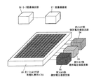
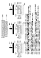
図1は本発明の実施の形態1における有機EL製造装置の構成図である。なお、本実施の形態では、基本的に図15に示すような赤,緑,青のカラーフィルタが設けられた有機ELパネルを例示している。
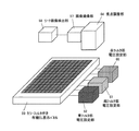
図4は本発明の実施の形態2における有機ELパネル製造装置の構成図であって、図1と同じ構成要素については同じ符号を用い、説明を省略する。
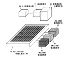
図7は本発明の実施の形態3における有機EL製造装置の構成図であって、図5において、図1,図3と同じ構成要素については同じ符号を用い、その説明を省略する。なお、図5において、64は焦点調整部である。
図9は本発明の実施の形態4における有機ELパネル製造装置の構成図であって、図1,図4,図7と同じ構成要素については同じ符号を用い、その説明を省略する。なお、図9において、65は画像撮像部位置設定部である。
図12は本発明の実施の形態5における有機EL製造装置における要部の説明図であって、29は赤フィルタ、30は緑フィルタ、31は青フィルタ、32は赤用光源、33は緑用光源、34は青用光源、35は赤用光源からの出射光、36は緑用光源からの出射光、37は青用光源からの出射光、38は赤フィルタを通過した赤用光源からの出射光、39は緑フィルタを通過した緑用光源からの出射光、40は青フィルタを通過した青用光源からの出射光である。
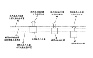
図13は本発明の実施の形態6における有機ELパネル製造装置における要部の説明図であって、41は赤用非赤外光源、42は緑用非赤外光源、43は青用非赤外光源、44は赤用非赤外光源出射光焦点基準面、45は緑用非赤外光源出射光焦点基準面、46は青用非赤外光源出射光焦点基準面、47は赤用非赤外光源からの出射光、48は緑用非赤外光源からの出射光、49は青用非赤外光源からの出射光である。
20 陰極
21 有機EL層
22 基板
23 凹凸部もしくは異物
24 電源
25 リーク光
26 表示パネル
27 表示部
28 ダミー有機EL発光部
29 赤フィルタ
30 緑フィルタ
31 青フィルタ
32 赤用光源
33 緑用光源
34 青用光源
35 赤用光源
36 緑用光源からの出射光
37 青用光源からの出射光
38 赤フィルタを通過した赤用光源からの出射光
39 緑フィルタを通過した緑用光源からの出射光
40 青フィルタを通過した青用光源からの出射光
41 赤用非赤外光源
42 緑用非赤外光源
43 青用非赤外光源
44 赤用非赤外光源出射光焦点基準面
45 緑用非赤外光源出射光焦点基準面
46 青用非赤外光源出射光焦点基準面
47 赤用非赤外光源からの出射光
48 緑用非赤外光源からの出射光
49 青用非赤外光源からの出射光
54 赤フィルタ部個別電圧値設定部
55 緑フィルタ部個別電圧値設定部
56 青フィルタ部個別電圧値設定部
57 画像撮像部
58 リーク画像検出部
59 カラーフィルタ付き有機EL表示パネル
60 赤フィルタ部電圧設定部
61 緑フィルタ部電圧値設定部
62 青フィルタ部電圧設定部
63 コントローラ部
64 焦点調整部
65 画像撮像部位置設定部
100 陽極
101 陽極(赤フィルタ)
102 陽極(緑フィルタ)
103 陽極(青フィルタ)
110 正孔
200 陰極
201 陰極(赤フィルタ)
202 陰極(緑フィルタ)
203 陰極(青フィルタ)
210 電子
300 有機EL層
301 有機EL層(赤フィルタ)
302 有機EL層(緑フィルタ)
303 有機EL層(青フィルタ)
309 異物
400 ガラス基板
401 ガラス基板(赤フィルタ)
402 ガラス基板(緑フィルタ)
403 ガラス基板(青フィルタ)
500 カラーフィルタ
501 赤カラーフィルタ
502 緑カラーフィルタ
503 青カラーフィルタ
601 電流リーク発生箇所(赤フィルタ)
602 電流リーク発生箇所(緑フィルタ)
603 電流リーク発生箇所(青フィルタ)
701 リーク発光(赤フィルタ)
702 リーク発光(緑フィルタ)
703 リーク発光(青フィルタ)
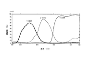
801 赤カラーフィルタを通過したリーク発光
802 緑カラーフィルタを通過したリーク発光
803 青カラーフィルタを通過したリーク発光
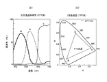
804 赤カラーフィルタを通過したリーク発光量(可視〜赤外波長域)
805 緑カラーフィルタを通過したリーク発光量(可視〜赤外波長域)
806 青カラーフィルタを通過したリーク発光量(可視〜赤外波長域)
807 赤カラーフィルタを通過したリーク発光量(赤外波長域)
808 緑カラーフィルタを通過したリーク発光量(赤外波長域)
809 青カラーフィルタを通過したリーク発光量(赤外波長域)
901 電源(赤フィルタ)
902 電源(緑フィルタ)
903 電源(青フィルタ)
1000 微弱光検出カメラ
1100 レンズ
Claims (8)
- 複数種別のカラーフィルタが設けられた有機ELパネルに対し、所定電圧の印加による
前記カラーフィルタの種別毎のリーク発光量が全種別において基準許容値内に入るように調整した後に、前記有機ELパネルからのリーク光に基づいて前記有機ELパネルの検査を行う検査工程と、
前記検査工程の検査結果に基づいた修正を前記有機ELパネルに行う修正工程と、を有することを特徴とする有機ELパネル製造方法。 - 印加する所定電圧を前記カラーフィルタの種別毎に個別に設定して、前記リーク発光量が全種別において基準許容値内に入るように調整することを特徴とする請求項1記載の有機ELパネル製造方法。
- 前記有機ELパネルを撮像素子で撮像してリーク光を取得する際に、前記カラーフィルタの種別毎に撮像する際の前記有機ELパネルと前記撮像素子との位置関係を個別に設定して前記リーク光を取得することを特徴とする請求項1または2記載の有機ELパネル製造方法。
- 前記有機ELパネルを撮像素子で撮像してリーク光を取得する際に、前記カラーフィルタの種別毎のリーク光が赤外線波長成分を含むことによるリーク発光焦点基準位置をあらかじめ求め、前記カラーフィルタの種別毎のリーク発光焦点と前記リーク発光焦点基準位置との相対距離が最短になる焦点位置に調整を行うことを特徴とする請求項1〜3いずれか1項記載の有機ELパネル製造方法。
- 複数種別のカラーフィルタが設けられた有機ELパネルに所定電圧を個別に印加する個別電圧印加手段と、
前記個別電圧印加手段により前記カラーフィルタ毎に個別に印加される印加電圧値を、前記カラーフィルタの種別毎のリーク発光量が全種別で基準許容値内に入るように設定し、前記有機ELパネルからのリーク発光量が全種別で基準許容値内に入るように制御して、前記有機ELパネルの検査を行う検査手段と、
前記検査手段での検査結果に基づいて前記有機ELパネルの修正を行う修正手段と、を備えたことを特徴とする有機ELパネル製造装置。 - 前記検査手段が、前記個別電圧印加手段により前記カラーフィルタ毎に個別に印加される印加電圧値を、前記カラーフィルタの種別毎のリーク発光量が全種別で基準許容値内に入るように個別に設定し、前記有機ELパネルからのリーク発光量が全種別で基準許容値内に入るように制御して、前記有機ELパネルの検査を行う検査手段であることを特徴とする請求項5記載の有機ELパネル製造装置。
- 前記カラーフィルタの種別毎に撮像素子で画像撮像してリーク光を取得する際の前記有機ELパネルと前記撮像素子との位置関係を個別に設定する焦点調整手段を更に備えることを特徴とする請求項5または6記載の有機ELパネル製造装置。
- 前記有機ELパネルが有するカラーフィルタと等価な透過波長域を有する複数のフィルタ手段と、前記フィルタ手段に対応して設けられ、かつ不良リークの発光とは異なる発光状態を呈する複数の発光手段とを備えたことを特徴とする請求項5〜7いずれか1項記載の有機ELパネル製造装置。
Priority Applications (2)
| Application Number | Priority Date | Filing Date | Title |
|---|---|---|---|
| JP2008168689A JP5228649B2 (ja) | 2008-06-27 | 2008-06-27 | 有機elパネル製造方法および製造装置 |
| US12/492,455 US7874888B2 (en) | 2008-06-27 | 2009-06-26 | Inspection method and inspection device, repairing method and repairing device for organic electroluminescence panel |
Applications Claiming Priority (1)
| Application Number | Priority Date | Filing Date | Title |
|---|---|---|---|
| JP2008168689A JP5228649B2 (ja) | 2008-06-27 | 2008-06-27 | 有機elパネル製造方法および製造装置 |
Publications (2)
| Publication Number | Publication Date |
|---|---|
| JP2010009964A true JP2010009964A (ja) | 2010-01-14 |
| JP5228649B2 JP5228649B2 (ja) | 2013-07-03 |
Family
ID=41448007
Family Applications (1)
| Application Number | Title | Priority Date | Filing Date |
|---|---|---|---|
| JP2008168689A Active JP5228649B2 (ja) | 2008-06-27 | 2008-06-27 | 有機elパネル製造方法および製造装置 |
Country Status (2)
| Country | Link |
|---|---|
| US (1) | US7874888B2 (ja) |
| JP (1) | JP5228649B2 (ja) |
Cited By (5)
| Publication number | Priority date | Publication date | Assignee | Title |
|---|---|---|---|---|
| WO2011135823A1 (ja) * | 2010-04-27 | 2011-11-03 | パナソニック株式会社 | 有機el表示装置の検査方法及び製造方法 |
| WO2013118215A1 (ja) * | 2012-02-09 | 2013-08-15 | パナソニック株式会社 | El表示装置の製造方法 |
| JP2013196896A (ja) * | 2012-03-19 | 2013-09-30 | Panasonic Corp | 表示パネルの製造方法、その検査装置及び検査方法 |
| JP2013251224A (ja) * | 2012-06-04 | 2013-12-12 | Panasonic Corp | 表示パネルの製造方法、その検査装置及び検査方法 |
| JP5653944B2 (ja) * | 2011-04-12 | 2015-01-14 | パナソニック株式会社 | 有機el素子の製造方法及びレーザー焦点位置設定方法 |
Citations (3)
| Publication number | Priority date | Publication date | Assignee | Title |
|---|---|---|---|---|
| JPH10214953A (ja) * | 1997-01-31 | 1998-08-11 | Sony Corp | 固体撮像デバイス、ビデオカメラおよびデジタルカメラ |
| JP2006323032A (ja) * | 2005-05-17 | 2006-11-30 | Sony Corp | フラットパネルディスプレイディバイスの欠陥画素リペア装置及びその欠陥画素リペア方法 |
| JP2007042498A (ja) * | 2005-08-04 | 2007-02-15 | Aitesu:Kk | 有機elレーザリペア方法及びレーザリペア装置 |
Family Cites Families (1)
| Publication number | Priority date | Publication date | Assignee | Title |
|---|---|---|---|---|
| JP2007317384A (ja) * | 2006-05-23 | 2007-12-06 | Canon Inc | 有機el表示装置、その製造方法、リペア方法及びリペア装置 |
-
2008
- 2008-06-27 JP JP2008168689A patent/JP5228649B2/ja active Active
-
2009
- 2009-06-26 US US12/492,455 patent/US7874888B2/en not_active Expired - Fee Related
Patent Citations (3)
| Publication number | Priority date | Publication date | Assignee | Title |
|---|---|---|---|---|
| JPH10214953A (ja) * | 1997-01-31 | 1998-08-11 | Sony Corp | 固体撮像デバイス、ビデオカメラおよびデジタルカメラ |
| JP2006323032A (ja) * | 2005-05-17 | 2006-11-30 | Sony Corp | フラットパネルディスプレイディバイスの欠陥画素リペア装置及びその欠陥画素リペア方法 |
| JP2007042498A (ja) * | 2005-08-04 | 2007-02-15 | Aitesu:Kk | 有機elレーザリペア方法及びレーザリペア装置 |
Cited By (8)
| Publication number | Priority date | Publication date | Assignee | Title |
|---|---|---|---|---|
| WO2011135823A1 (ja) * | 2010-04-27 | 2011-11-03 | パナソニック株式会社 | 有機el表示装置の検査方法及び製造方法 |
| US8687874B2 (en) | 2010-04-27 | 2014-04-01 | Panasonic Corporation | Method of inspecting organic electroluminescence display device |
| JP5653944B2 (ja) * | 2011-04-12 | 2015-01-14 | パナソニック株式会社 | 有機el素子の製造方法及びレーザー焦点位置設定方法 |
| WO2013118215A1 (ja) * | 2012-02-09 | 2013-08-15 | パナソニック株式会社 | El表示装置の製造方法 |
| US9576513B2 (en) | 2012-02-09 | 2017-02-21 | Joled Inc | Method for manufacturing EL display apparatus |
| JP2013196896A (ja) * | 2012-03-19 | 2013-09-30 | Panasonic Corp | 表示パネルの製造方法、その検査装置及び検査方法 |
| JP2013251224A (ja) * | 2012-06-04 | 2013-12-12 | Panasonic Corp | 表示パネルの製造方法、その検査装置及び検査方法 |
| TWI583940B (zh) * | 2012-06-04 | 2017-05-21 | Joled Inc | A manufacturing method of a display panel, an inspection apparatus, and a inspection method thereof |
Also Published As
| Publication number | Publication date |
|---|---|
| US20090325450A1 (en) | 2009-12-31 |
| JP5228649B2 (ja) | 2013-07-03 |
| US7874888B2 (en) | 2011-01-25 |
Similar Documents
| Publication | Publication Date | Title |
|---|---|---|
| KR100622965B1 (ko) | 촬상 소자 시험 방법 및 장치 | |
| US8866914B2 (en) | Pattern position detection method, pattern position detection system, and image quality adjustment technique using the method and system | |
| JP2006323032A (ja) | フラットパネルディスプレイディバイスの欠陥画素リペア装置及びその欠陥画素リペア方法 | |
| US8647163B2 (en) | Method of manufacturing organic EL display | |
| JP5228649B2 (ja) | 有機elパネル製造方法および製造装置 | |
| US20140226004A1 (en) | Method for inspecting flat panel | |
| US20130052902A1 (en) | Method of repairing a display panel and apparatus for performing the same | |
| JP2010205743A (ja) | Oledデバイスの欠陥を測定する方法 | |
| JP2004152760A (ja) | 検査修復システム及び検査修復方法 | |
| KR101400757B1 (ko) | 디스플레이 패널 검사장치 | |
| KR101167010B1 (ko) | Led 모듈 검사 장치 및 방법 | |
| TWI583940B (zh) | A manufacturing method of a display panel, an inspection apparatus, and a inspection method thereof | |
| CN106782233B (zh) | Oled显示屏检测系统及其应用 | |
| JP5141368B2 (ja) | 有機el素子検査リペア方法 | |
| JP2010176966A (ja) | 有機el表示パネルの検査及びリペア装置 | |
| JP2011134490A (ja) | 有機elディスプレイパネル修正設備及び修正方法 | |
| JP6184746B2 (ja) | 欠陥検出装置、欠陥修正装置および欠陥検出方法 | |
| JP5111617B2 (ja) | フィルタ付有機elデバイス及びそのリペア方法 | |
| JP2008175768A (ja) | 表示パネルの欠陥検査装置および欠陥検査方法 | |
| JP2011027907A (ja) | 輝度ムラ修正用補正データの作成方法及びその作成装置 | |
| KR101566391B1 (ko) | 렌즈 이미지상의 빛튐 검출 방법 | |
| JP5938692B2 (ja) | 表示パネルの製造方法、その検査装置及び検査方法 | |
| JP2010267420A (ja) | 有機el素子検査リペア方法および装置 | |
| JP2005310636A (ja) | 有機el素子検査方法及び製造方法 | |
| JP2021124298A (ja) | 基板の検査装置、基板の検査方法 |
Legal Events
| Date | Code | Title | Description |
|---|---|---|---|
| RD03 | Notification of appointment of power of attorney |
Free format text: JAPANESE INTERMEDIATE CODE: A7423 Effective date: 20100910 |
|
| RD04 | Notification of resignation of power of attorney |
Free format text: JAPANESE INTERMEDIATE CODE: A7424 Effective date: 20100915 |
|
| A621 | Written request for application examination |
Free format text: JAPANESE INTERMEDIATE CODE: A621 Effective date: 20110301 |
|
| A977 | Report on retrieval |
Free format text: JAPANESE INTERMEDIATE CODE: A971007 Effective date: 20120306 |
|
| A131 | Notification of reasons for refusal |
Free format text: JAPANESE INTERMEDIATE CODE: A131 Effective date: 20120403 |
|
| A521 | Request for written amendment filed |
Free format text: JAPANESE INTERMEDIATE CODE: A523 Effective date: 20120529 |
|
| RD01 | Notification of change of attorney |
Free format text: JAPANESE INTERMEDIATE CODE: A7421 Effective date: 20121213 |
|
| TRDD | Decision of grant or rejection written | ||
| A01 | Written decision to grant a patent or to grant a registration (utility model) |
Free format text: JAPANESE INTERMEDIATE CODE: A01 Effective date: 20130219 |
|
| A61 | First payment of annual fees (during grant procedure) |
Free format text: JAPANESE INTERMEDIATE CODE: A61 Effective date: 20130304 |
|
| FPAY | Renewal fee payment (event date is renewal date of database) |
Free format text: PAYMENT UNTIL: 20160329 Year of fee payment: 3 |
|
| R151 | Written notification of patent or utility model registration |
Ref document number: 5228649 Country of ref document: JP Free format text: JAPANESE INTERMEDIATE CODE: R151 |
|
| S111 | Request for change of ownership or part of ownership |
Free format text: JAPANESE INTERMEDIATE CODE: R313111 |
|
| R350 | Written notification of registration of transfer |
Free format text: JAPANESE INTERMEDIATE CODE: R350 |
|
| R250 | Receipt of annual fees |
Free format text: JAPANESE INTERMEDIATE CODE: R250 |
|
| R250 | Receipt of annual fees |
Free format text: JAPANESE INTERMEDIATE CODE: R250 |
|
| R250 | Receipt of annual fees |
Free format text: JAPANESE INTERMEDIATE CODE: R250 |
|
| R250 | Receipt of annual fees |
Free format text: JAPANESE INTERMEDIATE CODE: R250 |
|
| R250 | Receipt of annual fees |
Free format text: JAPANESE INTERMEDIATE CODE: R250 |
|
| R250 | Receipt of annual fees |
Free format text: JAPANESE INTERMEDIATE CODE: R250 |
|
| R250 | Receipt of annual fees |
Free format text: JAPANESE INTERMEDIATE CODE: R250 |
|
| S303 | Written request for registration of pledge or change of pledge |
Free format text: JAPANESE INTERMEDIATE CODE: R316303 |
|
| R350 | Written notification of registration of transfer |
Free format text: JAPANESE INTERMEDIATE CODE: R350 |
|
| R250 | Receipt of annual fees |
Free format text: JAPANESE INTERMEDIATE CODE: R250 |
|
| S803 | Written request for registration of cancellation of provisional registration |
Free format text: JAPANESE INTERMEDIATE CODE: R316803 |
|
| R350 | Written notification of registration of transfer |
Free format text: JAPANESE INTERMEDIATE CODE: R350 |
|
| R250 | Receipt of annual fees |
Free format text: JAPANESE INTERMEDIATE CODE: R250 |
|
| S111 | Request for change of ownership or part of ownership |
Free format text: JAPANESE INTERMEDIATE CODE: R313113 |