JP2010009964A - Manufacturing method and manufacturing apparatus of organic el panel - Google Patents
Manufacturing method and manufacturing apparatus of organic el panel Download PDFInfo
- Publication number
- JP2010009964A JP2010009964A JP2008168689A JP2008168689A JP2010009964A JP 2010009964 A JP2010009964 A JP 2010009964A JP 2008168689 A JP2008168689 A JP 2008168689A JP 2008168689 A JP2008168689 A JP 2008168689A JP 2010009964 A JP2010009964 A JP 2010009964A
- Authority
- JP
- Japan
- Prior art keywords
- organic
- filter
- color filter
- panel
- leak
- Prior art date
- Legal status (The legal status is an assumption and is not a legal conclusion. Google has not performed a legal analysis and makes no representation as to the accuracy of the status listed.)
- Granted
Links
- 238000004519 manufacturing process Methods 0.000 title claims description 49
- 238000007689 inspection Methods 0.000 claims description 44
- 238000000034 method Methods 0.000 claims description 30
- 230000008569 process Effects 0.000 claims description 21
- 230000005540 biological transmission Effects 0.000 claims description 16
- 238000003384 imaging method Methods 0.000 claims description 12
- 230000002950 deficient Effects 0.000 claims description 4
- 230000001747 exhibiting effect Effects 0.000 claims 1
- 238000001514 detection method Methods 0.000 abstract description 28
- 238000002834 transmittance Methods 0.000 description 17
- 238000010586 diagram Methods 0.000 description 16
- 230000007547 defect Effects 0.000 description 15
- 239000000758 substrate Substances 0.000 description 14
- 230000004075 alteration Effects 0.000 description 13
- 239000011521 glass Substances 0.000 description 13
- 230000003595 spectral effect Effects 0.000 description 13
- 230000008859 change Effects 0.000 description 8
- 230000000007 visual effect Effects 0.000 description 8
- 230000007423 decrease Effects 0.000 description 6
- 238000001228 spectrum Methods 0.000 description 5
- WUKWITHWXAAZEY-UHFFFAOYSA-L calcium difluoride Chemical compound [F-].[F-].[Ca+2] WUKWITHWXAAZEY-UHFFFAOYSA-L 0.000 description 3
- 239000010436 fluorite Substances 0.000 description 3
- 239000004973 liquid crystal related substance Substances 0.000 description 3
- 239000000463 material Substances 0.000 description 3
- 239000002184 metal Substances 0.000 description 2
- 230000003287 optical effect Effects 0.000 description 2
- 150000002894 organic compounds Chemical class 0.000 description 2
- 230000008439 repair process Effects 0.000 description 2
- 230000035945 sensitivity Effects 0.000 description 2
- 239000000126 substance Substances 0.000 description 2
- 230000000699 topical effect Effects 0.000 description 2
- 229910000831 Steel Inorganic materials 0.000 description 1
- 239000000470 constituent Substances 0.000 description 1
- 238000007796 conventional method Methods 0.000 description 1
- 230000006866 deterioration Effects 0.000 description 1
- 239000006185 dispersion Substances 0.000 description 1
- 230000007935 neutral effect Effects 0.000 description 1
- 230000002093 peripheral effect Effects 0.000 description 1
- 239000000049 pigment Substances 0.000 description 1
- 230000009467 reduction Effects 0.000 description 1
- 230000004044 response Effects 0.000 description 1
- 239000010959 steel Substances 0.000 description 1
Images


Classifications
-
- H—ELECTRICITY
- H10—SEMICONDUCTOR DEVICES; ELECTRIC SOLID-STATE DEVICES NOT OTHERWISE PROVIDED FOR
- H10K—ORGANIC ELECTRIC SOLID-STATE DEVICES
- H10K59/00—Integrated devices, or assemblies of multiple devices, comprising at least one organic light-emitting element covered by group H10K50/00
- H10K59/30—Devices specially adapted for multicolour light emission
- H10K59/38—Devices specially adapted for multicolour light emission comprising colour filters or colour changing media [CCM]
-
- H—ELECTRICITY
- H10—SEMICONDUCTOR DEVICES; ELECTRIC SOLID-STATE DEVICES NOT OTHERWISE PROVIDED FOR
- H10K—ORGANIC ELECTRIC SOLID-STATE DEVICES
- H10K71/00—Manufacture or treatment specially adapted for the organic devices covered by this subclass
-
- H—ELECTRICITY
- H10—SEMICONDUCTOR DEVICES; ELECTRIC SOLID-STATE DEVICES NOT OTHERWISE PROVIDED FOR
- H10K—ORGANIC ELECTRIC SOLID-STATE DEVICES
- H10K71/00—Manufacture or treatment specially adapted for the organic devices covered by this subclass
- H10K71/60—Forming conductive regions or layers, e.g. electrodes
-
- H—ELECTRICITY
- H10—SEMICONDUCTOR DEVICES; ELECTRIC SOLID-STATE DEVICES NOT OTHERWISE PROVIDED FOR
- H10K—ORGANIC ELECTRIC SOLID-STATE DEVICES
- H10K71/00—Manufacture or treatment specially adapted for the organic devices covered by this subclass
- H10K71/861—Repairing
Landscapes
- Engineering & Computer Science (AREA)
- Manufacturing & Machinery (AREA)
- Electroluminescent Light Sources (AREA)
Abstract
Description
本発明は、有機EL素子、あるいは有機EL素子からなる有機ELパネルの画素を検査する工程を有する有機ELパネル製造方法および製造装置に関するものである。 The present invention relates to an organic EL panel manufacturing method and manufacturing apparatus including a step of inspecting an organic EL element or a pixel of an organic EL panel composed of an organic EL element.
近年、表示装置として、低電圧駆動,自発光,高速応答などの特徴を持つ有機EL素子からなる有機ELパネルが用いられている。有機ELパネルは、自発光型であって液晶表示装置で必要とされるバックライトが不要であるため、製品の薄型化,低消費電力化,低コスト化などが可能である。 In recent years, organic EL panels made of organic EL elements having features such as low-voltage driving, self-light emission, and high-speed response have been used as display devices. Since the organic EL panel is a self-luminous type and does not require a backlight required for a liquid crystal display device, it is possible to reduce the thickness of the product, reduce power consumption, and reduce costs.
有機EL素子の構造は、図14に示すように、ガラス基板400上の陽極100と、この陽極100に対向設置された陰極200と、陽極100と陰極200との間に挟持された有機EL層300とを有している。有機EL層300は、電圧印加あるいは紫外光などの外部エネルギーが供給されると発光する機能を有する有機化合物を含み、赤色,緑色および青色のいずれかの発光色に発光する。また、ディスプレイとしての発色性を上げるために、カラーフィルタ500を使用する場合もある。
As shown in FIG. 14, the organic EL element has a structure in which an
2つの電極(陽極,陰極)100,200間に直流電圧を印加すると、有機EL層300に正孔110と電子210が供給される。有機EL層300の発光は、有機EL層300で正孔110と電子210とが結合して発生するエネルギーにより有機EL層300に含まれる有機化合物の電子が励起され、励起状態の電子210が基底状態になるときに外部にエネルギーを光として放出することにより発生する。このため、有機EL層300の均一な発光を行うには、正孔110と電子210が有機EL層300に均等に供給されることが必要である。
When a DC voltage is applied between the two electrodes (anode and cathode) 100 and 200,
陽極100と陰極200の間隔は約1μmであって非常に微細な構造である。このため、有機EL表示装置の製造過程において、金属電極の厚さの不均一性、あるいは異物399が電極間に挟み込まれることにより、有機EL層300の膜厚が不均一となる個所が発生する。そこで有機EL層300の膜厚が薄い部分は電気抵抗が低くなるため、正孔110と電子210とが積極的に供給されてリーク電流となり、有機EL層300の発光が不均一になるため不良画素となる。
The distance between the
また、大きな異物の噛み込みなどにより、陽極100と陰極200が完全に導通すると、有機EL層300において、正孔110と電子210の結合が生じないため、有機EL層300に発光が生ぜずに、不点灯画素(以下、滅点と呼ぶ)となる。不均一発光画素や滅点が表示装置内で多数存在すると、画質や表示品質が著しく低くなるため製品として出荷できない。
Further, when the
このため、不均一発光画素や滅点を検査により検出してリペアする必要がある。そのリペア方法としては、有機ELデバイスに逆バイアスを印加したときに発生する微弱リーク光を検出し、それらの周辺の金属電極を焼き切ることや、不良個所をより効率よく検出する方法などがある。 For this reason, it is necessary to repair by detecting nonuniform light emitting pixels and dark spots by inspection. As the repair method, there are a method of detecting weak leak light generated when a reverse bias is applied to the organic EL device, burning out the metal electrodes around them, and detecting a defective portion more efficiently.
このような微弱リーク光を、カラーフィルタを介して検出する場合について、図15を参照して説明する。図15は赤,緑,青のカラーフィルタ(左から順に赤,緑,青の画素部を示す)が設けられた有機ELパネルのリーク発光の状態を示す説明図である。 A case where such weak leak light is detected through a color filter will be described with reference to FIG. FIG. 15 is an explanatory diagram showing the state of leak light emission of an organic EL panel provided with red, green, and blue color filters (showing red, green, and blue pixel portions in order from the left).
図15において、赤フィルタ画素の事例で説明すると、ガラス基板410上の陽極101と陰極201に電源901で逆バイアス電圧を印加した際、電流リーク発生箇所601よりリーク発光701が発生し、赤カラーフィルタ501を通過したリーク発光801を、レンズ1100を介して微弱光検出カメラ1000にて検出する。
In FIG. 15, the case of a red filter pixel will be described. When a reverse bias voltage is applied to the
このとき、リーク発光701は微弱であるため、可視と近赤外に感度を有する微弱光検出カメラ1000は冷却して熱ノイズを除去し、長時間露光を行って撮像を行う必要があり、通常のカメラを用いたディスプレイ発光そのものの検査より時間がかかる。
At this time, since the
さらに、レンズ1100は、その材質に蛍石のような色収差の少ないものを使えば、可視と近赤外で焦点がすれないようにすることは可能である。しかしながら、検査対象が特に大型ディスプレイである場合は、微弱光検出カメラ1000の画素数を大きくして検査したい、また微弱光検出カメラ1000の撮像素子サイズをできるだけ大きくして量子効率を上げ、感度を上げて高速検査したいなどの要望がある。
Further, if the
その場合、微弱光検出カメラ1000の撮像素子のサイズが大きくなり、レンズ1100には、大きなイメージサークルが要求される。
In that case, the size of the image sensor of the weak
次に、カラーフィルタによる光通過特性に関して詳しく説明する。仮に、陽極(赤フィルタ画素)101と陽極(緑フィルタ画素)102と陽極(青フィルタ画素)103とが同じで、陰極(赤フィルタ画素)201と陰極(緑フィルタ画素)202と陰極(青フィルタ画素)203とが同じで、有機EL層(赤フィルタ画素)301と有機EL層(緑フィルタ画素)302と有機EL層(青フィルタ画素)303が同じで、ガラス基板(赤フィルタ画素)401とガラス基板(緑フィルタ画素)402とガラス基板(青フィルタ画素)403が同じとする。 Next, the light transmission characteristics by the color filter will be described in detail. Temporarily, the anode (red filter pixel) 101, the anode (green filter pixel) 102, and the anode (blue filter pixel) 103 are the same, and the cathode (red filter pixel) 201, the cathode (green filter pixel) 202, and the cathode (blue filter). Pixel) 203, the organic EL layer (red filter pixel) 301, the organic EL layer (green filter pixel) 302, the organic EL layer (blue filter pixel) 303 are the same, and the glass substrate (red filter pixel) 401 Assume that the glass substrate (green filter pixel) 402 and the glass substrate (blue filter pixel) 403 are the same.
さらに、電源(赤フィルタ画素)901,電源(緑フィルタ用画素)902,電源(青フィルタ画素)903により、同一電圧の逆バイアスを印加したときに、電流リーク発生箇所(赤フィルタ画素)601,電流リーク発生箇所(緑フィルタ画素)602,電流リーク発生箇所(青フィルタ画素)603から発生するリーク発光(赤フィルタ画素)701,リーク発光(緑フィルタ画素)702,リーク発光(青フィルタ画素)703の面積と強度が全く同一であると仮定した場合でも、赤カラーフィルタ501,緑カラーフィルタ502,青カラーフィルタ503で光の透過特性が異なるため、赤カラーフィルタ501を通過したリーク光801と、緑カラーフィルタ502を通過したリーク光802と、青カラーフィルタ503を通過したリーク光803とでは、それぞれ強度やスペクトルが異なってくる。
Further, when a reverse bias of the same voltage is applied by a power source (red filter pixel) 901, a power source (green filter pixel) 902, and a power source (blue filter pixel) 903, a current leak occurrence location (red filter pixel) 601 Current leak occurrence location (green filter pixel) 602, leak emission (red filter pixel) 701, leak emission (green filter pixel) 702, leak emission (blue filter pixel) 703 generated from current leak occurrence location (blue filter pixel) 603 Even if it is assumed that the area and intensity of the
ここで、赤カラーフィルタ501,緑カラーフィルタ502,青カラーフィルタ503の透過特性を液晶用カラーフィルタの事例を用いて説明する。
Here, the transmission characteristics of the
図16は非特許文献1の170頁より引用した東レ株式会社のトプティカル(登録商標)の分光透過特性とCIE色度図であり、(a)が分光透過特性であり、(b)がCIE色度図である。また、図17は非特許文献1の177頁より引用した新日鉄株式会社カラーフィルタ用顔料分散型レジストV−259−RGBの分光透過特性図である。
FIG. 16 is a spectral transmission characteristic and CIE chromaticity diagram of Topical (registered trademark) of Toray Industries, Ltd., cited from page 170 of
図16(b)に示すように、ディスプレイ用のカラーフィルタは、透過させる波長近辺に関してはスペックが厳密であるが、それ以外の部分では、特性がまちまちである。本発明が対象とする有機EL膜からの微弱発光は、電流リークにより引き起こされるため、特許文献1に記載されているように、近赤外線領域までを含んだスペクトルを有しているため、波長域は長い方が重要である。
As shown in FIG. 16B, the color filter for display has strict specifications in the vicinity of the wavelength to transmit, but the characteristics are different in other portions. Since weak light emission from the organic EL film targeted by the present invention is caused by current leakage, it has a spectrum including the near infrared region as described in
図16と図17での最大波長700nmで比較すると、図16(a)の前記トプティカル(登録商標)はG(緑)よりB(青)の透過率が大きく、図17のV−259−RGBでは、B(青)よりG(緑)の透過率が大きい。なお、どちらも700nmではR(赤)がGおよびBよりも透過率が大きくなっている。 16 and 17 at a maximum wavelength of 700 nm, the Topical (registered trademark) in FIG. 16 (a) has a larger transmittance of B (blue) than G (green), and V-259-RGB in FIG. Then, the transmittance of G (green) is larger than that of B (blue). In both cases, the transmittance of R (red) is larger than that of G and B at 700 nm.
さらに、図15のレンズ1100が可視と近赤外で焦点がずれない仕様でないと、赤カラーフィルタ501を通過したリーク光801と、緑カラーフィルタ502を通過したリーク光802と、青カラーフィルタ503を通過したリーク光803とでは、焦点が変わってくる。
Further, if the
図18にカラーフィルタを通過したリーク光の状況例を示す。 FIG. 18 shows an example of the situation of leaked light that has passed through the color filter.
以下、図18の説明は図15に示す構造を前提としており、図15のリーク発光(赤フィルタ画素)701と、リーク発光(緑フィルタ画素)702と、リーク発光(青フィルタ画素)703とが全く同じスペクトルで全く同じ強度であるとして、赤カラーフィルタ501,緑カラーフィルタ502,青カラーフィルタ503で赤外線波長域の透過率が同じで、可視域の透過率が赤カラーフィルタ501,緑カラーフィルタ502,青カラーフィルタ503の順で少なくなると仮定した場合の状況である。
Hereinafter, the description of FIG. 18 is based on the structure shown in FIG. 15, and the leak light emission (red filter pixel) 701, the leak light emission (green filter pixel) 702, and the leak light emission (blue filter pixel) 703 of FIG. The
この場合、赤カラーフィルタ501を通過したリーク発光量(可視〜赤外波域)804,緑カラーフィルタ502を通過したリーク発光量(可視〜赤外波域)805,青カラーフィルタ503を通過したリーク発光量(可視〜赤外波域)806の順で総発光量は少なくなるが、赤カラーフィルタ501を通過したリーク発光量(赤外波長域)807と、緑カラーフィルタ502を通過したリーク発光量(赤外波長域)808と、青カラーフィルタ503を通過したリーク発光量(赤外波長域)809との光量は同じである。また、赤カラーフィルタ501を通過したリーク光801と、緑カラーフィルタ502を通過したリーク光802と、青カラーフィルタ503を通過したリーク光803とにおける赤外線成分が含まれる量の割合が相対的に変わってくる。
In this case, the amount of leaked light emission (visible to infrared wave region) 804 that passed through the
したがって、図15のレンズ1100が可視と近赤外で焦点がずれる仕様であると、微弱光検出カメラ1000と電流リーク発生箇所(赤フィルタ画素)601と、電流リーク発生箇所(緑フィルタ画素)602と、電流リーク発生箇所(青フィルタ画素)603との距離が全く同じであっても、赤カラーフィルタ501を通過したリーク光801と、緑カラーフィルタ502を通過したリーク光802と、青カラーフィルタ503を通過したリーク光803との焦点位置はそれぞれ異なってくる。
しかしながら、前記従来の技術では、赤カラーフィルタ,緑カラーフィルタ,青カラーフィルタにおいて光の透過特性が異なるため、カラーフィルタ種別毎で強度や焦点が異なり、一括で高速検査することが困難であると共に、カラーフィルタ種別毎に面積と強度の基準を定めることが難しくなってくる。 However, in the conventional technique, the red color filter, the green color filter, and the blue color filter have different light transmission characteristics, so that the intensity and focus are different for each color filter type, and it is difficult to perform high-speed inspection at once. Therefore, it becomes difficult to determine the area and intensity standards for each color filter type.
本発明は、前記従来の課題を解決するものであり、カラーフィルタを有する有機ELパネルであっても、高速高精度にリーク発光を検出することを可能にする有機ELパネル製造方法および製造装置を提供することを目的とする。 The present invention solves the above-described conventional problems, and provides an organic EL panel manufacturing method and manufacturing apparatus that can detect leak light emission at high speed and high accuracy even in an organic EL panel having a color filter. The purpose is to provide.
前記目的を達成するため、請求項1に記載の発明は、有機ELパネル製造方法において、複数種別のカラーフィルタが設けられた有機ELパネルに対し、所定電圧の印加による前記カラーフィルタの種別毎のリーク発光量が全種別において基準許容値内に入るように調整した後に、前記有機ELパネルからのリーク光に基づいて前記有機ELパネルの検査を行う検査工程と、前記検査工程の検査結果に基づいた修正を前記有機ELパネルに行う修正工程と、を有することを特徴とする。 In order to achieve the above object, according to a first aspect of the present invention, in the method for manufacturing an organic EL panel, the organic EL panel provided with a plurality of types of color filters is provided for each type of the color filter by applying a predetermined voltage. After adjusting the amount of leaked light emission to fall within the standard allowable value in all types, an inspection process for inspecting the organic EL panel based on the leaked light from the organic EL panel, and an inspection result of the inspection process And a correction step for performing the correction on the organic EL panel.
請求項2に記載の発明は、請求項1記載の有機ELパネル製造方法において、印加する所定電圧を前記カラーフィルタの種別毎に個別に設定して、前記リーク発光量が全種別において基準許容値内に入るように調整することを特徴とする。 According to a second aspect of the present invention, in the organic EL panel manufacturing method according to the first aspect, a predetermined voltage to be applied is individually set for each type of the color filter, and the leak light emission amount is a reference allowable value in all types. It adjusts so that it may enter.
請求項3に記載の発明は、請求項1または2記載の有機ELパネル製造方法において、前記有機ELパネルを撮像素子で撮像してリーク光を取得する際に、前記カラーフィルタの種別毎に撮像する際の前記有機ELパネルと前記撮像素子との位置関係を個別に設定して前記リーク光を取得することを特徴とする。 According to a third aspect of the present invention, in the method for manufacturing an organic EL panel according to the first or second aspect, when the organic EL panel is imaged by an image sensor and leak light is acquired, imaging is performed for each type of the color filter. The leak light is obtained by individually setting a positional relationship between the organic EL panel and the image pickup device when performing the above operation.
請求項4に記載の発明は、請求項1〜3いずれか1項記載の有機ELパネル製造方法において、前記有機ELパネルを撮像素子で撮像してリーク光を取得する際に、前記カラーフィルタの種別毎のリーク光が赤外線波長成分を含むことによるリーク発光焦点基準位置をあらかじめ求め、前記カラーフィルタの種別毎のリーク発光焦点と前記リーク発光焦点基準位置との相対距離が最短になる焦点位置に調整を行うことを特徴とする。 According to a fourth aspect of the present invention, in the method for manufacturing an organic EL panel according to any one of the first to third aspects, when the organic EL panel is imaged with an imaging device to acquire leak light, the color filter A leak emission focus reference position is determined in advance by the fact that the leak light for each type includes an infrared wavelength component, and the focus position where the relative distance between the leak emission focus for each type of the color filter and the leak emission focus reference position is the shortest. Adjustment is performed.
請求項5に記載の発明は、有機ELパネル製造装置において、複数種別のカラーフィルタが設けられた有機ELパネルに所定電圧を個別に印加する個別電圧印加手段と、前記個別電圧印加手段により前記カラーフィルタ毎に個別に印加される印加電圧値を、前記カラーフィルタの種別毎のリーク発光量が全種別で基準許容値内に入るように設定し、前記有機ELパネルからのリーク発光量が全種別で基準許容値内に入るように制御して、前記有機ELパネルの検査を行う検査手段と、前記検査手段での検査結果に基づいて前記有機ELパネルの修正を行う修正手段と、を備えたことを特徴とする。 According to a fifth aspect of the present invention, in the organic EL panel manufacturing apparatus, individual voltage applying means for individually applying a predetermined voltage to the organic EL panel provided with a plurality of types of color filters, and the color by the individual voltage applying means. The applied voltage value applied individually for each filter is set so that the amount of leak light emission for each type of the color filter falls within the standard allowable value for all types, and the amount of leak light emission from the organic EL panel is for all types And an inspection means for inspecting the organic EL panel, and a correction means for correcting the organic EL panel based on the inspection result of the inspection means. It is characterized by that.
請求項6に記載の発明は、請求項5記載の有機ELパネル製造装置において、前記検査手段が、前記個別電圧印加手段により前記カラーフィルタ毎に個別に印加される印加電圧値を、前記カラーフィルタの種別毎のリーク発光量が全種別で基準許容値内に入るように個別に設定し、前記有機ELパネルからのリーク発光量が全種別で基準許容値内に入るように制御して、前記有機ELパネルの検査を行う検査手段であることを特徴とする。 According to a sixth aspect of the present invention, in the organic EL panel manufacturing apparatus according to the fifth aspect of the present invention, the inspection means sets the applied voltage value applied individually for each color filter by the individual voltage applying means to the color filter. The amount of leak light emission for each type is individually set so that it falls within the standard allowable value for all types, and the amount of leak light emission from the organic EL panel is controlled to fall within the standard allowable value for all types, It is an inspection means for inspecting an organic EL panel.
請求項7に記載の発明は、請求項5または6記載の有機ELパネル製造装置において、画像撮像手段と検査対象との距離あるいは焦点距離を制御する焦点調整手段を備え、焦点調整手段にてカラーフィルタの種別毎に画像撮像する際のパネルと撮像素子との位置関係を個別に設定して検出を行うことを特徴とする。 According to a seventh aspect of the present invention, in the organic EL panel manufacturing apparatus according to the fifth or sixth aspect of the present invention, the organic EL panel manufacturing apparatus further includes a focus adjusting unit that controls a distance or a focal length between the image pickup unit and the inspection object. It is characterized in that detection is performed by individually setting the positional relationship between the panel and the image sensor when capturing an image for each type of filter.
請求項8に記載の発明は、請求項5〜7いずれか1項記載の有機ELパネル製造装置において、カラーフィルタの種別毎に画像撮像した際のリーク光が赤外線波長成分を含むことにより影響を受けるリーク発光焦点基準位置をあらかじめ求めておき、カラーフィルタの種別毎の基準リーク発光焦点位置との相対距離が最短になる焦点位置にて検出を行うことを特徴とする。
The invention described in
本発明によれば、カラーフィルタを有する有機ELパネルであっても、フィルタ種別毎の強度や焦点の違いを補正してリーク発光を検出することにより、高速高精度に有機ELパネルの不良を検出することができる。 According to the present invention, even in an organic EL panel having a color filter, a defect in the organic EL panel is detected at high speed and high accuracy by correcting the difference in intensity and focus for each filter type and detecting leak light emission. can do.
以下、本発明の実施の形態について、図面を参照しながら説明する。 Hereinafter, embodiments of the present invention will be described with reference to the drawings.
(実施の形態1)
図1は本発明の実施の形態1における有機EL製造装置の構成図である。なお、本実施の形態では、基本的に図15に示すような赤,緑,青のカラーフィルタが設けられた有機ELパネルを例示している。
(Embodiment 1)
FIG. 1 is a configuration diagram of an organic EL manufacturing apparatus according to
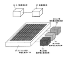
図1において、54は赤フィルタ部個別電圧値設定部、55は緑フィルタ部個別電圧値設定部、56は青フィルタ部個別電圧値設定部、57は画像撮像部、58はリーク画像検出部、59はカラーフィルタ付き有機EL表示パネル(有機ELパネル)である。54,55,56は個別電圧印加手段として機能し、57は画像撮像手段である。
In FIG. 1, 54 is a red filter unit individual voltage value setting unit, 55 is a green filter unit individual voltage value setting unit, 56 is a blue filter unit individual voltage value setting unit, 57 is an image pickup unit, 58 is a leak image detection unit, Reference numeral 59 denotes an organic EL display panel with a color filter (organic EL panel).
実施の形態1の検査工程では、まず、カラーフィルタ付き有機EL表示パネル59の電極に、赤フィルタ部個別電圧値設定部54と緑フィルタ部個別電圧値設定部55と青フィルタ部個別電圧値設定部56とを電気的に接続する。次に、赤フィルタ部個別電圧値設定部54と緑フィルタ部個別電圧値設定部55と青フィルタ部個別電圧値設定部56にて、カラーフィルタ付き有機EL表示パネル59の赤フィルタ部,緑フィルタ部,青フィルタ部のそれぞれに個別に電圧を印加する。
In the inspection process of the first embodiment, first, the red filter unit individual voltage value setting unit 54, the green filter unit individual voltage
この段階で、所定電圧、例えば、逆バイアス電圧を有機ELパネルに印加することにより、有機EL層に欠陥がある場合はリーク光が発生する。なお、カラーフィルタ毎の個別印加電圧値は、カラーフィルタ種別毎の基準リーク発光量が全種別で基準許容値内に入るよう設定されている。 At this stage, by applying a predetermined voltage, for example, a reverse bias voltage, to the organic EL panel, leak light is generated when the organic EL layer has a defect. The individual applied voltage value for each color filter is set so that the reference leak light emission amount for each color filter type falls within the reference allowable value for all types.
次に、画像撮像部57にてリーク光の画像を撮像する。そして、リーク画像検出部58でリーク不良を検出する。最終的な不良判断としては、ディスプレイなどに表示しての目視判定でもよいし、画像処理装置による自動判定でもよい。
Next, the
なお、本例では、赤フィルタ部個別電圧値設定部54,緑フィルタ部個別電圧値設定部55,青フィルタ部個別電圧値設定部56を個別にしているが、これらをまとめて一つにしてもよい。
In this example, the red filter unit individual voltage value setting unit 54, the green filter unit individual voltage
図2は実施の形態1における制御手段による有機ELパネル製造方法の検査工程のフローチャートである。 FIG. 2 is a flowchart of the inspection process of the organic EL panel manufacturing method by the control means in the first embodiment.
図2において、S1は電圧印加用電極接続のステップ、S2は赤フィルタ部個別電圧値印加指令のステップ、S3は緑フィルタ部個別電圧値印加指令のステップ、S4は青フィルタ部個別電圧値印加指令のステップ、S5は画像撮像部57への露光開始指令のステップ、S6は撮像手段への露光終了指令のステップ、S7はリーク光検出のステップ、S8は赤フィルタ部電圧解除指令のステップ、S9は緑フィルタ部電圧解除指令のステップ、S10は青フィルタ部電圧解除指令のステップ、S11は電圧印加用電極解除のステップである。
In FIG. 2, S1 is a voltage application electrode connection step, S2 is a red filter section individual voltage value application command step, S3 is a green filter section individual voltage value application command step, and S4 is a blue filter section individual voltage value application command. , S5 is an exposure start command step to the
本実施の形態1では、まず、電圧印加用電極接続のステップS1で有機ELパネルに電圧を印加するため、電極に印加用電源を接続する。次に、赤フィルタ部個別電圧値印加指令のステップS2で赤フィルタ部に赤フィルタ用の個別電圧値を印加し、緑フィルタ部個別電圧値印加指令のステップS3で緑フィルタ部に緑フィルタ用の個別電圧値を印加し、青フィルタ部個別電圧値印加指令のステップS4で青フィルタ部に青フィルタ用の個別電圧値を印加する。なお、本例では、赤,緑,青でステップを分けており、赤,緑,青の順番のフローにしているが、この範囲内で順番が変わってもよく、また同時に電圧印加してもよい。 In the first embodiment, first, in order to apply a voltage to the organic EL panel in step S1 of the voltage application electrode connection, an application power source is connected to the electrode. Next, an individual voltage value for a red filter is applied to the red filter unit at step S2 of the red filter unit individual voltage value application command, and a green filter unit is applied to the green filter unit at step S3 of the green filter unit individual voltage value application command. The individual voltage value is applied, and the individual voltage value for the blue filter is applied to the blue filter unit in step S4 of the blue filter unit individual voltage value application command. In this example, the steps are divided into red, green, and blue, and the flow is in the order of red, green, and blue. However, the order may change within this range, and voltage may be applied simultaneously. Good.
この段階で、所定電圧、例えば、逆バイアス電圧を有機ELパネルに印加することにより、有機EL層に欠陥がある場合はリーク光が発生する。次に、画像撮像部57への露光開始指令のステップS5で画像撮像部57での露光を開始し、画像撮像部57への露光終了指令のステップS6で画像撮像部57での露光を終了する。このステップS5,S6にてリーク光画像の撮像が実施される。
At this stage, by applying a predetermined voltage, for example, a reverse bias voltage, to the organic EL panel, leak light is generated when the organic EL layer has a defect. Next, exposure in the
そして、リーク光検出のステップS7でリーク光の検出を行う。ここでは、目視判定でもよいし、画像処理による自動判定でもよい。 Then, leak light is detected in step S7 of leak light detection. Here, visual determination or automatic determination by image processing may be used.
さらに、リーク光検出のステップS7は、画像撮像部57への露光終了指令のステップS6以降であれば、順序はどのステップでもよい。そして、赤フィルタ部電圧解除指令のステップS8、緑フィルタ部電圧解除指令のステップS9、青フィルタ部電圧解除指令のステップS10で有機ELパネルへの電圧印加を解除する。
Further, the order of the leak light detection step S7 may be any step as long as it is after step S6 of the exposure end command to the
なお、本例では、赤,緑,青でステップを分けており、赤,緑,青の順番にしているが、この範囲内で順番が変わってもよく、また、同時解除であってもよい。そして、電圧印加用電極解除のステップS11で電極から印加用電源を解除する。 In this example, the steps are divided into red, green, and blue, and the order is red, green, and blue. However, the order may be changed within this range, or simultaneous cancellation may be performed. . In step S11 for releasing the voltage application electrode, the application power source is released from the electrode.
次に、赤フィルタ部個別電圧値印加指令のステップS2と、緑フィルタ部個別電圧値印加指令のステップS3と、青フィルタ部個別電圧値印加指令のステップS4とにおける印加電圧値の設定について、図15と図18を参照して説明する。 Next, the setting of the applied voltage value in step S2 of the red filter unit individual voltage value application command, step S3 of the green filter unit individual voltage value application command, and step S4 of the blue filter unit individual voltage value application command will be described. 15 and FIG.
図15において、既述したように、赤フィルタ画素の事例で説明すると、ガラス基板401上の陽極101と陰極201に電源901で逆バイアス電圧を印加した際、電流リーク発生箇所601よりリーク発光701が発生し、赤カラーフィルタ501を通過した、赤カラーフィルタを通過したリーク発光801を観測することになる。
In FIG. 15, as described above, the case of the red filter pixel will be described. When a reverse bias voltage is applied to the
次に、仮に、陽極(赤フィルタ画素)101と陽極(緑フィルタ画素)102と陽極(青フィルタ画素)103とが同じで、陰極(赤フィルタ画素)201と陰極(緑フィルタ画素)202と陰極(青フィルタ画素)203とが同じで、有機EL層(赤フィルタ画素)301と有機EL層(緑フィルタ画素)302と有機EL層(青フィルタ画素)303が同じで、ガラス基板(赤フィルタ画素)401とガラス基板(緑フィルタ画素)402とガラス基板(青フィルタ画素)403が同じとする。 Next, assuming that the anode (red filter pixel) 101, the anode (green filter pixel) 102, and the anode (blue filter pixel) 103 are the same, the cathode (red filter pixel) 201, the cathode (green filter pixel) 202, and the cathode (Blue filter pixel) 203 is the same, organic EL layer (red filter pixel) 301, organic EL layer (green filter pixel) 302, and organic EL layer (blue filter pixel) 303 are the same, and a glass substrate (red filter pixel) ) 401, glass substrate (green filter pixel) 402, and glass substrate (blue filter pixel) 403 are the same.
さらに、電源(赤フィルタ画素)901,電源(緑フィルタ用画素)902,電源(青フィルタ画素)903により、同一電圧の逆バイアスを印加したときに、電流リーク発生箇所(赤フィルタ画素)601,電流リーク発生箇所(緑フィルタ画素)602,電流リーク発生箇所(青フィルタ画素)603から発生するリーク発光(赤フィルタ画素)701,リーク発光(緑フィルタ画素)702,リーク発光(青フィルタ画素)703の面積と強度が全く同一であり、かつ可視域の透過率が、赤カラーフィルタ501,緑カラーフィルタ502,青カラーフィルタ503の順で少なくなると仮定した場合、赤カラーフィルタ501を通過したリーク発光量(可視〜赤外波域)804,緑カラーフィルタ502を通過したリーク発光量(可視〜赤外波域)805,青カラーフィルタ503を通過したリーク発光量(可視〜赤外波域)806の順で、総発光量は少なくなる。
Further, when a reverse bias of the same voltage is applied by a power source (red filter pixel) 901, a power source (green filter pixel) 902, and a power source (blue filter pixel) 903, a current leak occurrence location (red filter pixel) 601 Current leak occurrence location (green filter pixel) 602, leak emission (red filter pixel) 701, leak emission (green filter pixel) 702, leak emission (blue filter pixel) 703 generated from current leak occurrence location (blue filter pixel) 603 Leaking light that has passed through the
図2の赤フィルタ部個別電圧値印加指令のステップS2、緑フィルタ部個別電圧値印加指令のステップS3、青フィルタ部個別電圧値印加指令のステップS4における印加電圧値の設定については、前記のようにリーク発光(赤フィルタ画素)701と、リーク発光(緑フィルタ画素)702と、リーク発光(青フィルタ画素)703の性質として、印加電圧によってリーク光強度が変わることを利用し、赤カラーフィルタ501を通過したリーク発光量(可視〜赤外波域)804、緑カラーフィルタ502を通過したリーク発光量(可視〜赤外波域)805、青カラーフィルタ503を通過したリーク発光量(可視〜赤外波域)806に応じた設定を行う。
The setting of the applied voltage value in step S2 of the red filter unit individual voltage value application command, step S3 of the green filter unit individual voltage value application command, and step S4 of the blue filter unit individual voltage value application command of FIG. 2 is as described above. The
具体的な印加電圧によるリーク光強度の変化であるが、逆バイアス印加の場合は、印加電圧が高くなるほど、リーク光強度が強くなる。したがって、図18の場合は、青>緑>赤の順で、青の電圧を一番高く、赤の電圧を一番低くすればよい。 This is a specific change in the leak light intensity due to the applied voltage. In the case of reverse bias application, the leak light intensity increases as the applied voltage increases. Therefore, in the case of FIG. 18, the blue voltage may be the highest and the red voltage may be the lowest in the order of blue> green> red.
このように、赤カラーフィルタ501を通過したリーク発光量(可視〜赤外波域)804と、緑カラーフィルタ502を通過したリーク発光量(可視〜赤外波域)805と、青カラーフィルタ503を通過したリーク発光量(可視〜赤外波域)806が等価となるよう、電圧値を調整することによって赤,緑,青を一括で撮像してリーク光の検出を行うことが可能となる。
As described above, the leak light emission amount (visible to infrared wave region) 804 that has passed through the
なお、等価の判断は、画像撮像した際に、基準となる赤カラーフィルタ501を通過したリーク発光量(可視〜赤外波域)804と、緑カラーフィルタ502を通過したリーク発光量(可視〜赤外波域)805と、青カラーフィルタ503を通過したリーク発光量(可視〜赤外波域)806の強度を定め、全ての強度が基準許容値内に入るよう設定することにより定量化が可能となる。
Note that the equivalent determination is based on the amount of leak light emission (visible to infrared wave region) 804 that has passed through the reference
具体的に、赤カラーフィルタ501を通過したリーク発光量(可視〜赤外波域)804,緑カラーフィルタ502を通過したリーク発光量(可視〜赤外波域)805,青カラーフィルタ503を通過したリーク発光量(可視〜赤外波域)806の強度が、どのように変化するのか、図3を参照しながら説明する。
Specifically, the amount of leak light emission (visible to infrared wave region) 804 that has passed through the
図3(a)〜(g)はカラーフィルタによるリーク光の変化を示す図であって、(a)は青カラーフィルタの透過特性例、(b)は緑カラーフィルタの透過特性例、(c)は赤カラーフィルタの透過特性例、(d)はリーク光の分光特性例、(e)は(a)の特性を有するカラーフィルタを透過した後のリーク光の分光特性、(f)は(b)の特性を有する緑カラーフィルタを透過した後のリーク光の分光特性、(g)は(c)の特性を有する赤カラーフィルタを透過した後のリーク光の分光特性である。 FIGS. 3A to 3G are diagrams showing changes in leakage light by the color filter, in which FIG. 3A is an example of transmission characteristics of a blue color filter, FIG. 3B is an example of transmission characteristics of a green color filter, and FIG. ) Is an example of transmission characteristics of a red color filter, (d) is an example of spectral characteristics of leakage light, (e) is spectral characteristics of leakage light after passing through a color filter having the characteristics of (a), and (f) is ( The spectral characteristic of the leaked light after passing through the green color filter having the characteristic b), and (g) is the spectral characteristic of the leaked light after passing through the red color filter having the characteristic of (c).
なお、図3では、概念説明を解りやすくするため、特性を直線的に模式化している。また(a),(b),(c)の縦軸は100%を最大値とした透過特性(透過率)、(d)の縦軸は100%を最大値とした強度、(e),(f),(g)の縦軸は(d)のリーク光強度の最大値を100%としたときの強度を示す。 In FIG. 3, the characteristics are linearly modeled for easy understanding of the concept description. The vertical axes of (a), (b), and (c) are transmission characteristics (transmittance) with a maximum value of 100%, the vertical axis of (d) is the intensity with a maximum value of 100%, (e), The vertical axes of (f) and (g) indicate the intensity when the maximum value of the leaked light intensity in (d) is 100%.
さらに、(e)には(a)の特性と(d)のリーク光強度も記載しており、(a)の特性を持つカラーフィルタを透過した後のリーク光の分光特性はハッチング部となる。計算式としては、各波長にて、〔(a)の透過率〕×〔(d)のリーク光強度〕=〔(e)のリーク光強度〕となる。同様に(f)には(b)の特性と(d)のリーク光強度も記載しており、(b)の特性を有するカラーフィルタを透過した後のリーク光の分光特性はハッチング部となる。計算式としては、各波長にて、〔(b)の透過率〕×〔(d)のリーク光強度〕=〔(f)のリーク光強度〕となり、同様に(g)には(c)の特性と(d)のリーク光強度も記載しており、(c)の特性を持つカラーフィルタを透過した後のリーク光の分光特性はハッチング部となる。計算式としては、各波長にて、〔(c)の透過率〕×〔(d)のリーク光強度〕=〔(g)のリーク光強度〕となる。 Furthermore, (e) also describes the characteristics of (a) and the leaked light intensity of (d), and the spectral characteristics of the leaked light after passing through the color filter having the characteristics of (a) is a hatched portion. . As a calculation formula, at each wavelength, [(a) transmittance] × [(d) leak light intensity] = [(e) leak light intensity]. Similarly, (f) also describes the characteristics of (b) and the leaked light intensity of (d), and the spectral characteristics of the leaked light after passing through the color filter having the characteristics of (b) is a hatched portion. . As a calculation formula, at each wavelength, [(transmittance of (b)] × [leakage light intensity of (d)] = [leakage light intensity of (f)]. Similarly, (g) includes (c) And the leakage light intensity of (d) are also described, and the spectral characteristic of the leakage light after passing through the color filter having the characteristic of (c) becomes a hatched portion. As a calculation formula, [(c) transmittance] × [(d) leak light intensity] = [(g) leak light intensity] at each wavelength.
このようにカラーフィルタの透過特性(透過率)とリーク光の分光特性により、図18に示すように、赤カラーフィルタ501を通過したリーク発光量(可視〜赤外波域)804と、緑カラーフィルタ502を通過したリーク発光量(可視〜赤外波域)805と、青カラーフィルタ503を通過したリーク発光量(可視〜赤外波域)806の強度が変化する。
Thus, due to the transmission characteristic (transmittance) of the color filter and the spectral characteristic of the leak light, as shown in FIG. 18, the amount of leak light emission (visible to infrared wave region) 804 that has passed through the
全ての波長において100%発光強度取得可能である撮像系であれば、(e)のハッチング部面積値が青カラーフィルタ503を通過したリーク発光量(可視〜赤外波域)806の強度、(f)のハッチング部面積値が緑カラーフィルタ502を通過したリーク発光量(可視〜赤外波域)805の強度、(g)のハッチング部面積値が赤カラーフィルタ501を通過したリーク発光量(可視〜赤外波域)804の強度リーク発光量強度となる。
If the imaging system is capable of acquiring 100% emission intensity at all wavelengths, the hatched area value of (e) is the intensity of the leaked light emission amount (visible to infrared wave region) 806 that has passed through the
なお、本例では赤,緑,青のカラーフィルタを例示したが、カラーフィルタは複数であれば、必ずしも、赤,緑,青である必要はない。また、カラーフィルタの特性とベースとなる有機EL素子の特性によっては、必ずしも、青の電圧を一番高く、赤の電圧を一番低くすればよいということではなく、これに限定されるものではない。 In this example, the red, green, and blue color filters are illustrated. However, as long as there are a plurality of color filters, it is not always necessary to use red, green, and blue. In addition, depending on the characteristics of the color filter and the characteristics of the organic EL element serving as the base, it is not always necessary to set the blue voltage to the highest and the red voltage to the lowest. Absent.
図3の説明では解りやすくするため、特性を直線的に模式化しているが、実際は直線的ではなく、カラーフィルタを例にとってみても、具体商品毎に状況は異なってくる。 In the description of FIG. 3, the characteristics are linearly modeled for easy understanding. However, in reality, the characteristics are not linear, and even if a color filter is taken as an example, the situation differs for each specific product.
ここで、赤カラーフィルタ501,緑カラーフィルタ502,青カラーフィルタ503の具体透過特性例を、液晶用カラーフィルタの例にして図16と図17とで説明したように、図16と図17での最大波長700nmで比較すると、図16(a)のトプティカル(登録商標)はG(緑カラーフィルタ)よりB(青カラーフィルタ)の透過率が大きく、図17のV−259−RGBでは、B(青カラーフィルタ)よりG(緑カラーフィルタ)の透過率が大きい。なお、どちらも700nmではR(赤カラーフィルタ)が、G(緑カラーフィルタ)およびB(青カラーフィルタ)より透過率が大きくなっている。このようにカラーフィルタの透過率に応じた設定が必要である。さらに撮像系も全ての波長において100%発光強度取得可能であるわけではなく、波長により量子効率が異なるため、適宜設定する必要がある。
Here, the specific transmission characteristic examples of the
以上のようにして検査を行った(検査手段での検査工程)後に、検査結果に基づいた必要な修正(修正手段での修正工程)を行うことで、有機ELパネルの製造を行う。例えば、検査結果によって、有機ELパネルの表示性能に対して影響しない程度の画素不良が有ることが分かった場合は、その有機EL画素が作用(機能)しないようにすることによって、有機ELパネルを製造することができる。また、ここで、修正が不要だと判断して修正を行わないことも修正手段での修正工程に含まれることは、言うまでもない。 After performing the inspection as described above (inspection process by the inspection means), the organic EL panel is manufactured by performing necessary correction (correction process by the correction means) based on the inspection result. For example, when it is found from the inspection result that there is a pixel defect that does not affect the display performance of the organic EL panel, the organic EL panel is made to prevent the organic EL pixel from acting (functioning). Can be manufactured. In addition, it goes without saying that it is included in the correcting step by the correcting means that it is determined that the correction is unnecessary and the correction is not performed.
(実施の形態2)
図4は本発明の実施の形態2における有機ELパネル製造装置の構成図であって、図1と同じ構成要素については同じ符号を用い、説明を省略する。
(Embodiment 2)
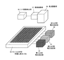
FIG. 4 is a block diagram of the organic EL panel manufacturing apparatus according to
図4において、60は赤フィルタ部電圧設定部、61は緑フィルタ部電圧値設定部、62は青フィルタ部電圧設定部、63はコントローラ部である。 In FIG. 4, 60 is a red filter section voltage setting section, 61 is a green filter section voltage value setting section, 62 is a blue filter section voltage setting section, and 63 is a controller section.
本実施の形態2の検査工程では、まず、カラーフィルタ付き有機EL表示パネル59の電極に、赤フィルタ部電圧設定部60と緑フィルタ部電圧設定部61と青フィルタ部電圧設定部62とを接続する。次に、赤フィルタ部電圧設定部60,緑フィルタ部電圧設定部61,青フィルタ部電圧設定部62にて、カラーフィルタ付き有機EL表示パネル59の赤フィルタ部,緑フィルタ部,青フィルタ部に電圧を印加する。この段階で、所定電圧、例えば、逆バイアス電圧を有機ELパネルに印加することにより、有機EL層に欠陥がある場合はリーク光が発生する。
In the inspection process of the second embodiment, first, a red filter unit
次に、コントローラ部63から画像撮像部57へリーク光の画像を撮像するに際し、露光開始の指令を出す。その後、コントローラ部63より、赤フィルタ部電圧設定部60,緑フィルタ部電圧設定部61,青フィルタ部電圧設定部62に順番で電圧印加解除の指令を出して電圧印加を解除する。そして、コントローラ部63より、画像撮像部57へ露光終了の指令を出す。このようにすることでリーク光画像の取得が完了する。
Next, when an image of leaked light is captured from the controller unit 63 to the
なお、カラーフィルタ毎の個別電圧印加時間はカラーフィルタ種別毎の基準リーク発光量とカラーフィルタ種別毎の電圧印加時間の積で計算される積算光量が全種別で基準許容値内に入るよう設定されていることで、基準リーク発光量が撮像された画像上にて全種別で等価となるように、コントローラ部63で制御されている。そして、リーク画像検出部58でリーク不良を検出する。ここは、ディスプレイなどに表示しての目視判定でもよいし、画像処理装置による自動判定でもよい。 The individual voltage application time for each color filter is set so that the integrated light amount calculated by the product of the reference leak emission amount for each color filter type and the voltage application time for each color filter type falls within the reference tolerance for all types. As a result, the controller unit 63 controls the reference leak light emission amount so as to be equivalent for all types on the captured image. The leak image detection unit 58 detects a leak failure. This may be a visual determination displayed on a display or the like, or an automatic determination by an image processing apparatus.
図5は本実施の形態2における有機ELパネル製造方法の検査工程のフローチャートである。図5において、図2と同じ構成要素については同じ符号を用いて説明を省略する。 FIG. 5 is a flowchart of the inspection process of the organic EL panel manufacturing method according to the second embodiment. In FIG. 5, the same components as those in FIG.
なお、図5には赤,緑,青のカラーフィルタが設けられた有機ELパネルを例示している。図5において、S12は赤フィルタ部電圧印加指令のステップ、S13は緑フィルタ部電圧印加指令のステップ、S14は青フィルタ部電圧印加指令のステップである。 FIG. 5 illustrates an organic EL panel provided with red, green, and blue color filters. In FIG. 5, S12 is a step of a red filter section voltage application command, S13 is a step of a green filter section voltage application command, and S14 is a step of a blue filter section voltage application command.
図5において、まず、電圧印加用電極接続のステップS1で有機ELパネルに電圧を印加するため、電極に印加用電源を接続する。次に、赤フィルタ部電圧印加指令のステップS12と、緑フィルタ部電圧印加指令のステップS13、青フィルタ部電圧印加指令のステップS14で有機ELパネルに電圧値を印加する。 In FIG. 5, first, in order to apply a voltage to the organic EL panel in step S1 of the voltage application electrode connection, an application power source is connected to the electrode. Next, a voltage value is applied to the organic EL panel in step S12 of the red filter unit voltage application command, step S13 of the green filter unit voltage application command, and step S14 of the blue filter unit voltage application command.
なお、本例では、赤,緑,青でステップを分けており、赤,緑,青の順番にしているが、この範囲内で順番が変わってもよく、また同時に電圧を印加してもよい。 In this example, the steps are divided into red, green, and blue, and the order is red, green, and blue. However, the order may be changed within this range, and a voltage may be applied simultaneously. .
この段階で、所定電圧、例えば、逆バイアス電圧を有機ELパネルに印加することで、有機EL層に欠陥がある場合はリーク光が発生する。次に、画像撮像部57への露光開始指令のステップS5で画像撮像部57の露光を開始する。そして、赤フィルタ部電圧解除指令のステップS8で赤フィルタ部への電圧供給を停止し、次に、緑フィルタ部電圧解除指令のステップS9で緑フィルタ部への電圧供給を停止し、次に、青フィルタ部電圧解除指令のステップS10で青フィルタ部への電圧供給を停止し、撮像手段への露光終了指令のステップS6で撮像手段での露光を終了する。このステップS8,S9,S10,S6でリーク光画像の撮像が実施される。このステップS8,S9,S10,S6のタイミングについては、後で詳しく説明する。
At this stage, by applying a predetermined voltage, for example, a reverse bias voltage, to the organic EL panel, leak light is generated when the organic EL layer has a defect. Next, exposure of the
そして、リーク光検出のステップS7でリーク光の検出を行う。最終判定は、目視判定でもよいし、画像処理による自動判定でもよい。さらに、リーク光検出のステップS7は、画像撮像部57への露光終了指令のステップS6以降であれば、順序はどのステップでもよい。そして、電圧印加用電極解除のステップS11で電極から印加用電源を解除する。
Then, leak light is detected in step S7 of leak light detection. The final determination may be visual determination or automatic determination by image processing. Further, the order of the leak light detection step S7 may be any step as long as it is after step S6 of the exposure end command to the
ステップS8,S9,S10,S6のタイミングについて図6を参照して説明する。 The timing of steps S8, S9, S10, and S6 will be described with reference to FIG.
図6は本実施の形態2におけるカメラ露光と電圧印加とのタイミングチャートであって、(a)はカメラ露光、(b)は赤フィルタ電圧印加、(c)は緑フィルタ電圧印加、(d)は青フィルタ電圧印加をそれぞれ示す。縦軸は電圧で横軸は時刻である。なお、図6に示す各部は既述した図15と図18と同様なものであることを前提としている。 FIG. 6 is a timing chart of camera exposure and voltage application in the second embodiment, where (a) is camera exposure, (b) is red filter voltage application, (c) is green filter voltage application, (d). Indicates the blue filter voltage application, respectively. The vertical axis represents voltage and the horizontal axis represents time. 6 is assumed to be the same as those shown in FIGS. 15 and 18 described above.
概略としては、図18の赤カラーフィルタ501を通過したリーク発光量(可視〜赤外波域)804、緑カラーフィルタ502を通過したリーク発光量(可視〜赤外波域)805、青カラーフィルタ503を通過したリーク発光量(可視〜赤外波域)806が、赤,緑,青の順で少なくなる場合は、図6のTVR<TVG<TVBの順で、TVRを最も短く、TVBを最も長く設定すればよい。
As outline, the amount of leak light emission (visible to infrared wave region) 804 that has passed through the
具体的には、カラーフィルタを通過したリーク発光量(可視〜赤外波域)804、緑カラーフィルタを通過したリーク発光量(可視〜赤外波域)805、青カラーフィルタを通過したリーク発光量(可視〜赤外波域)806と、カラーフィルタ種別毎の電圧印加時間と、図6のTVR,TVG,TVBとの、それぞれの積で計算される積算光量が全種別で基準許容値内に入ることで等価となるように設定を行う。 Specifically, the amount of leak light emitted through the color filter (visible to infrared wave region) 804, the amount of leak light emitted through the green color filter (visible to infrared wave region) 805, and the amount of leak light emitted through the blue color filter The total amount of light calculated by the product of the amount (visible to infrared wave region) 806, the voltage application time for each color filter type, and TVR, TVG, TVB in FIG. Set to be equivalent by entering.
なお、露光タイミング(カメラ露光TC)は、青フィルタ部電圧解除指令のステップS10で青フィルタ部への電圧供給を停止した直後に、画像撮像部57への露光終了指令のステップS6で画像撮像部57での露光を終了していればよく、TC>=TVB(厳密にはTCの立ち上がりとTVBの立ち上がりが同時であるとの前提がある)であればよい。このように、カラーフィルタを通過したリーク発光量(可視〜赤外波域)804,緑カラーフィルタを通過したリーク発光量(可視〜赤外波域)805,青カラーフィルタを通過したリーク発光量(可視〜赤外波域)806と、TVR,TVG,TVBとのそれぞれの積で計算される積算光量が赤,緑,青の各フィルタで等価となるように、TVR,TVG,TVB,TCを調整することにより、赤,緑,青を一括で撮像し検出を行うことが可能となる。
The exposure timing (camera exposure TC) is determined immediately after the voltage supply to the blue filter unit is stopped in step S10 of the blue filter unit voltage release command, and in step S6 of the exposure end command to the
(実施の形態3)
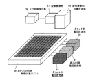
図7は本発明の実施の形態3における有機EL製造装置の構成図であって、図5において、図1,図3と同じ構成要素については同じ符号を用い、その説明を省略する。なお、図5において、64は焦点調整部である。
(Embodiment 3)
FIG. 7 is a block diagram of an organic EL manufacturing apparatus according to
本実施の形態3の検査工程では、まず、カラーフィルタ付き有機EL表示パネル59の電極に、赤フィルタ部電圧設定部60と緑フィルタ部電圧設定部61と青フィルタ部電圧設定部62とを接続する。次に、赤フィルタ部電圧設定部60にて、カラーフィルタ付き有機EL表示パネル59の赤フィルタ部に電圧を印加する。この段階で、所定電圧、例えば、逆バイアス電圧を有機ELパネルに印加することにより、赤フィルタ部の有機EL層に欠陥がある場合はリーク光が発生する。
In the inspection process of the third embodiment, first, the red filter unit
焦点調整部64において、画像撮像部57を制御するか有機EL表示パネル59を移動させることにより、画像撮像部57とカラーフィルタ付き有機EL表示パネル59の焦点を調整する。この制御は画像撮像部57全体を移動させてもよいし、画像撮像部57内部の光学系の一部を移動させてもよい。次に、画像撮像部57にて、リーク光の画像を撮像する。そして、リーク画像検出部58でリーク不良を検出する。最終判定は、ディスプレイなどに表示しての目視判定でもよいし、画像処理装置による自動判定でもよい。これで赤フィルタ部の検出処理は終了し、同様に緑フィルタ部と青フィルタ部についても処理を行う。
In the focus adjustment unit 64, the focus of the
図8は本実施の形態3における有機ELパネル製造方法の検査工程のフローチャートであって、図2,図5と同様のステップについては同じ符号を用い、その説明を省略する。 FIG. 8 is a flowchart of the inspection process of the organic EL panel manufacturing method according to the third embodiment. The same steps as those in FIGS. 2 and 5 are denoted by the same reference numerals, and the description thereof is omitted.
なお、図8において、赤、緑、青のカラーフィルタがついた有機ELパネルを例示し、S15は赤フィルタ部位置移動指令のステップ、S16は緑フィルタ部位置移動指令のステップ、S17は青フィルタ部位置移動指令のステップである。 8 exemplifies an organic EL panel with red, green, and blue color filters. S15 is a step of a red filter portion position movement command, S16 is a step of a green filter portion position movement command, and S17 is a blue filter. This is a step of a part position movement command.
図8において、まず、電圧印加用電極接続のステップS1で有機ELパネルに電圧を印加するため、電極に印加用電源を接続する。次に、赤フィルタ部電圧印加指令のステップS12で有機ELパネルに電圧値を印加する。そして、赤フィルタ位置移動指令のステップS15で赤フィルタ用のリーク発光位置を最適な状態で撮像するために、有機ELパネルと画像撮像部57の撮像素子との位置関係を最適な位置に移動させる。
In FIG. 8, first, in order to apply a voltage to the organic EL panel in step S1 of the voltage application electrode connection, an application power source is connected to the electrode. Next, a voltage value is applied to the organic EL panel in step S12 of the red filter section voltage application command. In step S15 of the red filter position movement command, the positional relationship between the organic EL panel and the image pickup device of the
次に、画像撮像部57への露光開始指令のステップS5で画像撮像部57での露光を開始し、画像撮像部57への露光終了指令のステップS6で画像撮像部57での露光を終了する。このステップS5,S6で赤フィルタ部のリーク光画像の撮像が実施される。そして、リーク光検出のステップS7でリーク光の検出を行う。最終判定は、目視判定でもよいし、画像処理による自動判定でもよい。そして、赤フィルタ部電圧解除指令のステップS8で電圧を解除する。
Next, exposure in the
次に、緑フィルタについて、ステップS13,S16,S5,S6,S7,S9の順で、赤フィルタの場合と同様の処理を行い、さらに、青フィルタについて、ステップS14,S17,S5,S6,S7,S10の順で処理を行い、電圧印加用電極解除のステップS11で電極から印加用電源を解除する。ここで、赤,緑,青の各フィルタの処理は、必ずしもこの順番でなくてもよいし、電圧印加と解除も、画像撮像時に電圧が印加されていればよく、赤,緑,青の各フィルタが同時でもよい。さらにリーク光検出は、赤,緑,青の画像を、それぞれ赤,緑,青が解るように記憶しておけば、その順番は変えてもよい。 Next, the green filter is processed in the order of steps S13, S16, S5, S6, S7, and S9 in the order of the red filter, and the blue filter is further processed in steps S14, S17, S5, S6, and S7. , S10 in this order, and the power supply for application is released from the electrode in step S11 of the electrode release for voltage application. Here, the processing of each filter of red, green, and blue does not necessarily need to be performed in this order, and voltage application and release may be performed only when a voltage is applied at the time of image capture, and each of red, green, and blue is processed. The filters may be simultaneous. Furthermore, the leak light detection may be changed in order to store red, green, and blue images so that red, green, and blue can be understood.
次に、赤フィルタ部位置移動指令のステップS15、緑フィルタ部位置移動指令のステップS16、青フィルタ部位置移動指令のステップS17での位置の設定について、図15,図18を参照して説明する。 Next, setting of the position in step S15 of the red filter unit position movement command, step S16 of the green filter unit position movement command, and step S17 of the blue filter unit position movement command will be described with reference to FIGS. .
仮に、図15のリーク発光(赤フィルタ画素)701と、リーク発光(緑フィルタ画素)702と、リーク発光(青フィルタ画素)703とが全く同じスペクトルで全く同じ強度であるとして、赤カラーフィルタ501,緑カラーフィルタ502,青カラーフィルタ503で赤外線波長域の透過率が同じと仮定し、可視域の透過率が、赤カラーフィルタ501,緑カラーフィルタ502,青カラーフィルタ503の順で少なくなると仮定した場合、図18に示すように、赤カラーフィルタを通過したリーク発光量(可視〜赤外波域)804、緑カラーフィルタを通過したリーク発光量(可視〜赤外波域)805、青カラーフィルタを通過したリーク発光量(可視〜赤外波域)806の順で、総発光量は少なくなるが、赤カラーフィルタを通過したリーク発光量(赤外波長域)807,緑カラーフィルタを通過したリーク発光量(赤外波長域)808,青カラーフィルタを通過したリーク発光量(赤外波長域)809の光量は同じである。
Assuming that the leak light emission (red filter pixel) 701, the leak light emission (green filter pixel) 702, and the leak light emission (blue filter pixel) 703 in FIG. 15 have exactly the same spectrum and the same intensity, the
この場合、図15の赤カラーフィルタ501を通過したリーク光801、緑カラーフィルタ502を通過したリーク光802、青カラーフィルタ503を通過したリーク光803における赤外線成分の含まれる量の割合が相対的に変わってくる。したがって、可視と近赤外の色収差によって、赤カラーフィルタ501を通過したリーク光801、緑カラーフィルタ502を通過したリーク光802、青カラーフィルタ503を通過したリーク光803に対する画像撮像部57の焦点位置はそれぞれ異なってくる。よって、それぞれのフィルタ毎で最も焦点の合う位置に移動させる必要がある。
In this case, the ratio of the amount of the infrared component contained in the
なお、画像撮像部57の焦点に関して、画像撮像部57内の光学系色収差が問題となることがある。それに対しては、レンズの材料に蛍石のような色収差の少ないものを使って、レンズと撮像素子の組み合わせもできるだけ収差を少なくするなどによって、色収差の影響を少なくすることはできる。
Note that the chromatic aberration of the optical system in the
しかし、レンズの収差ゼロは基本的にあり得ない。収差が許容範囲内であるか否かの問題である。収差の表れ方は、画像を撮像する際の画面中心と画面端、またはレンズの絞りなどで変わってくる。例えば、画面中央は位置補正不要だが、画面端の場合のみ補正するなどの使い方があってもよい。 However, there is basically no lens aberration. The problem is whether the aberration is within an acceptable range. The manner in which the aberration appears varies depending on the center of the screen and the edge of the screen when the image is taken, or the aperture of the lens. For example, the center of the screen does not require position correction, but it may be used only for correction at the edge of the screen.
なお、蛍石は高価でありコストの問題がある。加えて、検査対象が特に大型ディスプレイである場合は、画像撮像部57の画素数を大きくして検査したい、また撮像素子サイズをできるだけ大きくして量子効率を上げ、感度を上げて高速検査したいなどの要望がある。その場合、レンズには、大きなイメージサークルが要求される。その場合は、収差補正の難易度は非常に高くなり、レンズもが大型化し、コスト的にはさらに厳しくなってしまう。このような場合でも、本実施の形態による焦点補正による色収差補正より、イメージサークルを優先するレンズを使用することが可能になる。
Fluorite is expensive and has a problem of cost. In addition, when the inspection target is a particularly large display, it is desired to perform inspection by increasing the number of pixels of the
(実施の形態4)
図9は本発明の実施の形態4における有機ELパネル製造装置の構成図であって、図1,図4,図7と同じ構成要素については同じ符号を用い、その説明を省略する。なお、図9において、65は画像撮像部位置設定部である。
(Embodiment 4)
FIG. 9 is a block diagram of an organic EL panel manufacturing apparatus according to
本実施の形態4の検査工程では、まず、カラーフィルタ付き有機EL表示パネル59の電極に、赤フィルタ部電圧設定部60と緑フィルタ部電圧設定部61と青フィルタ部電圧設定部62とを接続する。次に、赤フィルタ部電圧設定部60と緑フィルタ部電圧設定部61と青フィルタ部電圧設定部62にて、カラーフィルタ付き有機EL表示パネル59の赤フィルタ部,緑フィルタ部,青フィルタ部のそれぞれに個別に電圧を印加する。この段階で、所定電圧、例えば、逆バイアス電圧を有機ELパネルに印加することにより、有機EL層に欠陥がある場合はリーク光が発生する。
In the inspection process of the fourth embodiment, first, the red filter unit
次に、画像撮像部位置設定部65にて、画像撮像部57を制御するか有機EL表示パネル59を移動させることにより、画像撮像部57とカラーフィルタ付き有機EL表示パネル59の焦点が最適となるように設定を行う。なお、この動作は、画像撮像部57にて、リーク光の画像を撮像する前までに終了していればよい。次に、画像撮像部57にて、リーク光の画像を撮像する。そして、リーク画像検出部58でリーク不良を検出する。最終判定は、ディスプレイなどに表示しての目視判定でもよいし、画像処理装置による自動判定でもよい。
Next, the image pickup unit
図10は本実施の形態4における有機EL製造方法の検査工程のフローチャートであって、図2,図5,図8と同様のステップについては同じ符号を用い、その説明を省略する。なお、図8において、赤,緑,青のカラーフィルタが設けられた有機ELパネルを例示し、S18は画像撮像部57への位置移動指令のステップである。
FIG. 10 is a flowchart of the inspection process of the organic EL manufacturing method according to the fourth embodiment. The same steps as those in FIGS. 2, 5, and 8 are denoted by the same reference numerals, and the description thereof is omitted. In FIG. 8, an organic EL panel provided with red, green, and blue color filters is illustrated, and S18 is a step of a position movement command to the
図10において、まず、電圧印加用電極接続のステップS1で有機ELパネルに電圧を印加するため、電極に印加用電源を接続する。次に、赤フィルタ部個別電圧値印加指令のステップS2で赤フィルタ部に赤フィルタ用の個別電圧値を印加し、緑フィルタ部個別電圧値印加指令のステップS3で緑フィルタ部に緑フィルタ用の個別電圧値を印加し、青フィルタ部個別電圧値印加指令のステップS4で青フィルタ部に青フィルタ用の個別電圧値を印加する。なお、ここでは、赤,緑,青のフィルタ部毎でステップを分けており、赤,緑,青の順番にしているが、この範囲内で順番が変わってもよく、また同時印加でもよい。 In FIG. 10, first, in order to apply a voltage to the organic EL panel in step S1 of the voltage application electrode connection, an application power source is connected to the electrode. Next, an individual voltage value for a red filter is applied to the red filter unit at step S2 of the red filter unit individual voltage value application command, and a green filter unit is applied to the green filter unit at step S3 of the green filter unit individual voltage value application command. The individual voltage value is applied, and the individual voltage value for the blue filter is applied to the blue filter unit in step S4 of the blue filter unit individual voltage value application command. Here, the steps are divided for each of the red, green, and blue filter units, and the order is red, green, and blue. However, the order may be changed within this range, or simultaneous application may be performed.
この段階で、所定電圧、例えば、逆バイアス電圧を有機ELパネルに印加することで、有機EL層に欠陥がある場合はリーク光が発生する。次に、画像撮像部57への位置移動指令のステップS18で、カラーフィルタ種別毎の基準リーク発光焦点位置との相対距離が最短になる焦点位置に移動する。このステップについては、後に、別途説明する。
At this stage, by applying a predetermined voltage, for example, a reverse bias voltage, to the organic EL panel, leak light is generated when the organic EL layer has a defect. Next, in step S18 of the position movement command to the
次に、画像撮像部57への露光開始指令のステップS5で画像撮像部57での露光を開始し、画像撮像部57への露光終了指令のステップS6で画像撮像部57での露光を終了する。このステップS5,S6でリーク光画像の撮像が実施される。そして、リーク光検出のステップS7でリーク光の検出を行う。最終判定は、目視判定でもよいし、画像処理による自動判定でもよい。さらに、リーク光検出のステップS7は、画像撮像部57への露光終了指令のステップS6以降であれば、順序はどこでもよい。
Next, exposure in the
そして、赤フィルタ部電圧解除指令のステップS8、緑フィルタ部電圧解除指令のステップS9、青フィルタ部電圧解除指令のステップS10で有機ELパネルへの電圧印加を解除する。なお本例では、赤,緑,青の各フィルタでステップを分けており、赤,緑,青の順番にしているが、この範囲内で順番が変わってもよく、また同時解除でもよい。そして、電圧印加用電極解除のステップS11で電極から印加用電源を解除する。 Then, the voltage application to the organic EL panel is canceled in step S8 of the red filter section voltage release command, step S9 of the green filter section voltage release command, and step S10 of the blue filter section voltage release command. In this example, the steps are divided by the red, green, and blue filters, and the steps are in the order of red, green, and blue. However, the order may change within this range, or simultaneous cancellation may be performed. In step S11 for releasing the voltage application electrode, the application power source is released from the electrode.
なお、画像撮像部57への位置移動指令のステップS18での位置の設定であるが、図15の可視と近赤外の色収差によって赤カラーフィルタ501を通過したリーク光801,緑カラーフィルタ502を通過したリーク光802,青カラーフィルタ503を通過したリーク光803に対する画像撮像部57の焦点位置はそれぞれ異なってくる。従って、赤,緑,青の各フィルタで、最も焦点の合う位置、具体的には赤,青,緑のリーク発光焦点基準位置をあらかじめ求めておき、カラーフィルタ種別毎の基準リーク発光焦点位置との相対距離が最短になる焦点位置にすればよい。
The position setting in step S18 of the position movement command to the
なお、前記の通り、収差の表れ方は、画像を撮像する際の画面中心と画面端、またはレンズの絞りなどで変わるため、具体的にはレンズの絞りを通常の検出よりも開き、できるだけ画面端で焦点を合わせて補正するなどの使い方が好ましい。加えて、製造対象である有機ELパネルの機種により焦点の状況は変わってくるため、同一機種では位置は同じであるが、機種毎に位置を移動させるなどの使い方があってもよい。 Note that, as described above, the manner in which the aberration appears varies depending on the screen center and the edge of the image when capturing an image, or the lens aperture, and so on. It is preferable to use a correction method such as focusing at the end. In addition, since the focus state varies depending on the model of the organic EL panel to be manufactured, the position is the same in the same model, but there may be a method of moving the position for each model.
さらに図10のシーケンスは、図11のように変更してもよい。図11のフローでは、実施の形態2における有機ELパネル製造方法のフローチャートと同様に、フィルタ種別毎に電圧印加タイミングを変えるようにしている。 Further, the sequence of FIG. 10 may be changed as shown in FIG. In the flow of FIG. 11, the voltage application timing is changed for each filter type, as in the flowchart of the organic EL panel manufacturing method in the second embodiment.
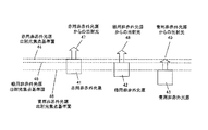
(実施の形態5)
図12は本発明の実施の形態5における有機EL製造装置における要部の説明図であって、29は赤フィルタ、30は緑フィルタ、31は青フィルタ、32は赤用光源、33は緑用光源、34は青用光源、35は赤用光源からの出射光、36は緑用光源からの出射光、37は青用光源からの出射光、38は赤フィルタを通過した赤用光源からの出射光、39は緑フィルタを通過した緑用光源からの出射光、40は青フィルタを通過した青用光源からの出射光である。
(Embodiment 5)
FIG. 12 is an explanatory diagram of a main part of the organic EL manufacturing apparatus according to
本実施の形態5おいて、赤フィルタ29を通過した赤用光源32からの出射光38と、緑フィルタ30を通過した緑用光源33からの出射光39と、青フィルタ31を通過した青用光源34からの出射光40の発光量の比は、製造対象であるカラーフィルタ付き有機ELパネルなどから発せられてカラーフィルタ越しに測定したフィルタ種別毎のリーク光の光量比が基準許容値内に入るようにすることにより、等価に設定され、リーク光検出を行う際の基準となるリーク光を発生させるために使用する。
In the fifth embodiment, the emitted light 38 from the red light source 32 that has passed through the red filter 29, the emitted light 39 from the green light source 33 that has passed through the
本来では、有機ELリーク光そのものが使えればよいが、有機ELリーク光は経時変化があり、安定した基準としては使いにくい面がある。したがって、経時変化の要素を取り除くために、赤用光源32と緑用光源33と青用光源34は、有機EL不良リークの発光と異なる発光状態のものとする。よって、製造対象であるカラーフィルタ付き有機ELパネルなどから発せられるリーク光と校正を取る必要がある。 Originally, the organic EL leak light itself may be used, but the organic EL leak light changes with time, and is difficult to use as a stable reference. Therefore, in order to remove the element of change over time, the red light source 32, the green light source 33, and the blue light source 34 are assumed to have a light emission state different from the light emission of the organic EL defect leak. Therefore, it is necessary to calibrate with leakage light emitted from an organic EL panel with a color filter, which is a manufacturing target.
また、リーク光は微弱かつ微小であるため、例えば、赤フィルタ29と赤用光源32の間に、減光フィルタやピンホールなどを入れて大きさや強度を調整してもよいし、LEDなどの微小な光源を用いて電気的に強度を変えるなどの手段を取ってもよい。 In addition, since the leak light is weak and minute, for example, the size and intensity may be adjusted by inserting a neutral density filter, a pinhole or the like between the red filter 29 and the red light source 32. You may take means, such as changing intensity | strength electrically using a micro light source.
(実施の形態6)
図13は本発明の実施の形態6における有機ELパネル製造装置における要部の説明図であって、41は赤用非赤外光源、42は緑用非赤外光源、43は青用非赤外光源、44は赤用非赤外光源出射光焦点基準面、45は緑用非赤外光源出射光焦点基準面、46は青用非赤外光源出射光焦点基準面、47は赤用非赤外光源からの出射光、48は緑用非赤外光源からの出射光、49は青用非赤外光源からの出射光である。
(Embodiment 6)
FIG. 13 is an explanatory diagram of the main part of the organic EL panel manufacturing apparatus according to
本実施の形態6は、赤外線波長を含まない各光源41〜43の高さが、製造対象である複数のカラーフィルタ付き有機ELパネルにおけるカラーフィルタ種別毎のリーク発光焦点位置に対応した高さに個別で設定されている。
In the sixth embodiment, the height of each of the
前記のように有機ELリーク光は経時変化があり、安定した基準としては使いにくい面がある。したがって、経時変化の要素を取り除くために、有機EL不良リークの発光とは別方式の発光手段を用いる必要がある。 As described above, the organic EL leak light changes with time, and is difficult to use as a stable reference. Therefore, it is necessary to use a light emitting means of a method different from the light emission of the organic EL defect leakage in order to remove the element of change with time.
このとき、有機EL不良リーク発光と全く同じスペクトルが生成できればよいが、それは非常に難しい。よって、あいまいな赤外成分を取り除き、赤外成分の影響を高さそのものに変換することによって、焦点位置の基準を簡単に生成することができる。したがって、赤用非赤外光源41,緑用非赤外光源42,青用非赤外光源43からは、赤外成分を含まない出射光47,出射光48,出射光49がそれぞれ出射されており、赤用非赤外光源出射光焦点基準面44と、緑用非赤外光源出射光焦点基準面45と、青用非赤外光源出射光焦点基準面46は、製造対象である複数のカラーフィルタ付き有機ELパネルにおけるカラーフィルタ種別毎のリーク発光焦点位置に対応した相対高さに個別で設定されている。
At this time, it is sufficient that the same spectrum as the organic EL defective leak emission can be generated, but it is very difficult. Therefore, the reference of the focal position can be easily generated by removing the ambiguous infrared component and converting the influence of the infrared component into the height itself. Therefore, from the non-infrared
本発明は、カラーフィルタを有する有機ELパネルであっても、フィルタ種別毎の強度や焦点の違いを補正してリーク発光を検出することにより、高速高精度に有機EL膜不良の検出を行うことができるため、有機ELパネルの利用拡大に伴う製造装置のコストダウンや、有機ELパネルの大型化に伴う検出の高速化の要求などに対応でき、具体的には、有機EL素子、あるいは有機EL素子からなる有機ELパネルの画素に生じる電気的リーク不良位置や、有機EL素子を構成する陽極,EL発光部,陰極などの膜厚バラつきや、各構成部の界面不具合,有機EL層の劣化など、有機EL素子あるいは有機ELパネルの画素に生じる欠陥の検査工程に適用される。 Even if an organic EL panel having a color filter is used in the present invention, it is possible to detect organic EL film defects at high speed and high accuracy by detecting leakage light emission by correcting differences in intensity and focus for each filter type. Therefore, it can respond to the cost reduction of the manufacturing equipment accompanying the expansion of the use of the organic EL panel and the demand for high-speed detection accompanying the enlargement of the organic EL panel. Specifically, the organic EL element or the organic EL Locations of defective electrical leaks that occur in pixels of organic EL panels composed of elements, variations in film thicknesses of anodes, EL light emitting parts, cathodes, etc. constituting organic EL elements, interface defects in each constituent part, deterioration of organic EL layers, etc. The present invention is applied to an inspection process for defects generated in pixels of an organic EL element or an organic EL panel.
19 陽極
20 陰極
21 有機EL層
22 基板
23 凹凸部もしくは異物
24 電源
25 リーク光
26 表示パネル
27 表示部
28 ダミー有機EL発光部
29 赤フィルタ
30 緑フィルタ
31 青フィルタ
32 赤用光源
33 緑用光源
34 青用光源
35 赤用光源
36 緑用光源からの出射光
37 青用光源からの出射光
38 赤フィルタを通過した赤用光源からの出射光
39 緑フィルタを通過した緑用光源からの出射光
40 青フィルタを通過した青用光源からの出射光
41 赤用非赤外光源
42 緑用非赤外光源
43 青用非赤外光源
44 赤用非赤外光源出射光焦点基準面
45 緑用非赤外光源出射光焦点基準面
46 青用非赤外光源出射光焦点基準面
47 赤用非赤外光源からの出射光
48 緑用非赤外光源からの出射光
49 青用非赤外光源からの出射光
54 赤フィルタ部個別電圧値設定部
55 緑フィルタ部個別電圧値設定部
56 青フィルタ部個別電圧値設定部
57 画像撮像部
58 リーク画像検出部
59 カラーフィルタ付き有機EL表示パネル
60 赤フィルタ部電圧設定部
61 緑フィルタ部電圧値設定部
62 青フィルタ部電圧設定部
63 コントローラ部
64 焦点調整部
65 画像撮像部位置設定部
100 陽極
101 陽極(赤フィルタ)
102 陽極(緑フィルタ)
103 陽極(青フィルタ)
110 正孔
200 陰極
201 陰極(赤フィルタ)
202 陰極(緑フィルタ)
203 陰極(青フィルタ)
210 電子
300 有機EL層
301 有機EL層(赤フィルタ)
302 有機EL層(緑フィルタ)
303 有機EL層(青フィルタ)
309 異物
400 ガラス基板
401 ガラス基板(赤フィルタ)
402 ガラス基板(緑フィルタ)
403 ガラス基板(青フィルタ)
500 カラーフィルタ
501 赤カラーフィルタ
502 緑カラーフィルタ
503 青カラーフィルタ
601 電流リーク発生箇所(赤フィルタ)
602 電流リーク発生箇所(緑フィルタ)
603 電流リーク発生箇所(青フィルタ)
701 リーク発光(赤フィルタ)
702 リーク発光(緑フィルタ)
703 リーク発光(青フィルタ)
801 赤カラーフィルタを通過したリーク発光
802 緑カラーフィルタを通過したリーク発光
803 青カラーフィルタを通過したリーク発光
804 赤カラーフィルタを通過したリーク発光量(可視〜赤外波長域)
805 緑カラーフィルタを通過したリーク発光量(可視〜赤外波長域)
806 青カラーフィルタを通過したリーク発光量(可視〜赤外波長域)
807 赤カラーフィルタを通過したリーク発光量(赤外波長域)
808 緑カラーフィルタを通過したリーク発光量(赤外波長域)
809 青カラーフィルタを通過したリーク発光量(赤外波長域)
901 電源(赤フィルタ)
902 電源(緑フィルタ)
903 電源(青フィルタ)
1000 微弱光検出カメラ
1100 レンズ
19 Anode 20 Cathode 21 Organic EL layer 22 Substrate 23 Concavity and convexity or foreign matter 24 Power supply 25 Leakage light 26 Display panel 27 Display unit 28 Dummy organic EL light emitting unit 29 Red filter 30 Green filter 31 Blue filter 32 Red light source 33 Green light source 34 Light source for blue 35 Light source for red 36 Light emitted from light source for green 37 Light emitted from light source for blue 38 Light emitted from light source for red passing through red filter 39 Light emitted from light source for green passing through green filter 40 Light emitted from the blue light source that has passed through the blue filter 41 Non-infrared light source for red 42 Non-infrared light source for green 43 Non-infrared light source for blue 44 Non-infrared light source for red Output focus reference plane 45 Non-red for green Outgoing light source focus reference surface 46 Blue non-infrared light source output light focus reference surface 47 Outgoing light from red non-infrared light source 48 Outgoing light from green non-infrared light source 49 From blue non-infrared light source Outgoing light 5 4 Red filter section individual voltage value setting section 55 Green filter section individual voltage value setting section 56 Blue filter section individual voltage value setting section 57 Image capturing section 58 Leakage image detection section 59 Organic EL display panel with color filter 60 Red filter section voltage setting Unit 61 green filter unit voltage value setting unit 62 blue filter unit voltage setting unit 63 controller unit 64 focus adjustment unit 65 image imaging unit position setting unit 100 anode 101 anode (red filter)
102 Anode (green filter)
103 Anode (blue filter)
110
202 Cathode (green filter)
203 Cathode (blue filter)
210 Electronic 300
302 Organic EL layer (green filter)
303 Organic EL layer (blue filter)
309
402 Glass substrate (green filter)
403 Glass substrate (blue filter)
500
602 Location of current leak (green filter)
603 Location of current leak (blue filter)
701 Leak emission (red filter)
702 Leakage emission (green filter)
703 Leak emission (blue filter)
801
805 Leakage emission amount that passed through the green color filter (visible to infrared wavelength range)
806 Amount of leaked light that has passed through the blue color filter (visible to infrared wavelength range)
807 Amount of light emitted through the red color filter (infrared wavelength region)
808 Amount of leaked light that passed through the green color filter (infrared wavelength region)
809 Amount of leaked light that passed through the blue color filter (infrared wavelength region)
901 Power supply (red filter)
902 Power supply (green filter)
903 Power supply (blue filter)
1000 Weak
Claims (8)
前記カラーフィルタの種別毎のリーク発光量が全種別において基準許容値内に入るように調整した後に、前記有機ELパネルからのリーク光に基づいて前記有機ELパネルの検査を行う検査工程と、
前記検査工程の検査結果に基づいた修正を前記有機ELパネルに行う修正工程と、を有することを特徴とする有機ELパネル製造方法。 For an organic EL panel provided with a plurality of types of color filters, after adjusting the amount of leak light emission for each type of the color filter by applying a predetermined voltage to be within a standard allowable value in all types, the organic EL panel An inspection process for inspecting the organic EL panel based on leaked light from
And a correction step of performing correction on the organic EL panel based on the inspection result of the inspection step.
前記個別電圧印加手段により前記カラーフィルタ毎に個別に印加される印加電圧値を、前記カラーフィルタの種別毎のリーク発光量が全種別で基準許容値内に入るように設定し、前記有機ELパネルからのリーク発光量が全種別で基準許容値内に入るように制御して、前記有機ELパネルの検査を行う検査手段と、
前記検査手段での検査結果に基づいて前記有機ELパネルの修正を行う修正手段と、を備えたことを特徴とする有機ELパネル製造装置。 Individual voltage application means for individually applying a predetermined voltage to an organic EL panel provided with a plurality of types of color filters;
An applied voltage value individually applied to each color filter by the individual voltage applying unit is set so that a leak light emission amount for each type of the color filter falls within a reference allowable value for all types, and the organic EL panel Control means for inspecting the organic EL panel by controlling so that the amount of leaked light emission from within the standard allowable value in all types,
An organic EL panel manufacturing apparatus, comprising: correction means for correcting the organic EL panel based on the inspection result of the inspection means.
Priority Applications (2)
| Application Number | Priority Date | Filing Date | Title |
|---|---|---|---|
| JP2008168689A JP5228649B2 (en) | 2008-06-27 | 2008-06-27 | Organic EL panel manufacturing method and manufacturing apparatus |
| US12/492,455 US7874888B2 (en) | 2008-06-27 | 2009-06-26 | Inspection method and inspection device, repairing method and repairing device for organic electroluminescence panel |
Applications Claiming Priority (1)
| Application Number | Priority Date | Filing Date | Title |
|---|---|---|---|
| JP2008168689A JP5228649B2 (en) | 2008-06-27 | 2008-06-27 | Organic EL panel manufacturing method and manufacturing apparatus |
Publications (2)
| Publication Number | Publication Date |
|---|---|
| JP2010009964A true JP2010009964A (en) | 2010-01-14 |
| JP5228649B2 JP5228649B2 (en) | 2013-07-03 |
Family
ID=41448007
Family Applications (1)
| Application Number | Title | Priority Date | Filing Date |
|---|---|---|---|
| JP2008168689A Active JP5228649B2 (en) | 2008-06-27 | 2008-06-27 | Organic EL panel manufacturing method and manufacturing apparatus |
Country Status (2)
| Country | Link |
|---|---|
| US (1) | US7874888B2 (en) |
| JP (1) | JP5228649B2 (en) |
Cited By (5)
| Publication number | Priority date | Publication date | Assignee | Title |
|---|---|---|---|---|
| WO2011135823A1 (en) * | 2010-04-27 | 2011-11-03 | パナソニック株式会社 | Inspection method and production method for organic el display device |
| WO2013118215A1 (en) * | 2012-02-09 | 2013-08-15 | パナソニック株式会社 | Method for producing el display device |
| JP2013196896A (en) * | 2012-03-19 | 2013-09-30 | Panasonic Corp | Method for manufacturing display panel, and device and method for inspecting the same |
| JP2013251224A (en) * | 2012-06-04 | 2013-12-12 | Panasonic Corp | Manufacturing method of display panel, inspection apparatus and inspection method thereof |
| JP5653944B2 (en) * | 2011-04-12 | 2015-01-14 | パナソニック株式会社 | Manufacturing method of organic EL element and laser focus position setting method |
Citations (3)
| Publication number | Priority date | Publication date | Assignee | Title |
|---|---|---|---|---|
| JPH10214953A (en) * | 1997-01-31 | 1998-08-11 | Sony Corp | Solid-state image pickup device, video camera and digital camera |
| JP2006323032A (en) * | 2005-05-17 | 2006-11-30 | Sony Corp | Apparatus and method for repairing defective pixel of flat panel display device |
| JP2007042498A (en) * | 2005-08-04 | 2007-02-15 | Aitesu:Kk | Repairing method of organic el by laser and repairing device by laser |
Family Cites Families (1)
| Publication number | Priority date | Publication date | Assignee | Title |
|---|---|---|---|---|
| JP2007317384A (en) * | 2006-05-23 | 2007-12-06 | Canon Inc | Organic electroluminescence display device, its manufacturing method, repair method and repair unit |
-
2008
- 2008-06-27 JP JP2008168689A patent/JP5228649B2/en active Active
-
2009
- 2009-06-26 US US12/492,455 patent/US7874888B2/en not_active Expired - Fee Related
Patent Citations (3)
| Publication number | Priority date | Publication date | Assignee | Title |
|---|---|---|---|---|
| JPH10214953A (en) * | 1997-01-31 | 1998-08-11 | Sony Corp | Solid-state image pickup device, video camera and digital camera |
| JP2006323032A (en) * | 2005-05-17 | 2006-11-30 | Sony Corp | Apparatus and method for repairing defective pixel of flat panel display device |
| JP2007042498A (en) * | 2005-08-04 | 2007-02-15 | Aitesu:Kk | Repairing method of organic el by laser and repairing device by laser |
Cited By (8)
| Publication number | Priority date | Publication date | Assignee | Title |
|---|---|---|---|---|
| WO2011135823A1 (en) * | 2010-04-27 | 2011-11-03 | パナソニック株式会社 | Inspection method and production method for organic el display device |
| US8687874B2 (en) | 2010-04-27 | 2014-04-01 | Panasonic Corporation | Method of inspecting organic electroluminescence display device |
| JP5653944B2 (en) * | 2011-04-12 | 2015-01-14 | パナソニック株式会社 | Manufacturing method of organic EL element and laser focus position setting method |
| WO2013118215A1 (en) * | 2012-02-09 | 2013-08-15 | パナソニック株式会社 | Method for producing el display device |
| US9576513B2 (en) | 2012-02-09 | 2017-02-21 | Joled Inc | Method for manufacturing EL display apparatus |
| JP2013196896A (en) * | 2012-03-19 | 2013-09-30 | Panasonic Corp | Method for manufacturing display panel, and device and method for inspecting the same |
| JP2013251224A (en) * | 2012-06-04 | 2013-12-12 | Panasonic Corp | Manufacturing method of display panel, inspection apparatus and inspection method thereof |
| TWI583940B (en) * | 2012-06-04 | 2017-05-21 | Joled Inc | A manufacturing method of a display panel, an inspection apparatus, and a inspection method thereof |
Also Published As
| Publication number | Publication date |
|---|---|
| JP5228649B2 (en) | 2013-07-03 |
| US7874888B2 (en) | 2011-01-25 |
| US20090325450A1 (en) | 2009-12-31 |
Similar Documents
| Publication | Publication Date | Title |
|---|---|---|
| KR100622965B1 (en) | Testing method and testing device of imaging device | |
| US8866914B2 (en) | Pattern position detection method, pattern position detection system, and image quality adjustment technique using the method and system | |
| JP2006323032A (en) | Apparatus and method for repairing defective pixel of flat panel display device | |
| US8647163B2 (en) | Method of manufacturing organic EL display | |
| JP5228649B2 (en) | Organic EL panel manufacturing method and manufacturing apparatus | |
| US20140226004A1 (en) | Method for inspecting flat panel | |
| US20130052902A1 (en) | Method of repairing a display panel and apparatus for performing the same | |
| JP2010205743A (en) | Method for measuring defect of oled device | |
| JP2004152760A (en) | Inspection repair system and inspection repair method | |
| KR101400757B1 (en) | Display panel inspection apparatus | |
| KR101167010B1 (en) | Apparatus and method for led module inspecting | |
| TWI583940B (en) | A manufacturing method of a display panel, an inspection apparatus, and a inspection method thereof | |
| CN106782233B (en) | OLED display screen detection system and application thereof | |
| JP5141368B2 (en) | Organic EL device inspection repair method | |
| JP2010176966A (en) | Inspection and repair device of organic el display panel | |
| JP2011134490A (en) | Facilities and method for correcting organic el display panel | |
| JP5111617B2 (en) | Organic EL device with filter and repair method thereof | |
| JP2008175768A (en) | Device and method for inspecting defect of display panel | |
| JP2011027907A (en) | Method and device for creating correction data for correcting luminance unevenness | |
| JP6184746B2 (en) | Defect detection apparatus, defect correction apparatus, and defect detection method | |
| KR101566391B1 (en) | Smudge detecting method in lens image | |
| JP5938692B2 (en) | Display panel manufacturing method, inspection apparatus and inspection method thereof | |
| JP2010267420A (en) | Method and apparatus for checking and repairing organic el element | |
| JP2005310636A (en) | Organic el element inspection method and manufacturing method | |
| JP2024075966A (en) | Light emitting device manufacturing method and light emitting device repair device |
Legal Events
| Date | Code | Title | Description |
|---|---|---|---|
| RD03 | Notification of appointment of power of attorney |
Free format text: JAPANESE INTERMEDIATE CODE: A7423 Effective date: 20100910 |
|
| RD04 | Notification of resignation of power of attorney |
Free format text: JAPANESE INTERMEDIATE CODE: A7424 Effective date: 20100915 |
|
| A621 | Written request for application examination |
Free format text: JAPANESE INTERMEDIATE CODE: A621 Effective date: 20110301 |
|
| A977 | Report on retrieval |
Free format text: JAPANESE INTERMEDIATE CODE: A971007 Effective date: 20120306 |
|
| A131 | Notification of reasons for refusal |
Free format text: JAPANESE INTERMEDIATE CODE: A131 Effective date: 20120403 |
|
| A521 | Request for written amendment filed |
Free format text: JAPANESE INTERMEDIATE CODE: A523 Effective date: 20120529 |
|
| RD01 | Notification of change of attorney |
Free format text: JAPANESE INTERMEDIATE CODE: A7421 Effective date: 20121213 |
|
| TRDD | Decision of grant or rejection written | ||
| A01 | Written decision to grant a patent or to grant a registration (utility model) |
Free format text: JAPANESE INTERMEDIATE CODE: A01 Effective date: 20130219 |
|
| A61 | First payment of annual fees (during grant procedure) |
Free format text: JAPANESE INTERMEDIATE CODE: A61 Effective date: 20130304 |
|
| FPAY | Renewal fee payment (event date is renewal date of database) |
Free format text: PAYMENT UNTIL: 20160329 Year of fee payment: 3 |
|
| R151 | Written notification of patent or utility model registration |
Ref document number: 5228649 Country of ref document: JP Free format text: JAPANESE INTERMEDIATE CODE: R151 |
|
| S111 | Request for change of ownership or part of ownership |
Free format text: JAPANESE INTERMEDIATE CODE: R313111 |
|
| R350 | Written notification of registration of transfer |
Free format text: JAPANESE INTERMEDIATE CODE: R350 |
|
| R250 | Receipt of annual fees |
Free format text: JAPANESE INTERMEDIATE CODE: R250 |
|
| R250 | Receipt of annual fees |
Free format text: JAPANESE INTERMEDIATE CODE: R250 |
|
| R250 | Receipt of annual fees |
Free format text: JAPANESE INTERMEDIATE CODE: R250 |
|
| R250 | Receipt of annual fees |
Free format text: JAPANESE INTERMEDIATE CODE: R250 |
|
| R250 | Receipt of annual fees |
Free format text: JAPANESE INTERMEDIATE CODE: R250 |
|
| R250 | Receipt of annual fees |
Free format text: JAPANESE INTERMEDIATE CODE: R250 |
|
| R250 | Receipt of annual fees |
Free format text: JAPANESE INTERMEDIATE CODE: R250 |
|
| S303 | Written request for registration of pledge or change of pledge |
Free format text: JAPANESE INTERMEDIATE CODE: R316303 |
|
| R350 | Written notification of registration of transfer |
Free format text: JAPANESE INTERMEDIATE CODE: R350 |
|
| R250 | Receipt of annual fees |
Free format text: JAPANESE INTERMEDIATE CODE: R250 |
|
| S803 | Written request for registration of cancellation of provisional registration |
Free format text: JAPANESE INTERMEDIATE CODE: R316803 |
|
| R350 | Written notification of registration of transfer |
Free format text: JAPANESE INTERMEDIATE CODE: R350 |
|
| R250 | Receipt of annual fees |
Free format text: JAPANESE INTERMEDIATE CODE: R250 |
|
| S111 | Request for change of ownership or part of ownership |
Free format text: JAPANESE INTERMEDIATE CODE: R313113 |