JP2009260366A - Semiconductor device, and method of manufacturing the same - Google Patents
Semiconductor device, and method of manufacturing the same Download PDFInfo
- Publication number
- JP2009260366A JP2009260366A JP2009151783A JP2009151783A JP2009260366A JP 2009260366 A JP2009260366 A JP 2009260366A JP 2009151783 A JP2009151783 A JP 2009151783A JP 2009151783 A JP2009151783 A JP 2009151783A JP 2009260366 A JP2009260366 A JP 2009260366A
- Authority
- JP
- Japan
- Prior art keywords
- semiconductor film
- insulating film
- film
- semiconductor
- tft
- Prior art date
- Legal status (The legal status is an assumption and is not a legal conclusion. Google has not performed a legal analysis and makes no representation as to the accuracy of the status listed.)
- Granted
Links
- 239000004065 semiconductor Substances 0.000 title claims abstract description 320
- 238000004519 manufacturing process Methods 0.000 title claims description 24
- 239000000758 substrate Substances 0.000 claims description 52
- 238000000034 method Methods 0.000 claims description 41
- 238000005530 etching Methods 0.000 claims description 20
- 230000000994 depressogenic effect Effects 0.000 claims 2
- 230000009467 reduction Effects 0.000 abstract description 3
- 239000010408 film Substances 0.000 description 378
- 239000002585 base Substances 0.000 description 65
- 239000010410 layer Substances 0.000 description 47
- 239000013078 crystal Substances 0.000 description 31
- 238000005247 gettering Methods 0.000 description 31
- 230000015572 biosynthetic process Effects 0.000 description 30
- 238000002425 crystallisation Methods 0.000 description 20
- 230000008025 crystallization Effects 0.000 description 18
- XUIMIQQOPSSXEZ-UHFFFAOYSA-N Silicon Chemical compound [Si] XUIMIQQOPSSXEZ-UHFFFAOYSA-N 0.000 description 16
- 229910052710 silicon Inorganic materials 0.000 description 16
- 239000010703 silicon Substances 0.000 description 16
- 239000007789 gas Substances 0.000 description 14
- 239000012535 impurity Substances 0.000 description 13
- 230000010355 oscillation Effects 0.000 description 12
- 230000008569 process Effects 0.000 description 11
- VYPSYNLAJGMNEJ-UHFFFAOYSA-N Silicium dioxide Chemical compound O=[Si]=O VYPSYNLAJGMNEJ-UHFFFAOYSA-N 0.000 description 10
- 230000004888 barrier function Effects 0.000 description 10
- 239000003054 catalyst Substances 0.000 description 10
- 238000006243 chemical reaction Methods 0.000 description 10
- 238000010438 heat treatment Methods 0.000 description 9
- 229910052814 silicon oxide Inorganic materials 0.000 description 9
- 238000013461 design Methods 0.000 description 8
- 239000012071 phase Substances 0.000 description 7
- 229910052581 Si3N4 Inorganic materials 0.000 description 6
- 238000003917 TEM image Methods 0.000 description 6
- 238000010586 diagram Methods 0.000 description 6
- 230000000694 effects Effects 0.000 description 6
- 239000011521 glass Substances 0.000 description 6
- 238000005224 laser annealing Methods 0.000 description 6
- 238000005268 plasma chemical vapour deposition Methods 0.000 description 6
- 238000012545 processing Methods 0.000 description 6
- HQVNEWCFYHHQES-UHFFFAOYSA-N silicon nitride Chemical compound N12[Si]34N5[Si]62N3[Si]51N64 HQVNEWCFYHHQES-UHFFFAOYSA-N 0.000 description 6
- PXHVJJICTQNCMI-UHFFFAOYSA-N Nickel Chemical compound [Ni] PXHVJJICTQNCMI-UHFFFAOYSA-N 0.000 description 5
- 239000012298 atmosphere Substances 0.000 description 5
- 230000007547 defect Effects 0.000 description 5
- 238000009826 distribution Methods 0.000 description 5
- 229910021334 nickel silicide Inorganic materials 0.000 description 5
- RUFLMLWJRZAWLJ-UHFFFAOYSA-N nickel silicide Chemical compound [Ni]=[Si]=[Ni] RUFLMLWJRZAWLJ-UHFFFAOYSA-N 0.000 description 5
- 238000000059 patterning Methods 0.000 description 5
- 229910021417 amorphous silicon Inorganic materials 0.000 description 4
- 230000005540 biological transmission Effects 0.000 description 4
- 230000008859 change Effects 0.000 description 4
- PMHQVHHXPFUNSP-UHFFFAOYSA-M copper(1+);methylsulfanylmethane;bromide Chemical compound Br[Cu].CSC PMHQVHHXPFUNSP-UHFFFAOYSA-M 0.000 description 4
- 230000006870 function Effects 0.000 description 4
- 239000011229 interlayer Substances 0.000 description 4
- 239000000463 material Substances 0.000 description 4
- 230000003287 optical effect Effects 0.000 description 4
- 229910052760 oxygen Inorganic materials 0.000 description 4
- 239000007787 solid Substances 0.000 description 4
- 230000007704 transition Effects 0.000 description 4
- QVGXLLKOCUKJST-UHFFFAOYSA-N atomic oxygen Chemical compound [O] QVGXLLKOCUKJST-UHFFFAOYSA-N 0.000 description 3
- 239000003990 capacitor Substances 0.000 description 3
- 239000000969 carrier Substances 0.000 description 3
- 230000007423 decrease Effects 0.000 description 3
- 230000001678 irradiating effect Effects 0.000 description 3
- 229910052759 nickel Inorganic materials 0.000 description 3
- 239000001301 oxygen Substances 0.000 description 3
- 238000004088 simulation Methods 0.000 description 3
- 238000004544 sputter deposition Methods 0.000 description 3
- 238000002834 transmittance Methods 0.000 description 3
- DDFHBQSCUXNBSA-UHFFFAOYSA-N 5-(5-carboxythiophen-2-yl)thiophene-2-carboxylic acid Chemical compound S1C(C(=O)O)=CC=C1C1=CC=C(C(O)=O)S1 DDFHBQSCUXNBSA-UHFFFAOYSA-N 0.000 description 2
- IJGRMHOSHXDMSA-UHFFFAOYSA-N Atomic nitrogen Chemical compound N#N IJGRMHOSHXDMSA-UHFFFAOYSA-N 0.000 description 2
- YCKRFDGAMUMZLT-UHFFFAOYSA-N Fluorine atom Chemical compound [F] YCKRFDGAMUMZLT-UHFFFAOYSA-N 0.000 description 2
- 229910017855 NH 4 F Inorganic materials 0.000 description 2
- CBENFWSGALASAD-UHFFFAOYSA-N Ozone Chemical compound [O-][O+]=O CBENFWSGALASAD-UHFFFAOYSA-N 0.000 description 2
- 229910000577 Silicon-germanium Inorganic materials 0.000 description 2
- 241000862969 Stella Species 0.000 description 2
- BOTDANWDWHJENH-UHFFFAOYSA-N Tetraethyl orthosilicate Chemical compound CCO[Si](OCC)(OCC)OCC BOTDANWDWHJENH-UHFFFAOYSA-N 0.000 description 2
- LEVVHYCKPQWKOP-UHFFFAOYSA-N [Si].[Ge] Chemical compound [Si].[Ge] LEVVHYCKPQWKOP-UHFFFAOYSA-N 0.000 description 2
- 238000000137 annealing Methods 0.000 description 2
- 239000007864 aqueous solution Substances 0.000 description 2
- LDDQLRUQCUTJBB-UHFFFAOYSA-O azanium;hydrofluoride Chemical compound [NH4+].F LDDQLRUQCUTJBB-UHFFFAOYSA-O 0.000 description 2
- 229910021419 crystalline silicon Inorganic materials 0.000 description 2
- 230000005669 field effect Effects 0.000 description 2
- 229910052731 fluorine Inorganic materials 0.000 description 2
- 239000011737 fluorine Substances 0.000 description 2
- 238000005499 laser crystallization Methods 0.000 description 2
- 229910052751 metal Inorganic materials 0.000 description 2
- 239000002184 metal Substances 0.000 description 2
- 239000011259 mixed solution Substances 0.000 description 2
- 229910021421 monocrystalline silicon Inorganic materials 0.000 description 2
- 229920001296 polysiloxane Polymers 0.000 description 2
- 230000005855 radiation Effects 0.000 description 2
- 239000002356 single layer Substances 0.000 description 2
- 238000009751 slip forming Methods 0.000 description 2
- 239000000126 substance Substances 0.000 description 2
- 230000001360 synchronised effect Effects 0.000 description 2
- ZOXJGFHDIHLPTG-UHFFFAOYSA-N Boron Chemical compound [B] ZOXJGFHDIHLPTG-UHFFFAOYSA-N 0.000 description 1
- OKTJSMMVPCPJKN-UHFFFAOYSA-N Carbon Chemical compound [C] OKTJSMMVPCPJKN-UHFFFAOYSA-N 0.000 description 1
- 229910052684 Cerium Inorganic materials 0.000 description 1
- 229910052691 Erbium Inorganic materials 0.000 description 1
- 229910052689 Holmium Inorganic materials 0.000 description 1
- 229910052779 Neodymium Inorganic materials 0.000 description 1
- 229910005889 NiSix Inorganic materials 0.000 description 1
- 230000002411 adverse Effects 0.000 description 1
- 230000004931 aggregating effect Effects 0.000 description 1
- 229910052783 alkali metal Inorganic materials 0.000 description 1
- 150000001340 alkali metals Chemical class 0.000 description 1
- 239000005407 aluminoborosilicate glass Substances 0.000 description 1
- 238000004458 analytical method Methods 0.000 description 1
- 229910052788 barium Inorganic materials 0.000 description 1
- DSAJWYNOEDNPEQ-UHFFFAOYSA-N barium atom Chemical compound [Ba] DSAJWYNOEDNPEQ-UHFFFAOYSA-N 0.000 description 1
- 230000000903 blocking effect Effects 0.000 description 1
- 229910052796 boron Inorganic materials 0.000 description 1
- 239000005388 borosilicate glass Substances 0.000 description 1
- 229910052799 carbon Inorganic materials 0.000 description 1
- 230000003197 catalytic effect Effects 0.000 description 1
- 230000001413 cellular effect Effects 0.000 description 1
- 229910052804 chromium Inorganic materials 0.000 description 1
- 238000004140 cleaning Methods 0.000 description 1
- 230000003749 cleanliness Effects 0.000 description 1
- 239000000356 contaminant Substances 0.000 description 1
- 230000003247 decreasing effect Effects 0.000 description 1
- 230000006866 deterioration Effects 0.000 description 1
- 238000011161 development Methods 0.000 description 1
- 238000007599 discharging Methods 0.000 description 1
- 238000001312 dry etching Methods 0.000 description 1
- 238000005516 engineering process Methods 0.000 description 1
- 229910052732 germanium Inorganic materials 0.000 description 1
- GNPVGFCGXDBREM-UHFFFAOYSA-N germanium atom Chemical compound [Ge] GNPVGFCGXDBREM-UHFFFAOYSA-N 0.000 description 1
- 229910052739 hydrogen Inorganic materials 0.000 description 1
- 239000007788 liquid Substances 0.000 description 1
- 239000004973 liquid crystal related substance Substances 0.000 description 1
- 238000004518 low pressure chemical vapour deposition Methods 0.000 description 1
- 239000011159 matrix material Substances 0.000 description 1
- 230000008018 melting Effects 0.000 description 1
- 238000002844 melting Methods 0.000 description 1
- 230000004048 modification Effects 0.000 description 1
- 238000012986 modification Methods 0.000 description 1
- -1 nickel nitride Chemical class 0.000 description 1
- 229910052757 nitrogen Inorganic materials 0.000 description 1
- 239000012299 nitrogen atmosphere Substances 0.000 description 1
- 230000006911 nucleation Effects 0.000 description 1
- 238000010899 nucleation Methods 0.000 description 1
- 230000002093 peripheral effect Effects 0.000 description 1
- 238000000206 photolithography Methods 0.000 description 1
- 229910021420 polycrystalline silicon Inorganic materials 0.000 description 1
- 229920005591 polysilicon Polymers 0.000 description 1
- 239000010453 quartz Substances 0.000 description 1
- 238000001552 radio frequency sputter deposition Methods 0.000 description 1
- 230000006798 recombination Effects 0.000 description 1
- 238000005215 recombination Methods 0.000 description 1
- 239000010979 ruby Substances 0.000 description 1
- 229910001750 ruby Inorganic materials 0.000 description 1
- 239000007790 solid phase Substances 0.000 description 1
- 239000000243 solution Substances 0.000 description 1
- 230000003068 static effect Effects 0.000 description 1
- 239000002344 surface layer Substances 0.000 description 1
- 238000004381 surface treatment Methods 0.000 description 1
- 230000002194 synthesizing effect Effects 0.000 description 1
- 238000002230 thermal chemical vapour deposition Methods 0.000 description 1
- 230000003685 thermal hair damage Effects 0.000 description 1
- 239000010409 thin film Substances 0.000 description 1
- 238000001039 wet etching Methods 0.000 description 1
Images


Classifications
-
- H—ELECTRICITY
- H01—ELECTRIC ELEMENTS
- H01L—SEMICONDUCTOR DEVICES NOT COVERED BY CLASS H10
- H01L29/00—Semiconductor devices adapted for rectifying, amplifying, oscillating or switching, or capacitors or resistors with at least one potential-jump barrier or surface barrier, e.g. PN junction depletion layer or carrier concentration layer; Details of semiconductor bodies or of electrodes thereof ; Multistep manufacturing processes therefor
- H01L29/66—Types of semiconductor device ; Multistep manufacturing processes therefor
- H01L29/68—Types of semiconductor device ; Multistep manufacturing processes therefor controllable by only the electric current supplied, or only the electric potential applied, to an electrode which does not carry the current to be rectified, amplified or switched
- H01L29/76—Unipolar devices, e.g. field effect transistors
- H01L29/772—Field effect transistors
- H01L29/78—Field effect transistors with field effect produced by an insulated gate
- H01L29/786—Thin film transistors, i.e. transistors with a channel being at least partly a thin film
- H01L29/78696—Thin film transistors, i.e. transistors with a channel being at least partly a thin film characterised by the structure of the channel, e.g. multichannel, transverse or longitudinal shape, length or width, doping structure, or the overlap or alignment between the channel and the gate, the source or the drain, or the contacting structure of the channel
-
- H—ELECTRICITY
- H01—ELECTRIC ELEMENTS
- H01L—SEMICONDUCTOR DEVICES NOT COVERED BY CLASS H10
- H01L27/00—Devices consisting of a plurality of semiconductor or other solid-state components formed in or on a common substrate
- H01L27/02—Devices consisting of a plurality of semiconductor or other solid-state components formed in or on a common substrate including semiconductor components specially adapted for rectifying, oscillating, amplifying or switching and having at least one potential-jump barrier or surface barrier; including integrated passive circuit elements with at least one potential-jump barrier or surface barrier
- H01L27/12—Devices consisting of a plurality of semiconductor or other solid-state components formed in or on a common substrate including semiconductor components specially adapted for rectifying, oscillating, amplifying or switching and having at least one potential-jump barrier or surface barrier; including integrated passive circuit elements with at least one potential-jump barrier or surface barrier the substrate being other than a semiconductor body, e.g. an insulating body
- H01L27/1214—Devices consisting of a plurality of semiconductor or other solid-state components formed in or on a common substrate including semiconductor components specially adapted for rectifying, oscillating, amplifying or switching and having at least one potential-jump barrier or surface barrier; including integrated passive circuit elements with at least one potential-jump barrier or surface barrier the substrate being other than a semiconductor body, e.g. an insulating body comprising a plurality of TFTs formed on a non-semiconducting substrate, e.g. driving circuits for AMLCDs
- H01L27/1259—Multistep manufacturing methods
- H01L27/127—Multistep manufacturing methods with a particular formation, treatment or patterning of the active layer specially adapted to the circuit arrangement
- H01L27/1274—Multistep manufacturing methods with a particular formation, treatment or patterning of the active layer specially adapted to the circuit arrangement using crystallisation of amorphous semiconductor or recrystallisation of crystalline semiconductor
- H01L27/1281—Multistep manufacturing methods with a particular formation, treatment or patterning of the active layer specially adapted to the circuit arrangement using crystallisation of amorphous semiconductor or recrystallisation of crystalline semiconductor by using structural features to control crystal growth, e.g. placement of grain filters
-
- H—ELECTRICITY
- H01—ELECTRIC ELEMENTS
- H01L—SEMICONDUCTOR DEVICES NOT COVERED BY CLASS H10
- H01L29/00—Semiconductor devices adapted for rectifying, amplifying, oscillating or switching, or capacitors or resistors with at least one potential-jump barrier or surface barrier, e.g. PN junction depletion layer or carrier concentration layer; Details of semiconductor bodies or of electrodes thereof ; Multistep manufacturing processes therefor
- H01L29/66—Types of semiconductor device ; Multistep manufacturing processes therefor
- H01L29/66007—Multistep manufacturing processes
- H01L29/66075—Multistep manufacturing processes of devices having semiconductor bodies comprising group 14 or group 13/15 materials
- H01L29/66227—Multistep manufacturing processes of devices having semiconductor bodies comprising group 14 or group 13/15 materials the devices being controllable only by the electric current supplied or the electric potential applied, to an electrode which does not carry the current to be rectified, amplified or switched, e.g. three-terminal devices
- H01L29/66409—Unipolar field-effect transistors
- H01L29/66477—Unipolar field-effect transistors with an insulated gate, i.e. MISFET
- H01L29/66742—Thin film unipolar transistors
- H01L29/6675—Amorphous silicon or polysilicon transistors
- H01L29/66757—Lateral single gate single channel transistors with non-inverted structure, i.e. the channel layer is formed before the gate
-
- H—ELECTRICITY
- H01—ELECTRIC ELEMENTS
- H01L—SEMICONDUCTOR DEVICES NOT COVERED BY CLASS H10
- H01L29/00—Semiconductor devices adapted for rectifying, amplifying, oscillating or switching, or capacitors or resistors with at least one potential-jump barrier or surface barrier, e.g. PN junction depletion layer or carrier concentration layer; Details of semiconductor bodies or of electrodes thereof ; Multistep manufacturing processes therefor
- H01L29/66—Types of semiconductor device ; Multistep manufacturing processes therefor
- H01L29/68—Types of semiconductor device ; Multistep manufacturing processes therefor controllable by only the electric current supplied, or only the electric potential applied, to an electrode which does not carry the current to be rectified, amplified or switched
- H01L29/76—Unipolar devices, e.g. field effect transistors
- H01L29/772—Field effect transistors
- H01L29/78—Field effect transistors with field effect produced by an insulated gate
- H01L29/786—Thin film transistors, i.e. transistors with a channel being at least partly a thin film
- H01L29/78651—Silicon transistors
- H01L29/7866—Non-monocrystalline silicon transistors
- H01L29/78672—Polycrystalline or microcrystalline silicon transistor
- H01L29/78675—Polycrystalline or microcrystalline silicon transistor with normal-type structure, e.g. with top gate
-
- G—PHYSICS
- G02—OPTICS
- G02F—OPTICAL DEVICES OR ARRANGEMENTS FOR THE CONTROL OF LIGHT BY MODIFICATION OF THE OPTICAL PROPERTIES OF THE MEDIA OF THE ELEMENTS INVOLVED THEREIN; NON-LINEAR OPTICS; FREQUENCY-CHANGING OF LIGHT; OPTICAL LOGIC ELEMENTS; OPTICAL ANALOGUE/DIGITAL CONVERTERS
- G02F1/00—Devices or arrangements for the control of the intensity, colour, phase, polarisation or direction of light arriving from an independent light source, e.g. switching, gating or modulating; Non-linear optics
- G02F1/01—Devices or arrangements for the control of the intensity, colour, phase, polarisation or direction of light arriving from an independent light source, e.g. switching, gating or modulating; Non-linear optics for the control of the intensity, phase, polarisation or colour
- G02F1/13—Devices or arrangements for the control of the intensity, colour, phase, polarisation or direction of light arriving from an independent light source, e.g. switching, gating or modulating; Non-linear optics for the control of the intensity, phase, polarisation or colour based on liquid crystals, e.g. single liquid crystal display cells
- G02F1/133—Constructional arrangements; Operation of liquid crystal cells; Circuit arrangements
- G02F1/1333—Constructional arrangements; Manufacturing methods
- G02F1/133305—Flexible substrates, e.g. plastics, organic film
-
- G—PHYSICS
- G02—OPTICS
- G02F—OPTICAL DEVICES OR ARRANGEMENTS FOR THE CONTROL OF LIGHT BY MODIFICATION OF THE OPTICAL PROPERTIES OF THE MEDIA OF THE ELEMENTS INVOLVED THEREIN; NON-LINEAR OPTICS; FREQUENCY-CHANGING OF LIGHT; OPTICAL LOGIC ELEMENTS; OPTICAL ANALOGUE/DIGITAL CONVERTERS
- G02F1/00—Devices or arrangements for the control of the intensity, colour, phase, polarisation or direction of light arriving from an independent light source, e.g. switching, gating or modulating; Non-linear optics
- G02F1/01—Devices or arrangements for the control of the intensity, colour, phase, polarisation or direction of light arriving from an independent light source, e.g. switching, gating or modulating; Non-linear optics for the control of the intensity, phase, polarisation or colour
- G02F1/13—Devices or arrangements for the control of the intensity, colour, phase, polarisation or direction of light arriving from an independent light source, e.g. switching, gating or modulating; Non-linear optics for the control of the intensity, phase, polarisation or colour based on liquid crystals, e.g. single liquid crystal display cells
- G02F1/133—Constructional arrangements; Operation of liquid crystal cells; Circuit arrangements
- G02F1/1333—Constructional arrangements; Manufacturing methods
- G02F1/1345—Conductors connecting electrodes to cell terminals
- G02F1/13454—Drivers integrated on the active matrix substrate
Abstract
Description
本発明は、結晶構造を有する半導体膜を用いて構成される半導体表示装置に係り、絶縁表面上に結晶成長させた結晶質半導体膜を用い、電界効果型トランジスタ、特に薄膜トランジスタを用いた半導体表示装置及びその作製方法に関する。 The present invention relates to a semiconductor display device using a semiconductor film having a crystal structure, and more particularly to a semiconductor display device using a field effect transistor, particularly a thin film transistor, using a crystalline semiconductor film grown on an insulating surface. And a manufacturing method thereof.
近年、基板上にTFTを形成する技術が大幅に進歩し、アクティブマトリクス型の半導体表示装置への応用開発が進められている。特に、多結晶半導体膜を用いたTFTは、従来の非晶質半導体膜を用いたTFTよりも電界効果移動度(モビリティともいう)が高いので、高速動作が可能である。そのため、従来基板の外に設けられた駆動回路で行っていた画素の制御を、画素と同一の基板上に形成した駆動回路で行うことが可能である。 In recent years, a technology for forming a TFT on a substrate has greatly advanced, and application development to an active matrix semiconductor display device has been advanced. In particular, a TFT using a polycrystalline semiconductor film has higher field effect mobility (also referred to as mobility) than a TFT using a conventional amorphous semiconductor film, and thus can operate at high speed. For this reason, it is possible to perform control of a pixel, which has been conventionally performed by a drive circuit provided outside the substrate, with a drive circuit formed on the same substrate as the pixel.
ところで半導体表示装置に用いる基板は、コストの面から単結晶シリコン基板よりも、ガラス基板が有望視されている。ガラス基板は耐熱性に劣り、熱変形しやすい。よって、ガラス基板の熱変形を避けるために、半導体膜の結晶化にレーザーアニールを用いることは、ガラス基板上にポリシリコンTFTを形成する場合において非常に有効である。 By the way, a substrate used for a semiconductor display device is expected to be a glass substrate rather than a single crystal silicon substrate in terms of cost. A glass substrate is inferior in heat resistance and easily deforms by heat. Therefore, in order to avoid thermal deformation of the glass substrate, using laser annealing for crystallization of the semiconductor film is very effective in the case of forming a polysilicon TFT on the glass substrate.
レーザーアニールの特徴は、輻射加熱或いは伝導加熱を利用するアニール法と比較して処理時間を大幅に短縮できることや、半導体膜を選択的、局所的に加熱して、基板に殆ど熱的損傷を与えないことなどが上げられている。 The characteristics of laser annealing are that the processing time can be significantly shortened compared to annealing methods using radiation heating or conduction heating, and the semiconductor film is selectively and locally heated to cause almost thermal damage to the substrate. There is no such thing.
なお、ここでいうレーザーアニール法とは、半導体基板又は半導体膜に形成された損傷層を再結晶化する技術や、基板上に形成された半導体膜を結晶化させる技術を指している。また、半導体基板又は半導体膜の平坦化や表面改質に適用される技術も含んでいる。適用されるレーザー発振装置は、エキシマレーザーに代表される気体レーザー発振装置、YAGレーザーに代表される固体レーザー発振装置であり、レーザー光の照射によって半導体の表面層を数十ナノ〜数十マイクロ秒程度のごく短時間加熱して結晶化させるものとして知られている。 The laser annealing method here refers to a technique for recrystallizing a damaged layer formed on a semiconductor substrate or a semiconductor film, or a technique for crystallizing a semiconductor film formed on a substrate. Moreover, the technique applied to planarization and surface modification of a semiconductor substrate or a semiconductor film is also included. The laser oscillation device to be applied is a gas laser oscillation device typified by an excimer laser, or a solid-state laser oscillation device typified by a YAG laser, and a semiconductor surface layer is irradiated with laser light for several tens of nano to several tens of microseconds. It is known to be crystallized by heating for a very short time.
レーザーはその発振方法により、パルス発振と連続発振の2種類に大別される。パルス発振のレーザーは出力エネルギーが比較的高いため、レーザービームの大きさを数cm2以上として量産性を上げることができる。特に、レーザービームの形状を光学系を用いて加工し、長さ10cm以上の線状にすると、基板へのレーザー光の照射を効率的に行うことができ、量産性をさらに高めることができる。そのため、半導体膜の結晶化には、パルス発振のレーザーを用いるのが主流となりつつあった。 Lasers are roughly classified into two types, pulse oscillation and continuous oscillation, depending on the oscillation method. Since the pulsed laser has a relatively high output energy, the mass productivity can be increased by setting the size of the laser beam to several cm 2 or more. In particular, when the shape of a laser beam is processed using an optical system to form a linear shape having a length of 10 cm or more, the substrate can be efficiently irradiated with laser light, and mass productivity can be further improved. For this reason, it has become the mainstream to use a pulsed laser for crystallization of the semiconductor film.
しかし近年では、半導体膜の結晶化においてパルス発振のレーザーよりも連続発振のレーザーを用いる方が、半導体膜内に形成される結晶の粒径が大きくなることが見出された。半導体膜内の結晶粒径が大きくなると、該半導体膜を用いて形成されるTFTの移動度が高くなり、粒界によるTFTの特性のばらつきが抑えられる。そのため、連続発振のレーザーはにわかに脚光を浴び始めている。 However, in recent years, it has been found that the crystal grain size formed in a semiconductor film is larger when a continuous wave laser is used than when a pulsed laser is used for crystallization of a semiconductor film. When the crystal grain size in the semiconductor film increases, the mobility of the TFT formed using the semiconductor film increases, and variations in TFT characteristics due to grain boundaries are suppressed. For this reason, continuous wave lasers are starting to attract attention.
パルス発振と連続発振とに大別されるレーザーアニール法を用いて作製される結晶質半導体膜は、一般的に複数の結晶粒が集合して形成される。その結晶粒の位置と大きさはランダムなものであり、結晶粒の位置や大きさを指定して結晶質半導体膜を形成する事は難しい。そのため前記結晶質半導体膜を島状にパターニングすることで形成された活性層中には、結晶粒の界面(粒界)が存在することがある。 A crystalline semiconductor film manufactured using a laser annealing method roughly divided into pulse oscillation and continuous oscillation is generally formed by aggregating a plurality of crystal grains. The position and size of the crystal grains are random, and it is difficult to form a crystalline semiconductor film by specifying the position and size of the crystal grains. Therefore, an interface (grain boundary) of crystal grains may exist in the active layer formed by patterning the crystalline semiconductor film into an island shape.
なお粒界とは、結晶粒界とも呼ばれる、面欠陥に分類される格子欠陥の1つである。面欠陥には粒界の他に、双晶面や積層欠陥などが含まれるが、本明細書ではダングリングボンドを有する電気的に活性な面欠陥、つまり粒界と積層欠陥をまとめて粒界と総称する。 Note that a grain boundary is one of lattice defects classified as a plane defect, which is also called a crystal grain boundary. In addition to grain boundaries, surface defects include twin planes and stacking faults. In this specification, electrically active surface defects having dangling bonds, that is, grain boundaries and stacking faults are collectively referred to as grain boundaries. Collectively.
結晶粒内と異なり、粒界には非晶質構造や結晶欠陥などに起因する再結合中心や捕獲中心が無数に存在している。この捕獲中心にキャリアがトラップされると、粒界のポテンシャルが上昇し、キャリアに対して障壁となるため、キャリアの電流輸送特性が低下することが知られている。よって、TFTの活性層、特にチャネル形成領域中に粒界が存在すると、TFTの移動度が著しく低下したり、オン電流が低減したり、また粒界において電流が流れるためにオフ電流が増加したりと、TFTの特性に重大な影響を及ぼす。また同じ特性が得られることを前提に作製された複数のTFTにおいて、活性層中の粒界の有無によって特性がばらついたりする。 Unlike crystal grains, there are innumerable recombination centers and trap centers due to amorphous structures and crystal defects at grain boundaries. It is known that when carriers are trapped in this trapping center, the grain boundary potential increases and becomes a barrier against the carriers, so that the current transport characteristics of the carriers decrease. Therefore, if there is a grain boundary in the active layer of the TFT, particularly in the channel formation region, the mobility of the TFT is significantly reduced, the on-current is reduced, and the current flows at the grain boundary, so that the off-current increases. However, it has a significant effect on the TFT characteristics. In addition, in a plurality of TFTs manufactured on the assumption that the same characteristics can be obtained, the characteristics vary depending on the presence or absence of grain boundaries in the active layer.
半導体膜にレーザー光を照射したときに、得られる結晶粒の位置と大きさがランダムになるのは、以下の理由による。レーザー光の照射によって完全溶融した液体半導体膜中に固相核生成が発生するまでには、ある程度の時間が掛かる。そして時間の経過と共に、完全溶融領域において無数の結晶核が発生し、該結晶核からそれぞれ結晶が成長する。この結晶核の発生する位置は無作為であるため、不均一に結晶核が分布する。そして、互いの結晶粒がぶつかり合ったところで結晶成長が終了するため、結晶粒の位置と大きさはランダムなものとなる。 The reason why the position and size of the obtained crystal grains are random when the semiconductor film is irradiated with laser light is as follows. It takes a certain amount of time for solid-phase nucleation to occur in a liquid semiconductor film completely melted by laser light irradiation. As time passes, innumerable crystal nuclei are generated in the complete melting region, and crystals grow from the crystal nuclei. Since the positions where the crystal nuclei are generated are random, the crystal nuclei are unevenly distributed. Since crystal growth ends when the crystal grains collide with each other, the position and size of the crystal grains are random.
よって、TFTの特性に重大な影響を及ぼすチャネル形成領域を、粒界の影響を排除して単一の結晶粒で形成することが理想的であるが、粒界の存在しない非晶質珪素膜をレーザーアニール法で形成するのは殆ど不可能であった。そのためレーザーアニール法を用いて結晶化された結晶質珪素膜を活性層とするTFTで、単結晶シリコン基板に作製されるMOSトランジスタの特性と同等なものは、今日まで得られていない。 Therefore, it is ideal to form the channel formation region having a significant influence on the characteristics of the TFT with a single crystal grain by eliminating the influence of the grain boundary, but the amorphous silicon film having no grain boundary. It was almost impossible to form the film by laser annealing. Therefore, a TFT having an active layer made of a crystalline silicon film crystallized using a laser annealing method has not been obtained until now, which is equivalent to the characteristics of a MOS transistor manufactured on a single crystal silicon substrate.
本発明は上述した問題に鑑み、TFTのチャネル形成領域に粒界が形成されるのを防ぎ、粒界によってTFTの移動度が著しく低下したり、オン電流が低減したり、オフ電流が増加したりするのを防ぐことができるレーザー結晶化法を用いた、半導体表示装置の作製方法及び該作製方法を用いて作製された半導体表示装置の提供を課題とする。 In view of the above-described problems, the present invention prevents the formation of grain boundaries in the channel formation region of the TFT, and the grain boundary significantly reduces the mobility of the TFT, reduces the on-current, and increases the off-current. It is an object of the present invention to provide a method for manufacturing a semiconductor display device using a laser crystallization method that can prevent the generation of the problem, and a semiconductor display device manufactured using the manufacturing method.
本発明者らは、凹凸を有する絶縁膜上に半導体膜を形成し、該半導体膜にレーザー光を照射すると、結晶化された半導体膜の、絶縁膜の凸部上に位置する部分において選択的に粒界が形成されることを見出した。 The inventors of the present invention formed a semiconductor film over an insulating film having unevenness and irradiated the laser film with a laser beam. When the semiconductor film was irradiated with laser light, a selective portion of the crystallized semiconductor film was located on the convex portion of the insulating film. It was found that grain boundaries are formed.
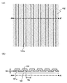
図16に、凹凸を有する下地膜上に形成された150nmの非晶質半導体膜に、凸部の長手方向に沿って、連続発振の出力エネルギー5.5Wのレーザー光を、走査速度が50cm/secとなるように照射したときの試料を、上面から観たTEMの像を示す。また、説明を分かり易くするために、図17に、図16に示したTEMの像を模式的に示す。 FIG. 16 shows that a 150 nm amorphous semiconductor film formed on a base film having irregularities is irradiated with laser light having a continuous oscillation output energy of 5.5 W along the longitudinal direction of the convex portion, with a scanning speed of 50 cm / cm. The TEM image which looked at the sample when irradiated so that it may become sec from the upper surface is shown. For easy understanding, FIG. 17 schematically shows the TEM image shown in FIG.
凸部8001の幅は0.5μm、凹部の幅は0.5μm、凸部の厚さは250nmである。図16、図17において、半導体膜のうち、8001に示す領域は凸部の上部に位置する部分に相当し、8002に示す領域は凹部の上部に位置する部分に相当する。なお凹部は、凸部が形成されていない窪んだ領域を指す。図17に示すとおり、凸部8001の上部において、半導体膜に粒界8003が形成されている。
The width of the
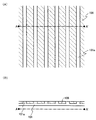
図18は、図16において示した試料と同じ条件で作製された試料を、セコエッチした後の、レーザー光の走査方向に対して垂直な方向における断面の、TEM像である。凹凸を有する下地膜は3層の絶縁膜から構成されており、窒化珪素からなる第1の絶縁膜上に、ストライプ状の酸化珪素からなる第2の絶縁膜を形成し、第1の絶縁膜と第2の絶縁膜を覆って酸化珪素からなる第3の絶縁膜が形成されている。 FIG. 18 is a TEM image of a cross section in a direction perpendicular to the scanning direction of the laser light after the sample manufactured under the same conditions as the sample shown in FIG. The base film having projections and depressions is composed of three layers of insulating films. A second insulating film made of stripe-shaped silicon oxide is formed on the first insulating film made of silicon nitride, and the first insulating film is formed. A third insulating film made of silicon oxide is formed so as to cover the second insulating film.
なおセコエッチは、K2Cr2O7とHFを混合した水溶液を用い、室温で75秒行なった。 Seco-etching was performed at room temperature for 75 seconds using an aqueous solution in which K 2 Cr 2 O 7 and HF were mixed.
図18に示すとおり、セコエッチにより凸部8009上の粒界8005が広がり、その位置がより明確になってる。なお、凸部8009内に見える白い部分は、セコエッチにより、半導体膜の粒界が広がり、該粒界を通して酸化珪素がエッチングされてしまっていることを示している。
As shown in FIG. 18, the
また図21は、図16、図18において示した試料と同じ条件で作製された試料を、セコエッチした後の、上面から見たTEM像である。セコエッチの条件は図18の場合と同じである。8501に示す領域は凸部の上部に位置する部分に相当し、8502に示す領域は凹部の上部に位置する部分に相当する。凸部8501の上部に位置する部分において見える白い部分は、セコエッチにより、半導体膜の粒界がエッチングされて広がっている部分を示しており、粒界が凸部8501の上部に選択的に形成されていることが明確になっている。
FIG. 21 is a TEM image viewed from the top after the sample manufactured under the same conditions as the samples shown in FIG. 16 and FIG. The conditions for the secco etch are the same as in FIG. A region indicated by 8501 corresponds to a portion located above the convex portion, and a region indicated by 8502 corresponds to a portion located above the concave portion. The white portion visible in the portion located above the
またレーザー光の照射により、図18において示した写真では、半導体膜8006の表面が平坦化されている。このことから本発明者らは、レーザー光の照射により一次的に半導体膜が溶融することで、絶縁膜の上部に位置していた半導体膜が凹部の底部方向に向かって体積移動し、そのため凸部の上に位置する半導体膜が薄くなり、応力に耐えられなくなったことが、凸部上に粒界が生じた要因の1つではないかと考えた。
In addition, the surface of the
また図19(A)〜図19(F)に、凹凸を有する絶縁膜上に形成された半導体膜にレーザー光を照射した際の、半導体膜における温度分布の経時変化のシミュレーション結果を示す。グラフで下側の凹凸が酸化膜で形成した下地膜8008を表している。また、上側のライン8009がシリコンと空気層の境界であり、レーザー光が照射されている部分を示している。酸化膜厚、シリコン膜厚ともに200nmで凹凸間隔は1μmとなっている。レーザー光照射の条件はガウシアンでピークエネルギー密度45000W/cm2で、σ=7×10-5secで設定した。
19A to 19F show simulation results of changes over time in the temperature distribution in the semiconductor film when the semiconductor film formed over the insulating film having unevenness is irradiated with laser light. In the graph, the unevenness on the lower side represents the
図19(A)がレーザー光の照射直後の温度分布を示しており、以下図19(B)〜図19(F)は、それぞれ2.5μsec後毎の温度分布を示している。 FIG. 19A shows the temperature distribution immediately after laser light irradiation, and FIGS. 19B to 19F show the temperature distribution after 2.5 μsec.
色が濃く示されている領域が、最も温度が高いと考えられる部分であり、図19(A)から図19(F)へ状態が移行するにつれて、色の濃い部分が少なくなっているのがわかる。特に、シリコン8009の温度は、時間の経過と共に、下地膜8008の凹部上の部分が、凸部上の部分よりも先に温度が低下しているのがわかる。
The region where the color is dark is the portion considered to have the highest temperature, and as the state transitions from FIG. 19A to FIG. 19F, the dark portion decreases. Recognize. In particular, it can be seen that the temperature of the
図20に、凹凸を有する絶縁膜上に形成された半導体膜にレーザー光を照射した際の、半導体膜の位置による温度の経時変化のシミュレーション結果を示す。 FIG. 20 shows a simulation result of a change in temperature over time depending on the position of the semiconductor film when the semiconductor film formed over the insulating film having unevenness is irradiated with laser light.
図20に示すグラフは、縦軸が半導体膜の温度(K)を示しており、横軸が時間(秒)を示している。実線は凸部上に位置する半導体膜の温度を示しており、破線が凹部上に位置する半導体膜の温度を示している。図20のシミュレーションでは、1600Kにおいて相転移にともない温度降下が一次停止しているが、相転移の後、破線で示した凹部上の半導体膜が、凸部上の半導体膜に比べて先に温度降下が開始されており、早く相転移しているのがわかる。 In the graph shown in FIG. 20, the vertical axis indicates the temperature (K) of the semiconductor film, and the horizontal axis indicates time (seconds). A solid line indicates the temperature of the semiconductor film located on the convex portion, and a broken line indicates the temperature of the semiconductor film located on the concave portion. In the simulation of FIG. 20, the temperature drop due to the phase transition stops at 1600 K, but after the phase transition, the temperature of the semiconductor film on the concave portion indicated by the broken line is higher than that of the semiconductor film on the convex portion. The descent has begun, and it can be seen that the phase transition is early.
これは、レーザー光の照射により半導体膜が溶融した後、該半導体膜内の熱が絶縁膜に放熱される際、絶縁膜と接している面積がより大きい部分において効率的に放熱が行われるためであると考えられる。よって、半導体膜と絶縁膜との接している面が平坦な部分よりも、接している面どうしが交わっている部分の方が絶縁膜への放熱が効率的である。また、絶縁膜の熱容量が大きい部分の方が、より効率的に放熱が行われる。例えば、凹部近傍の方が凸部近傍よりも、一定の範囲内における絶縁膜の体積が大きいため熱容量が大きいので、逃げた熱がこもりにくく、効率的に放熱が行われる。よって、凹部近傍の方が凸部近傍よりも結晶核が早く出来やすい。 This is because, after the semiconductor film is melted by laser light irradiation, when the heat in the semiconductor film is radiated to the insulating film, the heat is efficiently radiated in a portion where the area in contact with the insulating film is larger. It is thought that. Therefore, heat radiation to the insulating film is more efficient at the portion where the contacting surfaces intersect than the portion where the surface where the semiconductor film and the insulating film are in contact with each other is flat. In addition, heat is radiated more efficiently in the portion where the heat capacity of the insulating film is larger. For example, the heat capacity is larger in the vicinity of the concave portion than in the vicinity of the convex portion because the volume of the insulating film is larger within a certain range, so the escaped heat is less likely to be trapped and heat is efficiently dissipated. Therefore, crystal nuclei are more likely to be formed near the concave portion than at the convex portion.
そして時間の経過と共に、凹部近傍において生成された結晶核から、凸部上に向かって結晶成長が進む。そして隣り合う凹部近傍から進んだ結晶成長が、互いにその中間付近である凸部上においてぶつかり合うことが、凸部上に粒界が生じた要因の1つではないかと考えた。 As time elapses, crystal growth proceeds from the crystal nucleus generated in the vicinity of the concave portion toward the convex portion. Then, it was thought that the crystal growth proceeding from the vicinity of the adjacent concave portions collided with each other on the convex portions in the vicinity of each other may be one of the factors that caused the grain boundaries on the convex portions.
いずれにしろ、このように結晶化された半導体膜は、凸部の上部において粒界が選択的に形成される一方、凹部に位置する部分には粒界が形成されにくい。 In any case, in the crystallized semiconductor film, a grain boundary is selectively formed in the upper part of the convex part, whereas a grain boundary is hardly formed in a part located in the concave part.
そこで本発明者らは、レーザー光で結晶化された半導体膜のうち、凹部上に設けられた粒界の比較的少ない部分をTFTの活性層に用いることを考えた。 Therefore, the present inventors have considered using a portion of the semiconductor film crystallized by laser light with relatively few grain boundaries provided on the recess as the active layer of the TFT.
レーザー光は、連続発振であることが最も好ましいが、パルス発振のレーザー光を用いても良い。なおレーザー光の走査方向に対して垂直な方向における凸部の断面は、矩形を含む四角形が好ましく、または三角形であっても良い。 The laser light is most preferably continuous wave, but pulsed laser light may be used. Note that the cross section of the convex portion in the direction perpendicular to the scanning direction of the laser beam is preferably a quadrangle including a rectangle, or may be a triangle.
上記構成により、レーザー光の照射による結晶化の際、絶縁膜の凹部上に位置する半導体膜に、比較的粒界が形成されにくくすることができる。なお、絶縁膜の凹部上に位置する半導体膜は結晶性が優れているが、必ずしも粒界を含まないわけではない。しかし、たとえ粒界が存在したとしても絶縁膜の凸部上に位置する半導体膜に比較すると、その結晶粒は大きく、結晶性が比較的優れたものと言える。よって、絶縁膜の形状を設計した段階で、半導体膜の粒界の形成される位置をある程度予測することができる。つまり本発明では粒界が形成される位置を選択的に定めることができるので、活性層、より望ましくはチャネル形成領域に粒界がなるべく含まれないように、活性層をレイアウトすることが可能になる。 With the above structure, it is possible to make it relatively difficult to form a grain boundary in the semiconductor film located on the concave portion of the insulating film during crystallization by laser light irradiation. Note that the semiconductor film located on the concave portion of the insulating film has excellent crystallinity, but does not necessarily include a grain boundary. However, even if a grain boundary exists, it can be said that the crystal grains are large and the crystallinity is relatively excellent as compared with the semiconductor film positioned on the convex portion of the insulating film. Therefore, at the stage where the shape of the insulating film is designed, the position where the grain boundary of the semiconductor film is formed can be predicted to some extent. That is, according to the present invention, the position where the grain boundary is formed can be selectively determined, so that it is possible to lay out the active layer so that the grain boundary is not included in the active layer, more preferably the channel formation region. Become.
本発明では、絶縁膜の凹部上に位置する半導体膜を、TFTの活性層として積極的に用いることで、TFTのチャネル形成領域に粒界が形成されるのを防ぐことができ、粒界によってTFTの移動度が著しく低下したり、オン電流が低減したり、オフ電流が増加したりするのを防ぐことができる。なお、どこまでを凸部または凹部のエッジ近傍としてパターニングで除去するかは、設計者が適宜定めることができる。 In the present invention, the semiconductor film located on the recess of the insulating film is positively used as the active layer of the TFT, so that it is possible to prevent the formation of a grain boundary in the TFT channel formation region. It is possible to prevent the mobility of the TFT from being significantly lowered, the on-current is reduced, and the off-current is increased. It should be noted that the designer can appropriately determine how far is removed by patterning in the vicinity of the edge of the convex portion or the concave portion.
特に本発明では、半導体表示装置の画像を表示する画素部ではなく、画素部にビデオ信号やその他の信号を供給するための駆動回路において、上記構成を有するTFTを用いる。駆動回路は画素部に比べて、高い周波数で駆動させる必要があるため、本発明の上記構成のTFTを用いることは非常に有効である。また、活性層の結晶性が高められることで、活性層の大きさを抑えても所望の値のオン電流を得ることができるので、駆動回路全体の面積を抑えることができ、よって半導体表示装置全体に占める駆動回路の割合を抑えることができる。 In particular, in the present invention, the TFT having the above-described structure is used in a driving circuit for supplying a video signal and other signals to the pixel portion instead of the pixel portion for displaying an image of the semiconductor display device. Since the driving circuit needs to be driven at a higher frequency than the pixel portion, it is very effective to use the TFT having the above-described configuration of the present invention. Further, since the crystallinity of the active layer is enhanced, a desired value of on-current can be obtained even if the size of the active layer is suppressed, so that the area of the entire drive circuit can be suppressed, and thus the semiconductor display device The ratio of the drive circuit to the whole can be suppressed.
また本発明では、敢えて画素部において上記構成の凸部は設けずに、平坦な下地膜上に島状の半導体膜を形成する。画素部は、TFTの活性層や容量の電極として機能する島状の半導体膜のレイアウトによって、透過率が左右される。そのため、島状の半導体膜のレイアウトに関しては、駆動回路に比べて画素部の方が設計上の制約が大きく複雑であり、並列に配置された凸部間に島状の半導体膜をレイアウトするのが難しい。さらに画素部は駆動回路に比べて高速動作が要求されていないので、上記構成を有する島状の半導体膜を活性層とするTFTを用いなくとも、然程問題にはならず、かえって島状の半導体膜のレイアウトにおける設計上の制約が小さくなって望ましい。 In the present invention, an island-shaped semiconductor film is formed on a flat base film without providing the convex portion having the above structure in the pixel portion. The transmittance of the pixel portion depends on the layout of the island-shaped semiconductor film that functions as the active layer of the TFT and the electrode of the capacitor. Therefore, regarding the layout of the island-shaped semiconductor film, the pixel portion has a larger design restriction and is more complicated than the drive circuit, and the island-shaped semiconductor film is laid out between the convex portions arranged in parallel. Is difficult. Further, since the pixel portion is not required to operate at high speed as compared with the driver circuit, it does not matter so much without using the island-shaped semiconductor film having the above structure as an active layer. This is desirable because design constraints in the layout of the semiconductor film are reduced.
なお、レーザー光のレーザービームのエッジの近傍は、中央付近に比べて一般的にエネルギー密度が低く、半導体膜の結晶性も劣る場合が多い。そのためレーザー光を走査する際に、後にTFTのチャネル形成領域となる部分と、その軌跡のエッジとが重ならないようにするのが望ましい。また、最低限チャネル形成領域となる部分、より好ましくは凹部の平らな面全体に、一定のエネルギー密度のレーザー光を照射することが必要である。よって本発明では、レーザー光の走査により、均一なエネルギー密度を有する領域が、最低限チャネル形成領域となる部分、より好ましくは凹部の平らな面全体と完全に重なるような、エネルギー密度の分布を有するレーザービームを用いることが必要である。上記エネルギー密度の条件を満たすためには、レーザービームの形状を、矩形または線形等にすることが望ましいと考えられる。 Note that the energy density in the vicinity of the edge of the laser beam of the laser light is generally lower than that in the vicinity of the center, and the crystallinity of the semiconductor film is often poor. For this reason, when scanning with laser light, it is desirable that the portion that will later become the channel formation region of the TFT and the edge of the locus do not overlap. In addition, it is necessary to irradiate a laser beam having a certain energy density on a portion which becomes a channel forming region at least, more preferably on the entire flat surface of the recess. Therefore, in the present invention, the distribution of the energy density is such that the region having a uniform energy density is completely overlapped with the portion that becomes the channel formation region, more preferably the entire flat surface of the recess, by scanning with the laser beam. It is necessary to use a laser beam having. In order to satisfy the above energy density condition, it is desirable that the shape of the laser beam be rectangular or linear.
さらにスリットを介し、レーザービームのうちエネルギー密度の低い部分を遮蔽するようにしても良い。スリットを用いることで、比較的均一なエネルギー密度のレーザー光を凹部の平らな面全体または凸部の平らな面全体に照射することができ、結晶化を均一に行うことができる。またスリットを設けることで、絶縁膜または半導体膜のパターン情報によって部分的にレーザービームの幅を変えることができ、チャネル形成領域、さらにはTFTの活性層のレイアウトにおける制約を小さくすることができる。なおレーザービームの幅とは、走査方向と垂直な方向におけるレーザービームの長さを意味する。 Further, a portion of the laser beam having a low energy density may be shielded through a slit. By using the slit, a laser beam having a relatively uniform energy density can be applied to the entire flat surface of the concave portion or the entire flat surface of the convex portion, and crystallization can be performed uniformly. Further, by providing the slit, the width of the laser beam can be partially changed depending on the pattern information of the insulating film or the semiconductor film, and the restrictions on the layout of the channel formation region and the active layer of the TFT can be reduced. The width of the laser beam means the length of the laser beam in the direction perpendicular to the scanning direction.
また複数のレーザー発振装置から発振されたレーザー光を合成することで得られた1つのレーザービームを、レーザー結晶化に用いても良い。上記構成により、各レーザー光のエネルギー密度の弱い部分を補い合うことができる。 A single laser beam obtained by synthesizing laser beams oscillated from a plurality of laser oscillation devices may be used for laser crystallization. With the above configuration, it is possible to compensate for the weak energy density of each laser beam.
また半導体膜を成膜した後、大気に曝さないように(例えば希ガス、窒素、酸素等の特定されたガス雰囲気または減圧雰囲気にする)レーザー光の照射を行い、半導体膜を結晶化させても良い。上記構成により、クリーンルーム内における分子レベルでの汚染物質、例えば空気の清浄度を高めるためのフィルター内に含まれるボロン等が、レーザー光による結晶化の際に半導体膜に混入するのを防ぐことができる。 In addition, after the semiconductor film is formed, laser light irradiation is performed so that the semiconductor film is not crystallized so that the semiconductor film is not exposed to the air (for example, a specified gas atmosphere such as a rare gas, nitrogen, oxygen, or a reduced pressure atmosphere). Also good. With the above configuration, contaminants at the molecular level in the clean room, such as boron contained in a filter for increasing the cleanliness of air, can be prevented from being mixed into the semiconductor film during crystallization by laser light. it can.
本発明では、下地膜の凹部上に位置する島状の半導体膜を、TFTの活性層として積極的に用いることで、TFTのチャネル形成領域に粒界が形成されるのを防ぐことができ、粒界によってTFTの移動度が著しく低下したり、オン電流が低減したり、オフ電流が増加したりするのを防ぐことができる。なお、どこまでを凸部または凹部のエッジ近傍としてパターニングで除去するかは、設計者が適宜定めることができる。 In the present invention, it is possible to prevent the formation of grain boundaries in the channel formation region of the TFT by actively using the island-shaped semiconductor film located on the recess of the base film as the active layer of the TFT. It is possible to prevent the mobility of the TFT from being significantly lowered by the grain boundary, the on-current is reduced, and the off-current is increased. It should be noted that the designer can appropriately determine how far is removed by patterning in the vicinity of the edge of the convex portion or the concave portion.
特に本発明では、半導体表示装置の画像を表示する画素部ではなく、画素部にビデオ信号やその他の信号を供給するための駆動回路において、上記構成を有するTFTを用いる。駆動回路は画素部に比べて、高い周波数で駆動させる必要があるため、本発明の上記構成のTFTを用いることは非常に有効である。また、活性層の結晶性が高められることで、活性層の大きさを抑えても所望の値のオン電流を得ることができるので、駆動回路全体の面積を抑えることができ、よって半導体表示装置全体に占める駆動回路の割合を抑えることができる。 In particular, in the present invention, the TFT having the above-described structure is used in a driving circuit for supplying a video signal and other signals to the pixel portion instead of the pixel portion for displaying an image of the semiconductor display device. Since the driving circuit needs to be driven at a higher frequency than the pixel portion, it is very effective to use the TFT having the above-described configuration of the present invention. Further, since the crystallinity of the active layer is enhanced, a desired value of on-current can be obtained even if the size of the active layer is suppressed, so that the area of the entire drive circuit can be suppressed, and thus the semiconductor display device The ratio of the drive circuit to the whole can be suppressed.
また本発明では、敢えて画素部において上記構成の凸部は設けずに、平坦な下地膜上に島状の半導体膜を形成する。画素部は、TFTの活性層や容量の電極として機能する島状の半導体膜のレイアウトによって、透過率が左右される。そのため、島状の半導体膜のレイアウトに関しては、駆動回路に比べて画素部の方が設計上の制約が大きく複雑であり、並列された凸部間に島状の半導体膜をレイアウトするのが難しい。さらに画素部は駆動回路に比べて高速動作が要求されていないので、上記構成を有する島状の半導体膜を活性層とするTFTを用いなくとも、然程問題にはならず、かえって島状の半導体膜のレイアウトにおける設計上の制約が小さくなって望ましい。 In the present invention, an island-shaped semiconductor film is formed on a flat base film without providing the convex portion having the above structure in the pixel portion. The transmittance of the pixel portion depends on the layout of the island-shaped semiconductor film that functions as the active layer of the TFT and the electrode of the capacitor. For this reason, regarding the layout of the island-shaped semiconductor film, the pixel portion has more design restrictions and is more complicated than the drive circuit, and it is difficult to lay out the island-shaped semiconductor film between the convex portions arranged in parallel. . Further, since the pixel portion is not required to operate at high speed as compared with the driver circuit, it does not matter so much without using the island-shaped semiconductor film having the above structure as an active layer. This is desirable because design constraints in the layout of the semiconductor film are reduced.
次に、本発明の半導体表示装置の作製方法について説明する。 Next, a method for manufacturing a semiconductor display device of the present invention will be described.
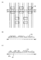
まず、図1(A)に示すように、矩形またはストライプ形状の凸部101aを有する下地膜101を基板上に形成する。図1(A)のA−A’における断面図が図1(B)に相当する。
First, as shown in FIG. 1A, a
基板(図示せず)は、後の工程の処理温度に耐えうる材質であれば良く、例えば石英基板、シリコン基板、バリウムホウケイ酸ガラスまたはアルミノホウケイ酸ガラスなどのガラス基板、金属基板またはステンレス基板の表面に絶縁膜を形成した基板を用いることができる。また、処理温度に耐えうる程度に耐熱性を有するプラスチック基板を用いてもよい。 The substrate (not shown) may be any material that can withstand the processing temperature of the subsequent process. For example, a quartz substrate, a silicon substrate, a glass substrate such as barium borosilicate glass or aluminoborosilicate glass, a metal substrate, or a stainless substrate. A substrate having an insulating film formed on the surface can be used. Further, a plastic substrate having heat resistance enough to withstand the processing temperature may be used.
また本実施の形態では、下地膜101として酸化珪素膜を用いた。なお、下地膜101の材料はこれに限定されず、後の工程における熱処理に耐え得る材料で、なおかつTFTの特性に悪影響を与えうるアルカリ金属が、後に形成される半導体膜に混入するのを防ぐことができ、凹凸を形成することができる絶縁膜であれば良い。なおこの凹凸の形成の仕方については、後段において詳しく説明する。また、これらの他の絶縁膜を用いても良いし、単一の層からなる絶縁膜ではなく2層以上の絶縁膜の積層構造であってもよい。
In this embodiment mode, a silicon oxide film is used as the
次に、下地膜101を覆うように、半導体膜102を形成する。半導体膜102は、公知の手段(スパッタ法、LPCVD法、プラズマCVD法等)により成膜することができる。なお、半導体膜は非晶質半導体膜であっても良いし、微結晶半導体膜、結晶質半導体膜であっても良い。また珪素だけではなくシリコンゲルマニウムを用いるようにしても良い。シリコンゲルマニウムを用いる場合、ゲルマニウムの濃度は0.01〜4.5atomic%程度であることが好ましい。また、下地膜101を成膜した後、大気開放せずに連続的に成膜することで、半導体膜と下地膜との間に不純物が混入するのを防ぐことができる。
Next, the
なお、凸部間の幅が大きすぎたり小さすぎたりすると、本発明の効果は得られない。また凸部の高さが高すぎると、後に形成される半導体膜が凸部のエッジ近傍において膜切れを起こす可能性が高くなる。また、低すぎても本発明の効果は得られない。凸部101aの断面形状及びそのサイズついては、半導体膜の厚さとの兼ね合いを考慮し、設計者が適宜設定することができる。凸部間の幅Wsは0.01μm〜2μm、より望ましくは0.1μm〜1μm程度にするのが好ましい。また、凸部の高さWhは0.01μm〜3μm、より望ましくは0.1μm〜2μm程度にするのが好ましい。または凸部の高さを小さくし、Whを0.01μm〜1μm、より望ましくは0.05μm〜0.2μm程度にしても良い。
In addition, the effect of this invention will not be acquired if the width | variety between convex parts is too large or too small. Further, if the height of the convex portion is too high, there is a high possibility that a semiconductor film to be formed later will be cut near the edge of the convex portion. Moreover, even if it is too low, the effect of the present invention cannot be obtained. The cross-sectional shape and size of the
次に、図2(A)に示すように、半導体膜102にレーザー光を照射する。なお、図2(B)は、図2(A)の破線A−A’における断面図に相当する。
Next, as shown in FIG. 2A, the
本実施の形態では、図2(A)において矢印で示したように、走査方向を矩形の凸部101aの長手方向に揃えてレーザー光を照射したが、本発明はこの構成に限定されない。レーザー光の走査方向は設計者が適宜設定することが可能である。レーザー光の照射により、半導体膜102は一次的に溶融し、図2(B)において白抜きの矢印で示したように、凸部の上部から凹部に向かってその体積が移動する。そして表面が平坦化され、なおかつ結晶性が高められた半導体膜103が形成される。レーザー光のエネルギー密度は、レーザービームのエッジの近傍において低くなっており、そのためエッジの近傍は結晶粒が小さく、結晶の粒界に沿って突起した部分(リッジ)が出現する。そのため、レーザー光のレーザービームの軌跡のエッジと、チャネル形成領域となる部分または半導体膜102の凹部上に位置する部分とが重ならないように照射する。
In this embodiment mode, as shown by arrows in FIG. 2A, the laser beam is irradiated with the scanning direction aligned with the longitudinal direction of the rectangular
本発明では公知のレーザーを用いることができる。レーザー光は連続発振であることが望ましいが、パルス発振であってもある程度本発明の効果を得ることができると考えられる。レーザーは、気体レーザーもしくは固体レーザーを用いることができる。気体レーザーとして、エキシマレーザー、Arレーザー、Krレーザーなどがあり、固体レーザーとして、YAGレーザー、YVO4レーザー、YLFレーザー、YAlO3レーザー、ガラスレーザー、ルビーレーザー、アレキサンドライドレーザー、Ti:サファイアレーザーなどが挙げられる。固体レーザーとしては、Cr、Nd、Er、Ho、Ce、Co、Ti又はTmがドーピングされたYAG、YVO4、YLF、YAlO3などの結晶を使ったレーザーが適用される。当該レーザーの基本波はドーピングする材料によって異なり、1μm前後の基本波を有するレーザー光が得られる。基本波に対する高調波は、非線形光学素子を用いることで得ることができる。 In the present invention, a known laser can be used. Although it is desirable that the laser light is continuous oscillation, it is considered that the effect of the present invention can be obtained to some extent even if it is pulse oscillation. As the laser, a gas laser or a solid laser can be used. Examples of gas lasers include excimer laser, Ar laser, and Kr laser. Examples of solid-state lasers include YAG laser, YVO 4 laser, YLF laser, YAlO 3 laser, glass laser, ruby laser, alexandride laser, and Ti: sapphire laser. Can be mentioned. As the solid-state laser, a laser using a crystal such as YAG, YVO 4 , YLF, YAlO 3 doped with Cr, Nd, Er, Ho, Ce, Co, Ti, or Tm is applied. The fundamental wave of the laser differs depending on the material to be doped, and a laser beam having a fundamental wave of about 1 μm can be obtained. The harmonic with respect to the fundamental wave can be obtained by using a nonlinear optical element.
またさらに、固体レーザーから発せられらた赤外レーザー光を非線形光学素子でグリーンレーザー光に変換後、さらに別の非線形光学素子によって得られる紫外レーザー光を用いることもできる。 Furthermore, after converting infrared laser light emitted from a solid-state laser into green laser light using a nonlinear optical element, ultraviolet laser light obtained by another nonlinear optical element can also be used.
半導体膜103は、レーザー光の照射による体積移動により、下地膜101の凹部上において膜厚が厚くなり、逆に凸部101a上において膜厚が薄くなっている。そのため応力によって凸部上に粒界104が発生しやすく、逆に凹部上においては結晶性の良い状態が得られる。なお、凹部上において半導体膜103が必ずしも粒界を含まないわけではない。しかし、たとえ粒界が存在したとしても結晶粒が大きいので、結晶性は比較的優れたものとなっている。
The
なお、半導体膜の結晶化に際し、レーザー光の照射の工程と、触媒を用いて半導体膜を結晶化させる工程とを組み合わせていても良い。触媒元素を用いる場合、特開平7−130652号公報、特開平8−78329号公報で開示された技術を用いることができる。 Note that in crystallization of the semiconductor film, a laser light irradiation process may be combined with a process of crystallizing the semiconductor film using a catalyst. In the case of using a catalyst element, the techniques disclosed in Japanese Patent Application Laid-Open Nos. 7-130652 and 8-78329 can be used.
次に、図3(A)に示すように、半導体膜103の表面をエッチングしていき、下地膜101の凸部101aの上面を露出させる。なお、図3(B)は、図3(A)の破線A−A’における断面図に相当する。上記工程により、下地膜101の凹部に存在する半導体膜105が形成される。半導体膜103の上面からの除去は、どのような方法を用いて行っても良く、例えばエッチングにより行っても良いし、CMP法により行っても良い。
Next, as shown in FIG. 3A, the surface of the
この上面からの除去により、凸部101a上の粒界が存在する部分が除去され、凸部101a間に相当する凹部の上には、後にチャネル形成領域となる結晶性の良い半導体膜が残される。
By removing from the upper surface, a portion where the grain boundary exists on the
次に、図4(A)に示すように半導体膜105をパターニングすることで、活性層となる島状の半導体膜106を形成する。なお、図4(B)は、図4(A)
の破線A−A’における断面図に相当する。島状の半導体膜106は、凸部101a間に形成される凹部上にその一部が存在する。さらに、半導体膜106は、その一部が凸部101aと接している。TFTのチャネル形成領域は、半導体膜105の凹部上に位置する部分を用いて形成されるように、そのチャネル長、チャネル幅を考慮して、凸部101aのレイアウトを定めるのが望ましい。なお、ソース領域またはドレイン領域となる部分をも凹部上に存在する半導体膜で形成することで、ソース領域とドレイン領域の抵抗を下げることができる。
Next, as shown in FIG. 4A, the
Corresponds to a cross-sectional view taken along a broken line AA ′. A part of the island-shaped
なお、図4では各島状の半導体膜106が、凸部101aと重なっていないが、本発明はこの構成に限定されない。島状の半導体膜106の一部が凸部101a上に重なっていても良い。さらに、互いに分離した複数のチャネル形成領域と、全ての複数のチャネル形成領域を間に挟んでいるソース領域及びドレイン領域とを有し、全ての複数のチャネル形成領域が凸部101aと重なっておらず、ソース領域及びドレイン領域は凸部と一部重なっている、所謂マルチチャネル型のTFTであっても良い。
In FIG. 4, each island-shaped
また、図4では凸部101aが残ったままであるが、島状の半導体膜106を形成した後、凸部101aを除去しても良い。図12(A)に凸部101aを除去した後の島状の半導体膜106の様子を示す。また図12(A)のA−A’における断面図を図12(B)に示す。
Further, although the
上述した一連の工程によって得られた島状の半導体膜を活性層として用い、TFTを作製する。互いに分離した複数のチャネル形成領域を有するTFTの作製工程及びその具体的な構造は様々である。代表的には、島状の半導体膜に不純物を添加し、ソース領域とドレイン領域を形成する工程と、ゲート絶縁膜を形成する工程と、ゲート電極を形成する工程とが行われる。 A TFT is manufactured using the island-shaped semiconductor film obtained by the series of steps described above as an active layer. There are various manufacturing processes and specific structures of TFTs having a plurality of channel formation regions separated from each other. Typically, an impurity is added to the island-shaped semiconductor film to form a source region and a drain region, a step of forming a gate insulating film, and a step of forming a gate electrode.
なお、本実施の形態ではレーザー光で結晶化した半導体膜の表面を、凸部が露出する程度に除去する工程の後に、パターニングにより島状の半導体膜を形成する工程を行なっているが、本発明はこの構成に限定されない。パターニングにより島状の半導体膜を形成する工程の後に、凸部が露出する程度に島状の半導体膜の表面を除去する工程を行なっても良い。また、半導体膜をパターニングしてからレーザーで結晶化するようにしても良い。 Note that in this embodiment, after the step of removing the surface of the semiconductor film crystallized with laser light to the extent that the protrusions are exposed, a step of forming an island-shaped semiconductor film by patterning is performed. The invention is not limited to this configuration. After the step of forming the island-shaped semiconductor film by patterning, a step of removing the surface of the island-shaped semiconductor film to such an extent that the protrusions are exposed may be performed. Alternatively, the semiconductor film may be patterned and then crystallized with a laser.
本発明では、絶縁膜の凹部上に位置する半導体膜を、TFTの活性層として積極的に用いることで、TFTのチャネル形成領域に粒界が形成されるのを防ぐことができ、粒界によってTFTの移動度が著しく低下したり、オン電流が低減したり、オフ電流が増加したりするのを防ぐことができ、TFTの特性のバラツキを抑えることができる。 In the present invention, the semiconductor film located on the recess of the insulating film is positively used as the active layer of the TFT, so that it is possible to prevent the formation of a grain boundary in the TFT channel formation region. The mobility of the TFT can be remarkably lowered, the on-current can be prevented from decreasing, and the off-current can be prevented from increasing, and variations in TFT characteristics can be suppressed.
そして、TFTを作製した後、目的とする回路の仕様に合わせて、各TFTのゲート電極、ソース領域、ドレイン領域を電気的に接続する配線を形成する。図5に、上記TFTを用いてインバーターとトランスミッションゲートを作製した例について説明する。 Then, after the TFT is manufactured, a wiring for electrically connecting the gate electrode, the source region, and the drain region of each TFT is formed in accordance with the specification of the target circuit. FIG. 5 illustrates an example in which an inverter and a transmission gate are manufactured using the TFT.
図5(A)に、本発明の作製方法を用いて形成されたインバーターとトランスミッションゲートの上面図を、図5(B)にその回路図を示す。上述した一連の作製方法を用いて形成された島状の半導体膜を用いて、pチャネル型TFT110、111、nチャネル型TFT112、113を形成する。これらのTFT110〜113は、少なくとも活性層と、ゲート絶縁膜と、ゲート電極とをそれぞれ有している。そして各活性層にはチャネル形成領域と、該チャネル形成領域を挟んでいるソース領域とドレイン領域とが少なくとも設けられている。
FIG. 5A shows a top view of an inverter and a transmission gate formed by using the manufacturing method of the present invention, and FIG. 5B shows a circuit diagram thereof. The p-
なお、ソース領域またはドレイン領域となる不純物領域と、チャネル形成領域との間にLDD領域やオフセット領域を有していてもよい。 Note that an LDD region or an offset region may be provided between an impurity region serving as a source region or a drain region and a channel formation region.
各TFTは凹部上に活性層を有しており、各活性層は凸部101a間に位置し、かつ凸部101aとは重なっていない。そして、配線115〜120によって、各TFTのソース領域、ドレイン領域またはゲート電極が接続されることで、図5(B)に示した回路図を有する回路を形成することができる。具体的には、pチャネル型TFT110とnチャネル型TFT112とでインバーターが形成されている。また、pチャネル型TFT111とnチャネル型TFT113とでトランスミッションゲートが形成されている。Aに入力された信号に同期して、Inから入力された信号がサンプリングされOutから出力される。
Each TFT has an active layer on the concave portion, and each active layer is located between the
上記構成により、回路の仕様を変更するときに、予め用意されているTFTまたは論理素子を接続する配線のレイアウトのみ変更すれば良い。例えば図5の場合では、配線のパターニング用のマスクと、配線のコンタクトホール用のマスクの少なくとも2枚変更すれば良い。よって、回路の設計変更に伴うコストを抑えることができ、なおかつ様々な仕様の回路を作製することができる。 With the above configuration, when the circuit specifications are changed, only the wiring layout for connecting TFTs or logic elements prepared in advance needs to be changed. For example, in the case of FIG. 5, it is sufficient to change at least two masks, ie, a wiring pattern mask and a wiring contact hole mask. Therefore, costs associated with circuit design changes can be suppressed, and circuits with various specifications can be manufactured.
なお、本発明は上記回路に限定されないことは言うまでもない。また、図5(A)では、配線115〜120が同じ層に形成されているが、本発明はこれに限定されない。各TFTを接続する配線は、異なる層に形成されていても良い。各配線を異なる層に形成することで、複雑な接続が可能になり、同じ数のTFTから形成することができる回路の種類が豊富になる。なおTFTの接続は、ダマシンプロセス等によって作製された配線(プラグ)によって行なっても良い。
Needless to say, the present invention is not limited to the above circuit. In FIG. 5A, the
なお、上記工程において、レーザー光の照射後または結晶化後の半導体膜を下地膜の凸部が露出する程度にエッチングした後において、500〜600℃で1分から60分程度加熱することで、半導体膜内において生じている応力を緩和することができる。 In the above process, after etching the semiconductor film after laser light irradiation or crystallization to such an extent that the convex portions of the base film are exposed, the semiconductor film is heated at 500 to 600 ° C. for about 1 to 60 minutes. The stress generated in the film can be relaxed.
本発明の作製方法で、例えばLSIを用いたCPU、各種ロジック回路の記憶素子(例えばSRAM)、カウンタ回路、分周回路ロジック等を形成することができる。本発明は、様々な半導体表示装置に適用させることが可能である。 With the manufacturing method of the present invention, for example, a CPU using an LSI, a memory element (eg, SRAM) of various logic circuits, a counter circuit, a divider circuit logic, or the like can be formed. The present invention can be applied to various semiconductor display devices.
次に、上記構成を有する本発明の半導体表示装置の構成について説明する。図6(A)に一般的な半導体表示装置の、基板の上面図を示す。図6(A)では、基板4001上に、後に画素部4002と、画素部にビデオ信号やその他の信号または電源を供給するための駆動回路4003、4004を有している。なお図6(A)では島状の半導体膜が形成された時点での様子を示している。
Next, the structure of the semiconductor display device of the present invention having the above structure will be described. FIG. 6A shows a top view of a substrate of a general semiconductor display device. 6A, a
駆動回路4004は走査線駆動回路であり、画素部4002に複数形成される画素を順に選択するための回路である。駆動回路4003は信号線駆動回路であり、走査線駆動回路4004によって選択された画素に、所定のタイミングでビデオ信号を入力するための回路である。なお図6(A)では、半導体表示装置の基板の、代表的な構成を示したものであり、本発明の半導体表示装置はこの構成に限定されない。
A
そして本発明では、駆動回路4003、4004において、図1に示したような、凸部を有する絶縁膜上においてレーザー光で結晶化された島状の半導体膜が形成されている。一方画素部4002において形成される島状の半導体膜は、平坦な絶縁膜上に形成されている。
In the present invention, in the driving
図6(B)に、図6(A)の信号線駆動回路4003の一部と画素部4002を含む領域4005の拡大図を示す。信号線駆動回路4003は、ストライプ状または矩形状の複数の凸部4006を有しており、該凸部4006間に島状の半導体膜4007を有している。島状の半導体膜4007は図1に示した作製方法を用いて形成されている。
FIG. 6B is an enlarged view of a
図示してはいないが、走査線駆動回路4004においても同様に、ストライプ状または矩形状の複数の凸部が形成され、該凸部間に島状の半導体膜が形成されていても良い。ただし、基板上に形成される全ての凸部の長手方向を揃えた方が、TFTの特性のバラツキを抑えるためには、より望ましい。
Although not shown, in the scan
駆動回路は画素部に比べて、高い周波数で駆動させる必要があるため、本発明の上記構成の島状の半導体膜を活性層としたTFTを用いることは非常に有効である。また、活性層の結晶性が高められることで、活性層の大きさを抑えても所望の値のオン電流を得ることができるので、駆動回路全体の面積を抑えることができ、よって半導体表示装置全体に占める駆動回路の割合を抑えることができる。 Since the driving circuit needs to be driven at a higher frequency than the pixel portion, it is very effective to use a TFT having an island-shaped semiconductor film having the above-described structure according to the present invention as an active layer. Further, since the crystallinity of the active layer is enhanced, a desired value of on-current can be obtained even if the size of the active layer is suppressed, so that the area of the entire drive circuit can be suppressed, and thus the semiconductor display device The ratio of the drive circuit to the whole can be suppressed.
また本発明では、敢えて画素部において上記構成の凸部は設けずに、平坦な下地膜上に島状の半導体膜を形成する。画素部は、TFTの活性層や容量の電極として機能する島状の半導体膜のレイアウトによって、透過率が左右される。そのため、島状の半導体膜のレイアウトに関しては、駆動回路に比べて画素部の方が設計上の制約が大きく複雑であり、並列された凸部間に島状の半導体膜をレイアウトするのが難しい。さらに画素部は駆動回路に比べて高速動作が要求されていないので、上記構成を有する島状の半導体膜を活性層とするTFTを用いなくとも、然程問題にはならず、かえって島状の半導体膜のレイアウトにおける設計上の制約が小さくなって望ましい。 In the present invention, an island-shaped semiconductor film is formed on a flat base film without providing the convex portion having the above structure in the pixel portion. The transmittance of the pixel portion depends on the layout of the island-shaped semiconductor film that functions as the active layer of the TFT and the electrode of the capacitor. For this reason, regarding the layout of the island-shaped semiconductor film, the pixel portion has more design restrictions and is more complicated than the drive circuit, and it is difficult to lay out the island-shaped semiconductor film between the convex portions arranged in parallel. . Further, since the pixel portion is not required to operate at high speed as compared with the driver circuit, it does not matter so much without using the island-shaped semiconductor film having the above structure as an active layer. This is desirable because design constraints in the layout of the semiconductor film are reduced.
なお本実施の形態では、島状の半導体膜が凸部間にのみ存在している例を示したが、本発明はこの構成に限定されない。島状の半導体膜の一部が、凸部上に重なって形成されていても良いし、島状の半導体膜が部分的に凸部と接していてもいなくても良い。また、島状の半導体膜を形成した後、下地膜の凸部のみを除去するようにしても良い。 Note that although an example in which the island-shaped semiconductor film exists only between the protrusions is described in this embodiment mode, the present invention is not limited to this structure. A part of the island-shaped semiconductor film may be formed so as to overlap the convex portion, or the island-shaped semiconductor film may or may not partially touch the convex portion. In addition, after the island-shaped semiconductor film is formed, only the convex portion of the base film may be removed.
また、電熱炉を使用した熱結晶化方法、赤外光を用いたランプアニール結晶化法を用いて、駆動回路及び画素部に形成された半導体膜を結晶化した後、駆動回路においてのみレーザー光を用いてより結晶性が高められるように結晶化させても良い。 In addition, after crystallizing the semiconductor film formed in the driver circuit and the pixel portion using a thermal crystallization method using an electric furnace and a lamp annealing crystallization method using infrared light, laser light is emitted only in the driver circuit. May be used for crystallization so that the crystallinity is further improved.
または、駆動回路及び画素部に形成された半導体膜に、膜厚方向において完全に溶解しないような低いエネルギーのレーザー光を照射して結晶化した後、駆動回路においてのみ膜厚方向において完全に溶解するような高いエネルギーのレーザー光を照射するようにしても良い。あるいは、駆動回路及においてのみ、形成された半導体膜に、膜厚方向において完全に溶解しないような低いエネルギーのレーザー光を照射して結晶化した後、膜厚方向において完全に溶解するような高いエネルギーのレーザー光を照射するようにしても良い。 Alternatively, the semiconductor film formed in the driver circuit and the pixel portion is crystallized by irradiating with low energy laser light that does not completely dissolve in the film thickness direction, and then completely dissolved in the film thickness direction only in the driver circuit. Such high energy laser light may be irradiated. Alternatively, only in the driving circuit and the semiconductor film, the formed semiconductor film is irradiated with a low energy laser beam that does not completely dissolve in the film thickness direction, and is crystallized. You may make it irradiate the laser beam of energy.
以下、本発明の実施例について説明する。 Examples of the present invention will be described below.
本実施例では、実施の形態において島状の半導体膜を形成した後に、凸部を一部除去する例について説明する。 In this example, an example in which part of the protrusion is removed after the island-shaped semiconductor film is formed in the embodiment will be described.
まず、実施の形態の図2に示した状態まで作製する。そして、図7(A)に示すように、後の工程においてTFTのチャネル形成領域となる部分のみを残してマスク170で覆う。そして、この状態で半導体膜103の表面をエッチングしていき、下地膜101の凸部101aの上面を露出させる。なお、図7(B)は、図7(A)の破線B−B’における断面図に相当する。また、図7(C)は、図7(A)の破線C−C’における断面図に相当する。上記工程により、下地膜101の凹部に存在する半導体膜171が形成される。半導体膜103の上面からの除去は、どのような方法を用いて行っても良いが、本実施例ではエッチングで除去した。
First, the state shown in FIG. 2 of the embodiment is manufactured. Then, as shown in FIG. 7A, in a later step, only a portion that becomes a channel formation region of the TFT is left and covered with a
この上面からの除去により、マスクで覆われていない部分において、凸部101a上の粒界が存在する部分が除去される。凸部101a間に相当する凹部の上には、後にチャネル形成領域となる結晶性の良い半導体膜が残される。
By the removal from the upper surface, a portion where the grain boundary on the
そして、図7に示した状態まで作製した後、半導体膜171をパターニングし、図8(A)に示すように島状の半導体膜172を形成した。図8(B)は図8(A)のB−B’における断面図に相当する。また、図8(C)は、図8(A)
の破線C−C’における断面図に相当する。島状の半導体膜172は、チャネル形成領域となる部分と、ソース領域又はドレイン領域となる部分とで、厚さに差が生じている。またソース領域またはドレイン領域となる部分は、その一部が凸部101a上に重なっていても良い。
Then, after producing the state shown in FIG. 7, the
Corresponds to a cross-sectional view taken along the broken line CC ′. The island-shaped
本実施例のようにソース領域とドレイン領域の一部が凸部101aと重なっていることで、ソース領域とドレイン領域の表面を広く確保することができるので、ソース領域またはドレイン領域に接続される配線のコンタクトホールのレイアウトのマージンを大きくとることができる。
Since a part of the source region and the drain region overlaps with the
また、平坦な下地膜上の半導体膜の上に形成された絶縁膜にコンタクトホールを形成する際に、コンタクトホールのマスクがずれると、半導体膜の下に位置する下地膜がエッチングされて、該半導体膜に接するように形成された電極が断切れを起こすことがある。本発明では半導体膜の、特にソース領域とドレイン領域となる部分が、凸部と接するようにすることで、半導体膜の下に位置する下地膜の代わりに、凸部の一部がエッチングされるので、ソース領域またはドレイン領域に接する配線の断切れを防ぐことができる。 In addition, when forming a contact hole in an insulating film formed over a semiconductor film on a flat base film, if the mask of the contact hole is shifted, the base film located under the semiconductor film is etched, An electrode formed so as to be in contact with the semiconductor film may break off. In the present invention, a part of the convex portion is etched instead of the base film located under the semiconductor film by making the portions of the semiconductor film, especially the source region and the drain region, contact the convex portion. Therefore, disconnection of the wiring in contact with the source region or the drain region can be prevented.
本実施例では、可撓性を有する基板を用いた本発明の半導体表示装置について説明する。可撓性を有する基板を用いた半導体表示装置は、厚みが薄く軽量であるということに加えて、曲面を有するディスプレイや、ショーウィンドウ等などにも用いることができる。よって、その用途は携帯機器のみに限られず、応用範囲は多岐にわたる。 In this embodiment, a semiconductor display device of the present invention using a flexible substrate will be described. A semiconductor display device using a flexible substrate can be used for a display with a curved surface, a show window, and the like in addition to being thin and lightweight. Therefore, the application is not limited to portable devices, and the range of applications is diverse.
基板が非平面の場合、課題となるのは、曲率をどこまで高められるかということである。基板の曲率を高めていくと、基板上に成膜された絶縁膜に生じる応力によって、該絶縁膜上に形成される半導体素子が、所望の特性を得られなくなるという事態が生じる。特に絶縁膜の厚さが増してくるとその傾向が強い。 When the substrate is non-planar, the problem is how much the curvature can be increased. When the curvature of the substrate is increased, a situation occurs in which the semiconductor element formed on the insulating film cannot obtain desired characteristics due to the stress generated in the insulating film formed on the substrate. This tendency is particularly strong as the thickness of the insulating film increases.
そこで本実施例では、絶縁膜で形成された下地膜が有する凸部の長手方向と、基板の母線方向とを同じ向きに保つようにする。図9に、可撓性を有する基板を用いて形成された半導体表示装置を、湾曲させた様子を示す。基板5001には、画素部5002、走査線駆動回路5003及び信号線駆動回路5004が形成されている。基板5001には、後の工程における処理温度に耐え得る素材を用いる。
Therefore, in this embodiment, the longitudinal direction of the convex portion of the base film formed of the insulating film is kept in the same direction as the busbar direction of the substrate. FIG. 9 shows a curved shape of a semiconductor display device formed using a flexible substrate. A
走査線駆動回路5003及び信号線駆動回路5004において、凸部を有する下地膜5005上に形成された島状の半導体膜を用いてTFTが形成されている。そして、下地膜5005の凸部の長手方向と、基板5001の母線の方向とが実線の矢印で示すように共に一致している。このように下地膜の凸部の長手方向と、基板の母線の方向とを一致させることで、下地膜に生じる応力を分散させることができる。
In the scan
本実施例は、実施例1と自由に組み合わせて実施することが可能である。 This embodiment can be implemented by freely combining with the first embodiment.
本実施例では、半導体膜の結晶化に際し、レーザー光の照射の工程と、触媒を用いて半導体膜を結晶化させる工程とを組み合わせた例について説明する。触媒元素を用いる場合、例えば特開平6−349735号公報で開示された技術を用いることができる。 In this embodiment, an example in which a laser light irradiation process and a semiconductor film crystallization process using a catalyst are combined in crystallization of a semiconductor film will be described. In the case of using a catalyst element, for example, the technique disclosed in JP-A-6-349735 can be used.
まず、図10(A)に示すように、基板上に絶縁膜からなる第1下地膜350を成膜する。第1下地膜350は本実施例では酸化窒化珪素を用いるがこれに限定されず、後に形成される第2下地膜351とエッチングにおける選択比が大きい絶縁膜であれば良い。本実施例では第1下地膜350をCVD装置でSiH4とN2Oを用いて50〜200nmの厚さになるように形成した。なお第1下地膜は単層であっても、複数の絶縁膜を積層した構造であってもよい。
First, as shown in FIG. 10A, a
次に第1下地膜350に接するように、絶縁膜からなる第2下地膜351を形成する。本実施例では第2下地膜351として、プラズマCVD法を用いて30nm〜300nmの酸化珪素を形成する。
Next, a
次に、図10(B)に示すように、マスク352を形成し、第2下地膜351をエッチングする。なお本実施例では、フッ化水素アンモニウム(NH4HF2)
を7.13%とフッ化アンモニウム(NH4F)を15.4%含む混合溶液(ステラケミファ社製、商品名LAL500)をエッチャントとし、20℃においてウエットエッチングを行う。このエッチングにより、矩形状の凸部353が形成される。本明細書では、第1下地膜350と凸部353とを合わせて1つの下地膜とみなす。
Next, as shown in FIG. 10B, a
Etching is performed using a mixed solution (trade name: LAL500, manufactured by Stella Chemifa Co., Ltd.) containing 7.13% of the above and 15.4% ammonium fluoride (NH 4 F) at 20 ° C. By this etching, a rectangular
なお、第1下地膜350として窒化アルミニウム、窒化酸化アルミニウムまたは窒化珪素を用い、第2下地膜351として酸化珪素膜を用いる場合、RFスパッタ法を用いて第2下地膜351をパターニングすることが望ましい。第1下地膜350として窒化アルミニウム、窒化酸化アルミニウムまたは窒化珪素は熱伝導度が高いので、発生した熱をすばやく拡散することができ、TFTの劣化を防ぐことができる。
Note that in the case where aluminum nitride, aluminum nitride oxide, or silicon nitride is used as the
次に図10(C)に示すように、上記マスク352を設けたままで、スパッタリング法によって、厚さ5〜200Å、例えば20Åの珪化ニッケル膜354(化学式NiSix、0.4≦x≦2.5、例えば、x=2.0)を成膜する。この珪化ニッケル膜を成膜するのは、VIII族(8族)元素であるニッケルを結晶化のための触媒元素として用いるためである。
Next, as shown in FIG. 10C, a nickel silicide film 354 (chemical formula NiSix, 0.4 ≦ x ≦ 2.5) having a thickness of 5 to 200 mm, for example, 20 mm, is formed by sputtering while the
珪化ニッケル膜354を成膜した後、マスク352を除去する。このとき、マスク352の周囲に成膜されていた珪化ニッケル膜354の一部362が除去され、残りが凸部353間に残存した状態になる。
After the
上記状態で、図10(D)に示すように、第1下地膜350、凸部353及び珪化ニッケル膜の一部362を覆うように、半導体膜を形成する。なおここでは非晶質珪素膜355を成膜する。本実施例では凸部の厚さが30nm〜300nmであるので、非晶質珪素膜355の膜厚を50〜200nmとするのが望ましく、ここでは60nmとする。
In the above state, as shown in FIG. 10D, a semiconductor film is formed so as to cover the
次に、レーザー光照射により、非晶質珪素膜355を結晶化させ、結晶質珪素膜363を形成する(図10(E))。結晶質半導体膜363は、レーザー光の照射の際に一次的に溶融し、白抜きの矢印で示したように凸部353の上部から凹部に向かって体積移動し、表面が平坦化される。よって、凸部353上において膜厚が薄くなっている。また、凹部に位置する窒化ニッケル膜354から凸部353上にむかって実線の矢印で示した向きに結晶化が進むため、ニッケル元素が凸部353上に偏析する。よって凸部353上において、粒界356ができやすくなる。
Next, the
次に、結晶質半導体膜363中の触媒元素をゲッタリングする工程について説明する。なお本実施例ではゲッタリングをレーザー光の照射後に行なっているが、結晶質半導体膜363をエッチングしてから行っても良い。
Next, a process of gettering the catalytic element in the
結晶質半導体膜363に珪素を主成分とするバリア層358を形成する(図10(F))。なお、このバリア層358は極薄いものでよく、自然酸化膜であってもよいし、酸素を含む雰囲気下において紫外線の照射によりオゾンを発生させて酸化させる酸化膜であってもよい。また、このバリア層358として、炭素、即ち有機物の除去のために行われるヒドロ洗浄と呼ばれる表面処理に使用するオゾンを含む溶液で酸化させた酸化膜であってもよい。このバリア層358は、主にエッチングストッパーとして用いるものである。また、このバリア層358を形成した後、チャネルドープを行い、その後、強光を照射して活性化させてもよい。
A
次いで、バリア層358上にゲッタリング用の第1半導体膜359を形成する。このゲッタリング用の第1半導体膜359は非晶質構造を有する半導体膜であってもよいし、結晶構造を有する半導体膜であってもよい。このゲッタリング用の第1半導体膜359の膜厚は、5〜50nm、好ましくは10〜20nmとする。ゲッタリング用の第1半導体膜359には、酸素(SIMS分析での濃度が5×10¹⁸/cm3以上、好ましくは1×1019/cm3以上)を含有させてゲッタリング効率を向上させることが望ましい。
Next, a
次に、ゲッタリング用の第1半導体膜359上に希ガス元素を含む第2の半導体膜(ゲッタリングサイト)360を形成する。このゲッタリング用の第2半導体膜360はプラズマCVD法、減圧熱CVD法、またはスパッタ法を用いた非晶質構造を有する半導体膜であってもよいし、結晶構造を有する半導体膜であってもよい。第2の半導体膜は、成膜段階で希ガス元素を含む半導体膜であってもよいし、希ガス元素を含んでいない半導体膜の成膜後に希ガス元素を添加してもよい。本実施例では成膜段階で希ガス元素を含むゲッタリング用の第2半導体膜360を形成した後、さらに希ガス元素を選択的に添加してゲッタリング用の第2半導体膜360を形成した例を示した。また、ゲッタリング用の第1半導体膜と第2半導体膜とを大気に触れることなく連続的に成膜してもよい。また、第1の半導体膜の膜厚と第2の半導体膜の膜厚との和は30〜200nm、例えば50nmとすればよい。
Next, a second semiconductor film (gettering site) 360 containing a rare gas element is formed over the
本実施例は、ゲッタリング用の第1半導体膜359によって、結晶質半導体膜363と第2の半導体膜360との間隔を空けている。ゲッタリングの際、結晶質半導体膜363中に存在する金属等の不純物元素は、ゲッタリングサイトの境界付近に集まりやすい傾向があるため、本実施例のようにゲッタリング用の第1半導体膜359によって、ゲッタリングサイトの境界を結晶質半導体膜363から遠ざけてゲッタリング効率を向上させることが望ましい。加えて、ゲッタリング用の第1半導体膜359は、ゲッタリングの際、ゲッタリングサイトに含まれる不純物元素が拡散して第1の半導体膜の界面に達することがないようにブロッキングする効果も有している。また、ゲッタリング用の第1半導体膜359は、希ガス元素を添加する場合、結晶質半導体膜363にダメージを与えないように保護する効果も有している。
In this embodiment, the
次いで、ゲッタリングを行う。ゲッタリングを行う工程としては、窒素雰囲気中で450〜800℃、1〜24時間、例えば550℃にて14時間の熱処理を行えばよい。また、熱処理に代えて強光を照射してもよい。また、熱処理に加えて強光を照射してもよい。また、加熱したガスを噴射して基板を加熱するようにしても良い。この場合、600℃〜800℃、より望ましくは650℃〜750℃で1〜60分加熱を行えば良く。時間を短縮化することができる。このゲッタリングにより、図10(F)中の実線の矢印に示したように第2半導体膜360に不純物元素が移動し、バリア層358で覆われた結晶質半導体膜363に含まれる不純物元素の除去、または不純物元素の濃度の低減が行われる。このゲッタリングにより、含まれる不純物元素がほとんど存在しない、即ち膜中の不純物元素濃度が1×10¹⁸/cm3以下、望ましくは1×1017/cm3以下になるような結晶質半導体膜(ゲッタリング後)357が形成される。
Next, gettering is performed. As a step of performing gettering, heat treatment may be performed in a nitrogen atmosphere at 450 to 800 ° C. for 1 to 24 hours, for example, at 550 ° C. for 14 hours. Moreover, you may irradiate strong light instead of heat processing. Moreover, you may irradiate strong light in addition to heat processing. Further, the substrate may be heated by injecting heated gas. In this case, heating may be performed at 600 ° C. to 800 ° C., more preferably at 650 ° C. to 750 ° C. for 1 to 60 minutes. Time can be shortened. By this gettering, the impurity element moves to the
次いで、バリア層358をエッチングストッパーとして、ゲッタリング用の第1半導体膜359と、第2の半導体膜360を選択的に除去する。
Next, the
そしてバリア層358をエッチング条件を変えて除去した後、図10(E)に示すように、凸部353の上面を露出させる程度に結晶質半導体膜(ゲッタリング後)357をエッチングし、エッチング後の結晶質半導体膜361が凹部に形成される。
Then, after removing the
なお、ゲッタリングは、特開平10−135468号公報または特開平10−135469号公報等に記載された技術を用いても良い。 For the gettering, a technique described in JP-A-10-135468 or JP-A-10-135469 may be used.
本実施例において、レーザー光ではなく、加熱することで、触媒による結晶化を促進させた後、別途レーザー光を照射するようにしても良い。また、レーザー光ではなく、加熱することで、触媒による結晶化を促進させた後、駆動回路においてのみ別途レーザー光を照射するようにしても良い。さらには、駆動回路においてのみ、触媒元素を添加してレーザー光で結晶化を促進してもよいし、駆動回路においてのみ、加熱することで、触媒による結晶化を促進させた後、別途レーザー光を照射するようにしても良い。 In this embodiment, instead of the laser beam, the laser beam may be separately irradiated after heating to promote crystallization by the catalyst. Further, instead of laser light, heating may be performed to promote crystallization by the catalyst, and then laser light may be separately irradiated only in the drive circuit. Further, the catalyst element may be added only in the drive circuit to promote crystallization with laser light, or the crystallization by the catalyst is promoted only by heating in the drive circuit, and then a separate laser beam is used. May be irradiated.
本実施例は、実施例1または2と組み合わせて実施することが可能である。
This embodiment can be implemented in combination with
本実施例では、凹凸を有する下地膜の形成の仕方について説明する。 In this embodiment, a method for forming a base film having unevenness will be described.
まず図11(A)に示すように基板260上に絶縁膜からなる第1下地膜を形成する。第1下地膜は、酸化珪素膜、窒化珪素膜、酸化窒化珪素膜などで形成する。
First, as shown in FIG. 11A, a first base film made of an insulating film is formed over a
酸化珪素膜を用いる場合には、プラズマCVD法で、オルトケイ酸テトラエチル(Tetraethyl Orthosilicate:TEOS)とO2とを混合し、反応圧力40Pa、基板温度300〜400℃とし、高周波(13.56MHz)電力密度0.5〜0.8W/cm2で放電させて形成することができる。酸化窒化珪素膜を用いる場合には、プラズマCVD法でSiH4、N2O、NH3から作製される酸化窒化珪素膜、またはSiH4、N2Oから作製される酸化窒化珪素膜で形成すれば良い。この場合の作製条件は反応圧力20〜200Pa、基板温度300〜400℃とし、高周波(60MHz)電力密度0.1〜1.0W/cm2で形成することができる。また、SiH4、N2O、H2から作製される酸化窒化水素化珪素膜を適用しても良い。窒化珪素膜も同様にプラズマCVD法でSiH4、NH3から作製することが可能である。 In the case of using a silicon oxide film, tetraethyl orthosilicate (TEOS) and O 2 are mixed by plasma CVD to have a reaction pressure of 40 Pa, a substrate temperature of 300 to 400 ° C., and high frequency (13.56 MHz) power. It can be formed by discharging at a density of 0.5 to 0.8 W / cm 2 . In the case of using a silicon oxynitride film, SiH 4, N 2 O, by forming silicon oxynitride film, or SiH 4, N silicon oxynitride film made from 2 O, made from NH 3 by the plasma CVD method It ’s fine. The production conditions in this case are a reaction pressure of 20 to 200 Pa, a substrate temperature of 300 to 400 ° C., and a high frequency (60 MHz) power density of 0.1 to 1.0 W / cm 2 . Alternatively, a silicon oxynitride silicon film formed from SiH 4 , N 2 O, and H 2 may be used. Similarly, the silicon nitride film can be formed from SiH 4 and NH 3 by plasma CVD.
第1下地膜は20〜200nm(好ましくは30〜60nm)の厚さに基板の全面に形成した後、図11(B)に示すように、フォトリソグラフィーの技術を用いマスク262を形成する。そして、エッチングにより不要な部分を除去して、矩形状の凸部263を形成する。第1下地膜261に対してはフッ素系のガスを用いたドライエッチング法を用いても良いし、フッ素系の水溶液を用いたウエットエッチング法を用いても良い。後者の方法を選択する場合には、例えば、フッ化水素アンモニウム(NH4HF2)を7.13%とフッ化アンモニウム(NH4F)を15.4%含む混合溶液(ステラケミファ社製、商品名LAL500)でエッチングすると良い。
The first base film is formed on the entire surface of the substrate to a thickness of 20 to 200 nm (preferably 30 to 60 nm), and then a
次いで、凸部263及び基板260を覆うように、絶縁膜からなる第2下地膜264を形成する。この層は第1下地膜261と同様に酸化珪素膜、窒化珪素膜、酸化窒化珪素膜などで50〜300nm(好ましくは100〜200nm)の厚さに形成する。
Next, a
上記作製工程によって、凸部263及び第2下地膜264からなる下地膜が形成される。なお、第2下地膜264を形成した後、大気に曝さないように連続して半導体膜を成膜するようにすることで、半導体膜と下地膜の間に大気中の不純物が混入するのを防ぐことができる。
Through the manufacturing process, a base film including the
本実施例は実施例1〜3と自由に組み合わせて実施することが可能である。 This embodiment can be implemented by freely combining with the first to third embodiments.
凸部間の島状の半導体膜を有するTFTは、駆動回路のみならず、半導体表示装置が有するその他の回路にも用いることができる。本実施例では、凸部間の島状の半導体膜を有するTFTを用いた、コントローラの構成について説明する。
なお、本実施例ではOLED(Organic Light Emitting Device)を用いた発光装置のコントローラの構成について説明するが、本発明はこれに限定されず、液晶表示装置のコントローラであっても良いし、その他の半導体表示装置のコントローラであっても良い。また、コントローラ以外の駆動回路であっても良いし、表示装置以外の半導体表示装置であっても良い。
A TFT having an island-shaped semiconductor film between convex portions can be used not only for a driver circuit but also for other circuits included in a semiconductor display device. In this embodiment, a configuration of a controller using a TFT having an island-shaped semiconductor film between convex portions will be described.
In this embodiment, the configuration of a controller of a light emitting device using an OLED (Organic Light Emitting Device) will be described. However, the present invention is not limited to this, and may be a controller of a liquid crystal display device. It may be a controller of a semiconductor display device. Further, it may be a drive circuit other than the controller, or a semiconductor display device other than the display device.
図13に本実施例のコントローラの構成を示す。コントローラは、インターフェース(I/F)650と、パネルリンクレシーバー(Panel Link Receiver)651と、位相ロックドループ(PLL:Phase Locked Loop)652と、信号変換部(FPGA:Field Programmable Logic Device)653と、SDRAM(Synchronous Dynamic Random Access Memory)654、655と、ROM(Read Only Memory)657と、電圧調整回路658と、電源659とを有している。なお本実施例ではSDRAMを用いているが、SDRAMの代わりに、高速のデータの書き込みや読み出しが可能であるならば、DRAM(Dynamic Random Access Memory)や、SRAM(Static Random Access Memory)も用いることが可能である。
FIG. 13 shows the configuration of the controller of this embodiment. The controller includes an interface (I / F) 650, a
インターフェース650を介して半導体表示装置に入力されたデジタルビデオ信号は、パネルリンクレシーバー651においてパラレル−シリアル変換されてR、G、Bの各色に対応するデジタルビデオ信号として信号変換部653に入力される。
The digital video signal input to the semiconductor display device via the
またインターフェース650を介して半導体表示装置に入力された各種信号をもとに、パネルリンクレシーバー651においてHsync信号、Vsync信号、クロック信号CLK、交流電圧(AC Cont)が生成され、信号変換部653に入力される。
The
位相ロックドループ652では、半導体表示装置に入力される各種信号の周波数と、信号変換部653の動作周波数の位相とを合わせる機能を有している。信号変換部653の動作周波数は半導体表示装置に入力される各種信号の周波数と必ずしも同じではないが、互いに同期するように信号変換部653の動作周波数を位相ロックドループ652において調整する。
The phase locked
ROM657は、信号変換部653の動作を制御するプログラムが記憶されており、信号変換部653はこのプログラムに従って動作する。
The ROM 657 stores a program for controlling the operation of the
信号変換部653に入力されたデジタルビデオ信号は、一旦SDRAM654、655に書き込まれ、保持される。信号変換部653では、SDRAM654に保持されている全ビットのデジタルビデオ信号のうち、全画素に対応するデジタルビデオ信号を1ビット分づつ読み出し、信号線駆動回路に入力する。
The digital video signal input to the
また信号変換部653では、各ビットに対応する、OLEDの発光期間の長さに関する情報を走査線駆動回路に入力する。
Further, the
また電圧調整回路658は各画素のOLEDの陽極と陰極の間の電圧を、信号変換部653から入力される信号に同期して調整する。電源659は一定の高さの電圧を、電圧調整回路658、信号線駆動回路、走査線駆動回路及び画素部に供給している。
The
コントローラが有する種々の回路のうち、TFTを用いて作製することができる回路、例えばCPU、メモリ、各種プロセッサ等に、本発明を用いることが可能である。 Of the various circuits included in the controller, the present invention can be applied to circuits that can be manufactured using TFTs, such as a CPU, a memory, and various processors.
本発明において用いられる駆動回路及びコントローラは、本実施例で示した構成に限定されない。本実施例は、実施例1〜4と自由に組み合わせて実施することが可能である。 The drive circuit and controller used in the present invention are not limited to the configuration shown in this embodiment. This embodiment can be implemented by freely combining with the first to fourth embodiments.
本発明を用いて作製されるTFTを搭載した半導体表示装置は、様々な電子機器への適用が可能である。その一例は、携帯情報端末(電子手帳、モバイルコンピュータ、携帯電話等)、ビデオカメラ、デジタルカメラ、パーソナルコンピュータ、テレビ受像器、携帯電話、投影型表示装置等が挙げられる。それら電子機器の具体例を図14に示す。 A semiconductor display device mounted with a TFT manufactured using the present invention can be applied to various electronic devices. Examples thereof include portable information terminals (electronic notebooks, mobile computers, mobile phones, etc.), video cameras, digital cameras, personal computers, television receivers, mobile phones, projection display devices, and the like. Specific examples of these electronic devices are shown in FIGS.
図14(A)は表示装置であり、筐体2001、支持台2002、表示部2003、スピーカー部2004、ビデオ入力端子2005等を含む。本発明の半導体表示装置を表示部2003に用いることで、本発明の表示装置が完成する。なお、表示装置は、パソコン用、TV放送受信用、広告表示用などの全ての情報表示用表示装置が含まれる。
FIG. 14A illustrates a display device, which includes a
図14(B)はデジタルスチルカメラであり、本体2101、表示部2102、受像部2103、操作キー2104、外部接続ポート2105、シャッター2106等を含む。本発明の半導体表示装置を表示部2102に用いることで、本発明のデジタルスチルカメラが完成する。
FIG. 14B shows a digital still camera, which includes a
図14(C)はノート型パーソナルコンピュータであり、本体2201、筐体2202、表示部2203、キーボード2204、外部接続ポート2205、ポインティングマウス2206等を含む。本発明の半導体表示装置を表示部2203に用いることで、本発明のノート型パーソナルコンピュータが完成する。
FIG. 14C illustrates a laptop personal computer, which includes a
図14(D)はモバイルコンピュータであり、本体2301、表示部2302、スイッチ2303、操作キー2304、赤外線ポート2305等を含む。本発明の半導体表示装置を表示部2302に用いることで、本発明のモバイルコンピュータが完成する。
FIG. 14D illustrates a mobile computer, which includes a
図14(E)は記録媒体を備えた携帯型の画像再生装置(具体的にはDVD再生装置)であり、本体2401、筐体2402、表示部A2403、表示部B2404、記録媒体(DVD等)読み込み部2405、操作キー2406、スピーカー部2407等を含む。表示部A2403は主として画像情報を表示し、表示部B2404は主として文字情報を表示する。なお、記録媒体を備えた画像再生装置には家庭用ゲーム機器なども含まれる。本発明の半導体表示装置を表示部A、B2403、2404に用いることで、本発明の画像再生装置が完成する。
FIG. 14E shows a portable image reproducing device (specifically, a DVD reproducing device) provided with a recording medium, which includes a
図14(F)はゴーグル型ディスプレイ(ヘッドマウントディスプレイ)であり、本体2501、表示部2502、アーム部2503を含む。本発明の半導体表示装置を表示部2502に用いることで、本発明のゴーグル型ディスプレイが完成する。
FIG. 14F illustrates a goggle type display (head mounted display), which includes a
図14(G)はビデオカメラであり、本体2601、表示部2602、筐体2603、外部接続ポート2604、リモコン受信部2605、受像部2606、バッテリー2607、音声入力部2608、操作キー2609、接眼部2610等を含む。本発明の半導体表示装置を表示部2602に用いることで、本発明のビデオカメラが完成する。
FIG. 14G illustrates a video camera, which includes a main body 2601, a display portion 2602, a
ここで図14(H)は携帯電話であり、本体2701、筐体2702、表示部2703、音声入力部2704、音声出力部2705、操作キー2706、外部接続ポート2707、アンテナ2708等を含む。なお、表示部2703は黒色の背景に白色の文字を表示することで携帯電話の消費電流を抑えることができる。本発明の半導体表示装置を表示部2703に用いることで、本発明の携帯電話が完成する。
Here, FIG. 14H shows a mobile phone, which includes a
以上の様に、本発明の適用範囲は極めて広く、あらゆる分野の電子機器に用いることが可能である。また、本実施例は実施例1〜5に示したいずれの構成とも組み合わせて実施することが可能である。 As described above, the applicable range of the present invention is so wide that it can be used for electronic devices in various fields. In addition, this embodiment can be implemented in combination with any of the configurations shown in Embodiments 1 to 5.
本実施例では、凸部間に設けられた島状の半導体膜と、該島状の半導体膜が有する不純物領域と接続する配線との、接続の一実施例について説明する。 In this embodiment, an example of connection between an island-shaped semiconductor film provided between convex portions and a wiring connected to an impurity region included in the island-shaped semiconductor film will be described.
図15(A)に凸部900を有する下地膜上に、形成されたTFTの上面図を示す。また図15(A)のA−A’における断面図を図15(B)に示す。凸部900間に設けられた島状の半導体膜901上にゲート絶縁膜902が形成されており、該ゲート絶縁膜902上にゲート電極903が形成されている。また、ゲート電極903及び該ゲート絶縁膜902を覆って、層間絶縁膜904が形成されている。
FIG. 15A shows a top view of a TFT formed over a base film having a
そして、ゲート絶縁膜902及び層間絶縁膜904に形成されたコンタクトホールを介して、層間絶縁膜904上に形成された配線905と島状の半導体膜901が有する不純物領域とが接している。
The
本実施例では、ゲート絶縁膜902及び層間絶縁膜904にコンタクトホールを開口する際に、凸部900の一部を露出させる程度に広く開ける。本発明では、凹部上の島状の半導体膜のうち、ソース領域またはドレイン領域となる部分は、凸部と接しており、906の破線で囲んだ領域に示すように、凸部900の一部が多少エッチングされても、平坦な下地膜上に形成した場合とは異なり、島状の半導体膜の下に位置する下地膜までエッチングされることがなく、配線が断線されにくい。凸部900の一部を露出させる程度にコンタクトホールを広く開けることができると、配線を形成する際のデザインルールが緩くなり、さらに島状の半導体膜901と配線905との接続部における抵抗を下げることができる。
In this embodiment, when a contact hole is opened in the
本実施例は、実施例1〜6と自由に組み合わせて実施することが可能である。 This embodiment can be implemented by freely combining with Embodiments 1-6.
本発明は様々な半導体表示装置に適用できる。図22(A)を用いて本発明の半導体表示装置の一形態について説明する。 The present invention can be applied to various semiconductor display devices. One mode of a semiconductor display device of the present invention will be described with reference to FIG.
図22(A)に示す半導体表示装置は、基板3901に画素部3902、走査線駆動回路3901a、3901b、信号線駆動回路3901c、入出力端子部3908、配線又は配線群3904が備えられている。シールドパターン3905は走査線駆動回路3901a、3901b、信号線駆動回路3901c及び当該駆動回路部と入力端子とを接続する配線又は配線群3904と一部が重なっていても良い。このようにすると、パネルの額縁領域(画素部の周辺領域)の面積を縮小させることができる。外部入力端子部には、FPC3903が固着されている。
22A includes a
本発明では、走査線駆動回路3901a、3901b、信号線駆動回路3901cにおいて、下地膜に形成された凹凸を利用して結晶化された島状の半導体膜が形成されていて、該島状の半導体膜を用いて各種の素子が形成されている。
In the present invention, in the scan
図22(B)を用いて、基板3901に対するレーザ光の照射経路の一実施例について説明する。本実施例では、信号線駆動回路3901c、走査線駆動回路3901a、3901bとなる半導体膜に、実線の矢印で示した一続きの走査経路に従ってレーザ光を照射する。そして、画素部3902となる半導体膜には、破線の矢印で示した走査経路に従って、レーザ光を照射する。この場合、信号線駆動回路3901c、走査線駆動回路3901a、3901bの絶縁膜に設けられる凹凸は、実線の矢印で示したレーザ光の走査経路に沿うように形成する。
An example of an irradiation path of laser light to the
本実施例は、実施例1〜実施例7と自由に組み合わせて実施することが可能である。 This embodiment can be implemented by freely combining with Embodiments 1 to 7.
Claims (8)
前記半導体膜の側面に接して設けられた絶縁膜と、
前記半導体膜及び前記絶縁膜上に設けられた配線又は電極と、
を有し、
前記絶縁膜は、前記半導体膜の側面に接する部分が一部エッチングされ窪んでおり、
前記配線又は前記電極は、前記絶縁膜の前記窪んだ部分に入り込んでいることを特徴とする半導体装置。 A semiconductor film including a source region and a drain region;
An insulating film provided in contact with a side surface of the semiconductor film;
Wirings or electrodes provided on the semiconductor film and the insulating film;
Have
The insulating film has a part etched into a portion that contacts the side surface of the semiconductor film, and is recessed.
The semiconductor device according to claim 1, wherein the wiring or the electrode enters the recessed portion of the insulating film.
前記半導体膜の側面に接して設けられた絶縁膜と、
前記半導体膜及び前記絶縁膜上に設けられた配線又は電極と、
を有し、
前記絶縁膜は、前記半導体膜の側面に接する部分が一部エッチングされ窪んでおり、
前記配線又は前記電極は、前記絶縁膜の前記窪んだ部分に入り込んでおり、
前記絶縁膜の前記窪んだ部分は、前記半導体膜の上面より下に位置し、
前記絶縁膜の前記窪んだ部分に隣接する部分は、前記半導体膜の上面より上に位置していることを特徴とする半導体装置。 A semiconductor film including a source region and a drain region;
An insulating film provided in contact with a side surface of the semiconductor film;
Wirings or electrodes provided on the semiconductor film and the insulating film;
Have
The insulating film has a part etched into a portion that contacts the side surface of the semiconductor film, and is recessed.
The wiring or the electrode has entered the recessed portion of the insulating film,
The recessed portion of the insulating film is located below the upper surface of the semiconductor film,
A portion of the insulating film adjacent to the recessed portion is located above the upper surface of the semiconductor film.
前記半導体膜の側面に接して設けられた第1の絶縁膜と、
前記半導体膜及び前記第1の絶縁膜上に設けられた第2の絶縁膜と、
前記第2の絶縁膜に設けられ、前記半導体膜の一部及び前記第1の絶縁膜の一部を露出させる開口と、
を有し、
前記第1の絶縁膜は、前記半導体膜の側面に接する部分が一部エッチングされ窪んでいることを特徴とする半導体装置。 A semiconductor film including a source region and a drain region;
A first insulating film provided in contact with a side surface of the semiconductor film;
A second insulating film provided on the semiconductor film and the first insulating film;
An opening provided in the second insulating film and exposing a part of the semiconductor film and a part of the first insulating film;
Have
A part of the first insulating film which is in contact with the side surface of the semiconductor film is partially etched and recessed.
前記半導体膜の側面に接して設けられた第1の絶縁膜と、
前記半導体膜及び前記第1の絶縁膜上に設けられた第2の絶縁膜と、
前記第2の絶縁膜上に設けられたゲート電極と、
前記ゲート電極上に設けられた第3の絶縁膜と、
前記第2の絶縁膜及び前記第3の絶縁膜に設けられ、前記半導体膜の一部及び前記第1の絶縁膜の一部を露出させる開口と、
前記開口を介して前記半導体膜に電気的に接続する配線又は電極と、
を有し、
前記第1の絶縁膜は、前記半導体膜の側面に接する部分が一部エッチングされ窪んでおり、
前記配線又は前記電極は、前記第1の絶縁膜の前記窪んだ部分に入り込んでいることを特徴とする半導体装置。 A semiconductor film including a source region and a drain region;
A first insulating film provided in contact with a side surface of the semiconductor film;
A second insulating film provided on the semiconductor film and the first insulating film;
A gate electrode provided on the second insulating film;
A third insulating film provided on the gate electrode;
An opening provided in the second insulating film and the third insulating film, exposing a part of the semiconductor film and a part of the first insulating film;
A wiring or an electrode electrically connected to the semiconductor film through the opening;
Have
In the first insulating film, a portion in contact with the side surface of the semiconductor film is partially etched and recessed,
The semiconductor device according to claim 1, wherein the wiring or the electrode enters the recessed portion of the first insulating film.
前記絶縁膜をエッチングすることにより、前記絶縁膜のうち前記半導体膜の側面に接する部分が一部エッチングされ窪んだ部分が形成され、
前記半導体膜及び前記絶縁膜上に、前記絶縁膜の前記窪んだ部分に入り込むように配線又は電極を形成することを特徴とする半導体装置の作製方法。 Preparing a substrate on which a semiconductor film and an insulating film in contact with a side surface and an upper surface of the semiconductor film are formed;
By etching the insulating film, a portion of the insulating film that contacts the side surface of the semiconductor film is partially etched to form a recessed portion,
A method for manufacturing a semiconductor device, wherein a wiring or an electrode is formed on the semiconductor film and the insulating film so as to enter the recessed portion of the insulating film.
前記絶縁膜をエッチングすることにより、前記絶縁膜のうち前記半導体膜の側面に接する部分が一部エッチングされ窪んだ部分が形成され、
前記半導体膜及び前記絶縁膜上に、前記絶縁膜の前記窪んだ部分に入り込むように配線又は電極を形成し、
前記絶縁膜の前記窪んだ部分は、前記半導体膜の上面より下に位置し、
前記絶縁膜の前記窪んだ部分に隣接する部分は、前記半導体膜の上面より上に位置していることを特徴とする半導体装置の作製方法。 Preparing a substrate on which a semiconductor film and an insulating film in contact with a side surface and an upper surface of the semiconductor film are formed;
By etching the insulating film, a portion of the insulating film that contacts the side surface of the semiconductor film is partially etched to form a recessed portion,
A wiring or an electrode is formed on the semiconductor film and the insulating film so as to enter the recessed portion of the insulating film,
The recessed portion of the insulating film is located below the upper surface of the semiconductor film,
A method for manufacturing a semiconductor device, wherein a portion of the insulating film adjacent to the depressed portion is located above an upper surface of the semiconductor film.
前記半導体膜の側面に接して設けられた第1の絶縁膜と、
前記半導体膜及び前記第1の絶縁膜上に設けられた第2の絶縁膜と、
を有し、
前記第2の絶縁膜に、前記半導体膜の一部及び前記第1の絶縁膜の一部を露出させる開口を形成し、
前記開口を形成する際に、前記第1の絶縁膜は、前記半導体膜の側面に接する部分が一部エッチングされ窪んだ部分が形成されていることを特徴とする半導体装置の作製方法。 A semiconductor film including a source region and a drain region;
A first insulating film provided in contact with a side surface of the semiconductor film;
A second insulating film provided on the semiconductor film and the first insulating film;
Have
Forming an opening in the second insulating film to expose a part of the semiconductor film and a part of the first insulating film;
In forming the opening, the first insulating film is formed by etching a part of the first insulating film that is in contact with a side surface of the semiconductor film to form a depressed part.
前記半導体膜の側面に接して設けられた第1の絶縁膜と、
前記半導体膜及び前記第1の絶縁膜上に設けられた第2の絶縁膜と、
前記第2の絶縁膜上に設けられたゲート電極と、
前記ゲート電極上に設けられた第3の絶縁膜と、
を有し、
前記第2の絶縁膜及び前記第3の絶縁膜に、前記半導体膜の一部及び前記第1の絶縁膜の一部を露出させる開口を形成し、
前記開口を介して前記半導体膜に電気的に接続する配線又は電極を形成し、
前記開口を形成する際に、前記第1の絶縁膜は、前記半導体膜の側面に接する部分が一部エッチングされ窪んだ部分が形成され、
前記配線又は前記電極は、前記第1の絶縁膜の前記窪んだ部分に入り込むように形成されていることを特徴とする半導体装置の作製方法。 A semiconductor film including a source region and a drain region;
A first insulating film provided in contact with a side surface of the semiconductor film;
A second insulating film provided on the semiconductor film and the first insulating film;
A gate electrode provided on the second insulating film;
A third insulating film provided on the gate electrode;
Have
Forming an opening exposing a part of the semiconductor film and a part of the first insulating film in the second insulating film and the third insulating film;
Forming a wiring or an electrode electrically connected to the semiconductor film through the opening;
When the opening is formed, the first insulating film has a recessed portion formed by partially etching a portion in contact with the side surface of the semiconductor film,
The method for manufacturing a semiconductor device, wherein the wiring or the electrode is formed so as to enter the recessed portion of the first insulating film.
Priority Applications (1)
| Application Number | Priority Date | Filing Date | Title |
|---|---|---|---|
| JP2009151783A JP5235169B2 (en) | 2002-03-26 | 2009-06-26 | Display device |
Applications Claiming Priority (3)
| Application Number | Priority Date | Filing Date | Title |
|---|---|---|---|
| JP2002085938 | 2002-03-26 | ||
| JP2002085938 | 2002-03-26 | ||
| JP2009151783A JP5235169B2 (en) | 2002-03-26 | 2009-06-26 | Display device |
Related Parent Applications (1)
| Application Number | Title | Priority Date | Filing Date |
|---|---|---|---|
| JP2003077174A Division JP4421202B2 (en) | 2002-03-26 | 2003-03-20 | Method for manufacturing display device |
Publications (2)
| Publication Number | Publication Date |
|---|---|
| JP2009260366A true JP2009260366A (en) | 2009-11-05 |
| JP5235169B2 JP5235169B2 (en) | 2013-07-10 |
Family
ID=29533390
Family Applications (1)
| Application Number | Title | Priority Date | Filing Date |
|---|---|---|---|
| JP2009151783A Expired - Lifetime JP5235169B2 (en) | 2002-03-26 | 2009-06-26 | Display device |
Country Status (2)
| Country | Link |
|---|---|
| US (2) | US6906343B2 (en) |
| JP (1) | JP5235169B2 (en) |
Families Citing this family (19)
| Publication number | Priority date | Publication date | Assignee | Title |
|---|---|---|---|---|
| JP4011344B2 (en) * | 2001-12-28 | 2007-11-21 | 株式会社半導体エネルギー研究所 | Method for manufacturing semiconductor device |
| JP2003204067A (en) * | 2001-12-28 | 2003-07-18 | Semiconductor Energy Lab Co Ltd | Display device and electronic equipment using the same |
| EP1326273B1 (en) * | 2001-12-28 | 2012-01-18 | Semiconductor Energy Laboratory Co., Ltd. | Semiconductor device |
| US6933527B2 (en) * | 2001-12-28 | 2005-08-23 | Semiconductor Energy Laboratory Co., Ltd. | Semiconductor device and semiconductor device production system |
| US6841797B2 (en) * | 2002-01-17 | 2005-01-11 | Semiconductor Energy Laboratory Co., Ltd. | Semiconductor device formed over a surface with a drepession portion and a projection portion |
| JP4137460B2 (en) * | 2002-02-08 | 2008-08-20 | 株式会社半導体エネルギー研究所 | Method for manufacturing semiconductor device |
| US6884668B2 (en) * | 2002-02-22 | 2005-04-26 | Semiconductor Energy Laboratory Co., Ltd. | Semiconductor device and manufacturing method therefor |
| US6847050B2 (en) * | 2002-03-15 | 2005-01-25 | Semiconductor Energy Laboratory Co., Ltd. | Semiconductor element and semiconductor device comprising the same |
| US6930326B2 (en) * | 2002-03-26 | 2005-08-16 | Semiconductor Energy Laboratory Co., Ltd. | Semiconductor circuit and method of fabricating the same |
| US6875998B2 (en) * | 2002-03-26 | 2005-04-05 | Semiconductor Energy Laboratory Co., Ltd. | Semiconductor device, method of manufacturing the same, and method of designing the same |
| KR100712101B1 (en) * | 2004-06-30 | 2007-05-02 | 삼성에스디아이 주식회사 | Thin Film Transistor and Method of fabricating thereof |
| KR20070019401A (en) * | 2005-08-12 | 2007-02-15 | 삼성전자주식회사 | Drive film, drive package for organic light emitting diode display, method of manufacturing thereof anc organic light emitting diode display including the same |
| US7662703B2 (en) * | 2006-08-31 | 2010-02-16 | Semiconductor Energy Laboratory Co., Ltd. | Method for manufacturing crystalline semiconductor film and semiconductor device |
| JP2008249968A (en) * | 2007-03-30 | 2008-10-16 | Fujifilm Corp | Active matrix type display device and manufacturing method thereof |
| JP5371144B2 (en) | 2007-06-29 | 2013-12-18 | 株式会社半導体エネルギー研究所 | Semiconductor device, method for manufacturing semiconductor device, and electronic device |
| JP5205012B2 (en) * | 2007-08-29 | 2013-06-05 | 株式会社半導体エネルギー研究所 | Display device and electronic apparatus including the display device |
| KR102103913B1 (en) | 2012-01-10 | 2020-04-23 | 가부시키가이샤 한도오따이 에네루기 켄큐쇼 | Semiconductor device and method for manufacturing semiconductor device |
| KR20150070567A (en) * | 2013-12-17 | 2015-06-25 | 삼성디스플레이 주식회사 | Display device |
| KR102597464B1 (en) * | 2016-06-10 | 2023-11-06 | 삼성디스플레이 주식회사 | Display apparatus and manufacturing method thereof |
Citations (4)
| Publication number | Priority date | Publication date | Assignee | Title |
|---|---|---|---|---|
| JPS58151042A (en) * | 1982-03-03 | 1983-09-08 | Fujitsu Ltd | Semiconductor device and manufacture thereof |
| JPH04134827A (en) * | 1990-09-27 | 1992-05-08 | Toshiba Corp | Manufacture of semiconductor device |
| JPH08139325A (en) * | 1994-09-14 | 1996-05-31 | Toshiba Corp | Semiconductor device |
| JPH10125923A (en) * | 1996-10-17 | 1998-05-15 | Matsushita Electric Ind Co Ltd | Semiconductor element and its manufacture |
Family Cites Families (31)
| Publication number | Priority date | Publication date | Assignee | Title |
|---|---|---|---|---|
| JPS59125663A (en) | 1983-01-05 | 1984-07-20 | Seiko Instr & Electronics Ltd | Manufacture of thin film semiconductor device |
| JPH01162376A (en) * | 1987-12-18 | 1989-06-26 | Fujitsu Ltd | Manufacture of semiconductor device |
| JPH02143417A (en) | 1988-11-24 | 1990-06-01 | Sharp Corp | Manufacture of semiconductor device |
| JPH04186725A (en) | 1990-11-21 | 1992-07-03 | Hitachi Ltd | Laser annealing device and alignment method |
| US5828082A (en) * | 1992-04-29 | 1998-10-27 | Industrial Technology Research Institute | Thin film transistor having dual insulation layer with a window above gate electrode |
| JPH06349735A (en) | 1993-06-12 | 1994-12-22 | Semiconductor Energy Lab Co Ltd | Semiconductor device |
| US5589406A (en) * | 1993-07-30 | 1996-12-31 | Ag Technology Co., Ltd. | Method of making TFT display |
| JP3431033B2 (en) | 1993-10-29 | 2003-07-28 | 株式会社半導体エネルギー研究所 | Semiconductor fabrication method |
| TW264575B (en) * | 1993-10-29 | 1995-12-01 | Handotai Energy Kenkyusho Kk | |
| JP3464287B2 (en) | 1994-09-05 | 2003-11-05 | 株式会社半導体エネルギー研究所 | Method for manufacturing semiconductor device |
| US6136632A (en) * | 1995-12-26 | 2000-10-24 | Seiko Epson Corporation | Active matrix substrate, method of producing an active matrix substrate, liquid crystal display device, and electronic equipment |
| JP3476320B2 (en) * | 1996-02-23 | 2003-12-10 | 株式会社半導体エネルギー研究所 | Semiconductor thin film and method for manufacturing the same, semiconductor device and method for manufacturing the same |
| JP3597331B2 (en) | 1996-10-24 | 2004-12-08 | 株式会社半導体エネルギー研究所 | Method for manufacturing semiconductor device |
| TW451284B (en) * | 1996-10-15 | 2001-08-21 | Semiconductor Energy Lab | Semiconductor device and method of manufacturing the same |
| JP3645377B2 (en) | 1996-10-24 | 2005-05-11 | 株式会社半導体エネルギー研究所 | Integrated circuit fabrication method |
| KR100269520B1 (en) * | 1997-07-29 | 2000-10-16 | 구본준 | Thin-film transistor, liquid-crystal display and manufacturing method thereof |
| EP1049144A4 (en) | 1997-12-17 | 2006-12-06 | Matsushita Electronics Corp | Semiconductor thin film, method of producing the same, apparatus for producing the same, semiconductor device and method of producing the same |
| JP2000068520A (en) | 1997-12-17 | 2000-03-03 | Matsushita Electric Ind Co Ltd | Semiconductor thin film, manufacture thereof and manufacturing device, and semiconductor element and manufacture thereof |
| JP3316180B2 (en) | 1998-03-30 | 2002-08-19 | 株式会社半導体エネルギー研究所 | Method for manufacturing thin film semiconductor device |
| KR100296110B1 (en) * | 1998-06-09 | 2001-08-07 | 구본준, 론 위라하디락사 | Method of manufacturing thin film transistor |
| TW544743B (en) * | 1999-08-13 | 2003-08-01 | Semiconductor Energy Lab | Method of manufacturing a semiconductor device |
| JP3897965B2 (en) | 1999-08-13 | 2007-03-28 | 株式会社半導体エネルギー研究所 | Laser apparatus and laser annealing method |
| JP3645755B2 (en) * | 1999-09-17 | 2005-05-11 | 日本電気株式会社 | Thin film transistor and manufacturing method thereof |
| JP4836333B2 (en) | 2000-01-28 | 2011-12-14 | 株式会社半導体エネルギー研究所 | Semiconductor device |
| US6780687B2 (en) * | 2000-01-28 | 2004-08-24 | Semiconductor Energy Laboratory Co., Ltd. | Method of manufacturing a semiconductor device having a heat absorbing layer |
| JP4683761B2 (en) | 2000-05-12 | 2011-05-18 | 株式会社半導体エネルギー研究所 | Method for manufacturing semiconductor device |
| US6746901B2 (en) * | 2000-05-12 | 2004-06-08 | Semiconductor Energy Laboratory Co., Ltd. | Semiconductor device and method of fabricating thereof |
| US6602758B2 (en) * | 2001-06-15 | 2003-08-05 | Agere Systems, Inc. | Formation of silicon on insulator (SOI) devices as add-on modules for system on a chip processing |
| JP4011344B2 (en) * | 2001-12-28 | 2007-11-21 | 株式会社半導体エネルギー研究所 | Method for manufacturing semiconductor device |
| US7749818B2 (en) * | 2002-01-28 | 2010-07-06 | Semiconductor Energy Laboratory Co., Ltd. | Semiconductor device and method of manufacturing the same |
| US6875998B2 (en) * | 2002-03-26 | 2005-04-05 | Semiconductor Energy Laboratory Co., Ltd. | Semiconductor device, method of manufacturing the same, and method of designing the same |
-
2003
- 2003-03-25 US US10/395,702 patent/US6906343B2/en not_active Expired - Lifetime
-
2005
- 2005-06-06 US US11/145,228 patent/US7615384B2/en not_active Expired - Fee Related
-
2009
- 2009-06-26 JP JP2009151783A patent/JP5235169B2/en not_active Expired - Lifetime
Patent Citations (4)
| Publication number | Priority date | Publication date | Assignee | Title |
|---|---|---|---|---|
| JPS58151042A (en) * | 1982-03-03 | 1983-09-08 | Fujitsu Ltd | Semiconductor device and manufacture thereof |
| JPH04134827A (en) * | 1990-09-27 | 1992-05-08 | Toshiba Corp | Manufacture of semiconductor device |
| JPH08139325A (en) * | 1994-09-14 | 1996-05-31 | Toshiba Corp | Semiconductor device |
| JPH10125923A (en) * | 1996-10-17 | 1998-05-15 | Matsushita Electric Ind Co Ltd | Semiconductor element and its manufacture |
Also Published As
| Publication number | Publication date |
|---|---|
| US6906343B2 (en) | 2005-06-14 |
| US20050227376A1 (en) | 2005-10-13 |
| US7615384B2 (en) | 2009-11-10 |
| JP5235169B2 (en) | 2013-07-10 |
| US20030218177A1 (en) | 2003-11-27 |
Similar Documents
| Publication | Publication Date | Title |
|---|---|---|
| JP5235169B2 (en) | Display device | |
| US7179699B2 (en) | Method of fabricating semiconductor device | |
| JP6526778B2 (en) | Display panel, electronic equipment | |
| JP5137916B2 (en) | Method for manufacturing semiconductor device | |
| US7256760B2 (en) | Semiconductor device | |
| US20050205869A1 (en) | Semiconductor device and manufacturing method therefor | |
| TWI303882B (en) | Semiconductor device and method of manufacturing the same | |
| JP4059095B2 (en) | Complementary thin film transistor circuit, electro-optical device, electronic equipment | |
| JP2004006800A (en) | Semiconductor device and manufacture thereof electro-optical device, integrated circuit, electronic apparatus | |
| JP2004266063A (en) | Complementary thin film transistor circuit, electro-optical device and electronic apparatus | |
| JP4421202B2 (en) | Method for manufacturing display device | |
| JP2004048029A (en) | Method of manufacturing semiconductor device | |
| JP4338988B2 (en) | Method for manufacturing semiconductor device | |
| JP4526773B2 (en) | Method for manufacturing semiconductor device | |
| JP4281834B2 (en) | Complementary thin film transistor circuit | |
| JP2008113011A (en) | Complementary thin film transistor circuit |
Legal Events
| Date | Code | Title | Description |
|---|---|---|---|
| A621 | Written request for application examination |
Free format text: JAPANESE INTERMEDIATE CODE: A621 Effective date: 20090723 |
|
| A977 | Report on retrieval |
Free format text: JAPANESE INTERMEDIATE CODE: A971007 Effective date: 20120629 |
|
| A131 | Notification of reasons for refusal |
Free format text: JAPANESE INTERMEDIATE CODE: A131 Effective date: 20120717 |
|
| A521 | Request for written amendment filed |
Free format text: JAPANESE INTERMEDIATE CODE: A523 Effective date: 20120808 |
|
| TRDD | Decision of grant or rejection written | ||
| A01 | Written decision to grant a patent or to grant a registration (utility model) |
Free format text: JAPANESE INTERMEDIATE CODE: A01 Effective date: 20130319 |
|
| A61 | First payment of annual fees (during grant procedure) |
Free format text: JAPANESE INTERMEDIATE CODE: A61 Effective date: 20130325 |
|
| R150 | Certificate of patent or registration of utility model |
Free format text: JAPANESE INTERMEDIATE CODE: R150 Ref document number: 5235169 Country of ref document: JP Free format text: JAPANESE INTERMEDIATE CODE: R150 |
|
| FPAY | Renewal fee payment (event date is renewal date of database) |
Free format text: PAYMENT UNTIL: 20160405 Year of fee payment: 3 |
|
| R250 | Receipt of annual fees |
Free format text: JAPANESE INTERMEDIATE CODE: R250 |
|
| R250 | Receipt of annual fees |
Free format text: JAPANESE INTERMEDIATE CODE: R250 |
|
| R250 | Receipt of annual fees |
Free format text: JAPANESE INTERMEDIATE CODE: R250 |
|
| R250 | Receipt of annual fees |
Free format text: JAPANESE INTERMEDIATE CODE: R250 |
|
| R250 | Receipt of annual fees |
Free format text: JAPANESE INTERMEDIATE CODE: R250 |
|
| R250 | Receipt of annual fees |
Free format text: JAPANESE INTERMEDIATE CODE: R250 |
|
| R250 | Receipt of annual fees |
Free format text: JAPANESE INTERMEDIATE CODE: R250 |
|
| EXPY | Cancellation because of completion of term |