JP2009194084A - 電子デバイスあるいは電子回路の製造装置、電子デバイス基板および電子回路基板 - Google Patents
電子デバイスあるいは電子回路の製造装置、電子デバイス基板および電子回路基板 Download PDFInfo
- Publication number
- JP2009194084A JP2009194084A JP2008032025A JP2008032025A JP2009194084A JP 2009194084 A JP2009194084 A JP 2009194084A JP 2008032025 A JP2008032025 A JP 2008032025A JP 2008032025 A JP2008032025 A JP 2008032025A JP 2009194084 A JP2009194084 A JP 2009194084A
- Authority
- JP
- Japan
- Prior art keywords
- liquid
- substrate
- electronic device
- pattern
- electronic circuit
- Prior art date
- Legal status (The legal status is an assumption and is not a legal conclusion. Google has not performed a legal analysis and makes no representation as to the accuracy of the status listed.)
- Pending
Links
Images


Landscapes
- Electroluminescent Light Sources (AREA)
- Parts Printed On Printed Circuit Boards (AREA)
- Electrodes Of Semiconductors (AREA)
- Cold Cathode And The Manufacture (AREA)
- Manufacturing Of Printed Wiring (AREA)
- Internal Circuitry In Semiconductor Integrated Circuit Devices (AREA)
- Thin Film Transistor (AREA)
Priority Applications (1)
| Application Number | Priority Date | Filing Date | Title |
|---|---|---|---|
| JP2008032025A JP2009194084A (ja) | 2008-02-13 | 2008-02-13 | 電子デバイスあるいは電子回路の製造装置、電子デバイス基板および電子回路基板 |
Applications Claiming Priority (1)
| Application Number | Priority Date | Filing Date | Title |
|---|---|---|---|
| JP2008032025A JP2009194084A (ja) | 2008-02-13 | 2008-02-13 | 電子デバイスあるいは電子回路の製造装置、電子デバイス基板および電子回路基板 |
Publications (2)
| Publication Number | Publication Date |
|---|---|
| JP2009194084A true JP2009194084A (ja) | 2009-08-27 |
| JP2009194084A5 JP2009194084A5 (enExample) | 2010-12-24 |
Family
ID=41075865
Family Applications (1)
| Application Number | Title | Priority Date | Filing Date |
|---|---|---|---|
| JP2008032025A Pending JP2009194084A (ja) | 2008-02-13 | 2008-02-13 | 電子デバイスあるいは電子回路の製造装置、電子デバイス基板および電子回路基板 |
Country Status (1)
| Country | Link |
|---|---|
| JP (1) | JP2009194084A (enExample) |
Cited By (1)
| Publication number | Priority date | Publication date | Assignee | Title |
|---|---|---|---|---|
| JP2012023222A (ja) * | 2010-07-15 | 2012-02-02 | Fdk Corp | 電子部品の製造方法 |
Citations (2)
| Publication number | Priority date | Publication date | Assignee | Title |
|---|---|---|---|---|
| JPH11274671A (ja) * | 1998-03-25 | 1999-10-08 | Seiko Epson Corp | 電気回路、その製造方法および電気回路製造装置 |
| JP2005183804A (ja) * | 2003-12-22 | 2005-07-07 | Canon Inc | 電気回路基体及びその製造方法 |
-
2008
- 2008-02-13 JP JP2008032025A patent/JP2009194084A/ja active Pending
Patent Citations (2)
| Publication number | Priority date | Publication date | Assignee | Title |
|---|---|---|---|---|
| JPH11274671A (ja) * | 1998-03-25 | 1999-10-08 | Seiko Epson Corp | 電気回路、その製造方法および電気回路製造装置 |
| JP2005183804A (ja) * | 2003-12-22 | 2005-07-07 | Canon Inc | 電気回路基体及びその製造方法 |
Cited By (1)
| Publication number | Priority date | Publication date | Assignee | Title |
|---|---|---|---|---|
| JP2012023222A (ja) * | 2010-07-15 | 2012-02-02 | Fdk Corp | 電子部品の製造方法 |
Similar Documents
| Publication | Publication Date | Title |
|---|---|---|
| US11866598B2 (en) | Compositions and methods including depositing nanomaterial | |
| US8002008B2 (en) | Conveyance system having identification attaching unit | |
| US7738261B2 (en) | Functional device fabrication apparatus and functional device fabricated with the same | |
| CN101663366B (zh) | 插层化合物 | |
| KR100960346B1 (ko) | 전자 부품 제조 장치, 패턴 배선 시트, 전자 디바이스 시트및 시트 | |
| US8136922B2 (en) | Self-assembly monolayer modified printhead | |
| Gensler et al. | 82‐5: Late-News Paper: High‐Resolution Printing for Future Processing of RGB OLED Displays | |
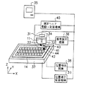
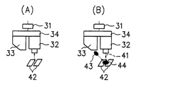
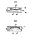
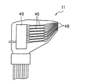
| JP2009194084A (ja) | 電子デバイスあるいは電子回路の製造装置、電子デバイス基板および電子回路基板 | |
| JP2009099916A (ja) | 電子デバイスあるいは電子回路の製造装置、電子デバイス基板および電子回路基板 | |
| CN100490212C (zh) | 有源矩阵型有机el显示体、其制造方法及其制造装置、液晶阵列及其制造方法、以及滤色片衬底、其制造方法及其制造装置 | |
| JP2005081159A (ja) | 機能性基体製造装置ならびに製造される機能性基体 | |
| JP2009272350A (ja) | パターン配列シート、その製造方法、電子デバイスチップ及びその製造方法 | |
| JP2009135460A (ja) | 電子回路基板、電子デバイス基板、電子デバイス基材および電子デバイスあるいは電子回路の製造装置 | |
| JP2009112965A (ja) | 電子デバイスあるいは電子回路の製造方法、電子デバイスあるいは電子回路の製造装置、電子デバイス基板および電子回路基板 | |
| JP2009295936A (ja) | 電子デバイスチップ及びパターン配線シート | |
| JP2009277804A (ja) | パターン配列シート、その製造方法、電子デバイスチップ及びその製造方法 | |
| JP4773691B2 (ja) | フレキシブル機能性素子基板及びその製造装置 | |
| Lim | Inkjet printability of electronic materials important to the manufacture of fully printed OTFTs | |
| JP2004202292A (ja) | 液滴噴射製造装置及び該装置によって製作される基板 | |
| JP2005085474A (ja) | 機能性基体製造装置ならびに製造される機能性基体 | |
| JP2005246242A (ja) | 機能性基体製造装置及びそれにより製造される機能性基体 | |
| JP2005246240A (ja) | 機能性基体製造装置及びそれにより製造される機能性基体 | |
| JP2004202296A (ja) | 液滴噴射製造装置及びそれによって製作される基板 | |
| KR20130046110A (ko) | 유기 박막 트랜지스터 전극, 이의 제조방법 및 이를 이용한 표시소자 | |
| JP2012135745A (ja) | 導体パターン形成方法および導体パターン形成装置 |
Legal Events
| Date | Code | Title | Description |
|---|---|---|---|
| A521 | Request for written amendment filed |
Free format text: JAPANESE INTERMEDIATE CODE: A523 Effective date: 20101104 |
|
| A621 | Written request for application examination |
Free format text: JAPANESE INTERMEDIATE CODE: A621 Effective date: 20101104 |
|
| A131 | Notification of reasons for refusal |
Free format text: JAPANESE INTERMEDIATE CODE: A131 Effective date: 20120131 |
|
| A977 | Report on retrieval |
Free format text: JAPANESE INTERMEDIATE CODE: A971007 Effective date: 20120131 |
|
| A02 | Decision of refusal |
Free format text: JAPANESE INTERMEDIATE CODE: A02 Effective date: 20120605 |