JP2009088334A - Printed circuit board manufacturing method - Google Patents
Printed circuit board manufacturing method Download PDFInfo
- Publication number
- JP2009088334A JP2009088334A JP2007257495A JP2007257495A JP2009088334A JP 2009088334 A JP2009088334 A JP 2009088334A JP 2007257495 A JP2007257495 A JP 2007257495A JP 2007257495 A JP2007257495 A JP 2007257495A JP 2009088334 A JP2009088334 A JP 2009088334A
- Authority
- JP
- Japan
- Prior art keywords
- printed wiring
- wiring board
- sided
- double
- forming
- Prior art date
- Legal status (The legal status is an assumption and is not a legal conclusion. Google has not performed a legal analysis and makes no representation as to the accuracy of the status listed.)
- Granted
Links
Images


Abstract
Description
本発明は、プリント配線板の製造方法に関し、特に貫通孔および/または非貫通孔を用いて層間の電気的接続を行うプリント配線板の製造方法に関する。 The present invention relates to a method for manufacturing a printed wiring board, and more particularly to a method for manufacturing a printed wiring board that performs electrical connection between layers using through holes and / or non-through holes.
近年、電子機器の小型化、多機能化に伴い、機器内部に使用されるプリント配線板の小型化、高密度化が求められている。このような要求に応えるため、プリント配線板に形成される配線回路の微細化、プリント配線板の多層化等が行われる。 In recent years, with the miniaturization and multi-functionalization of electronic devices, there is a demand for miniaturization and high density of printed wiring boards used inside the devices. In order to meet such a demand, miniaturization of a wiring circuit formed on the printed wiring board, multilayering of the printed wiring board, and the like are performed.
多層プリント配線板において層間の電気的接続を行う場合には、一般に、スルーホールやビアホールと呼ばれる、貫通孔や非貫通孔の内壁を電解めっき等によって金属電極層で被覆した構造が用いられる。 When electrical connection between layers is performed in a multilayer printed wiring board, a structure in which inner walls of through holes or non-through holes, which are called through holes or via holes, are covered with a metal electrode layer by electrolytic plating or the like is generally used.
この場合、配線回路形成用の金属電極層上に、さらに電解めっき等による第2の金属電極層が形成されることになるため、配線回路を形成する電極層の総厚みが増加し、微細配線の形成には不利となる。また、電極層の総厚み増加を抑制するために第2の金属電極層を薄く形成することもできるが、その場合、スルーホールやビアホールの内壁に設けられた金属電極層の厚みも薄くなることから、層間の接続信頼性が低下し、断線等の不良に繋がる虞れがある。 In this case, since the second metal electrode layer by electrolytic plating or the like is further formed on the metal electrode layer for forming the wiring circuit, the total thickness of the electrode layer forming the wiring circuit increases, and the fine wiring It is disadvantageous to the formation of. In addition, the second metal electrode layer can be formed thin in order to suppress an increase in the total thickness of the electrode layer, but in this case, the thickness of the metal electrode layer provided on the inner wall of the through hole or via hole is also reduced. Therefore, the connection reliability between the layers is lowered, and there is a possibility that it may lead to defects such as disconnection.
さらに最近、プリント配線板の小型化、高密度化に伴って層間接続を行うスルーホールやビアホールの小径化が進んできており、これに起因する不具合が層間の接続信頼性の低下に拍車をかけている。 In recent years, through-holes and via-holes that make interlayer connections have become smaller in size as printed wiring boards have become smaller and higher in density, and failures caused by this have spurred a decrease in interlayer connection reliability. ing.
このような現状に対し、層間接続部分のみにめっきを厚付けして接続信頼性を確保するボタンめっきと呼ばれる工法が一般に知られている。 In contrast to such a current situation, a method called button plating is generally known in which plating is thickened only at an interlayer connection portion to ensure connection reliability.
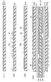
ボタンめっき工法を用いるプリント配線板は、通常、以下の工程により作製されるものである。すなわち、まず、図5(1)に示すように、厚さ25μm程度のポリイミド等の絶縁ベース材51の両面に、厚さ5μm程度の銅箔52を有する両面銅張積層板53を用意する。
A printed wiring board using a button plating method is usually produced by the following steps. That is, first, as shown in FIG. 5A, a double-sided
次に、図5(2)に示すように、両面銅張積層板53に対し、ダイレクトレーザ加工法を用いて直径50μm程度の貫通孔54を形成し、続いて電解めっきにより層間接続を取るための前処理として、デスミア処理、導電化処理を行う。
Next, as shown in FIG. 5 (2), a through-
そして、後にめっきレジストとして利用する感光性ドライフィルム55を積層し、次いで露光、現像を行うことで、貫通孔54およびその周辺部分に感光性ドライフィルムの開口56を形成する。
Then, a photosensitive
次に、図5(3)に示すように、貫通孔54および開口56に対して、電解銅めっき処理を用いて10μm程度の銅めっき層57を形成し、層間の電気的接続を図る。このとき、層間接続部分にのみ電解銅めっき処理を施すことから、層間接続部分の配置によっては電流密度が不安定になり、銅めっき層57の厚みばらつきを低減することが難しい。
Next, as shown in FIG. 5 (3), a
特に、孤立した層間接続部分には電流が集中することから、銅めっき層57の厚さを最大で15μm程度にする必要がある。続いて、感光性ドライフィルム55を剥離することで、層間接続部分にのみめっきが厚付けされた両面銅張積層板53aを得る。
In particular, since current concentrates in isolated interlayer connection portions, the thickness of the
次に、図5(4)に示すように、両面銅張積層板53aの両面にエッチングレジストとして利用する感光性ドライフィルム58を積層し、続いて露光、現像を行う。
Next, as shown in FIG. 5 (4), a photosensitive
このとき、最大で15μm程度の厚さを持つ銅めっき層57の部分をマスクする感光性ドライフィルム58の厚さとしては、20μmもしくはそれ以上が必要となる。このため、薄型の高解像度ドライフィルムを使用することができず、厚く解像性能が低い感光性ドライフィルムを使用することとなる。
At this time, the thickness of the photosensitive
これにより、感光性ドライフィルム58のレジストギャップ58aの幅は、解像性能から考えて24μm以上は必要となり、後のエッチングの追い込み、エッチングばらつき等を考慮すると、安定して形成可能な配線ピッチは60μmもしくはそれ以上に大きくなる。
As a result, the width of the
次に、図5(5)に示すように、通常のサブトラクティブ法によるエッチング手法を用いて銅箔52に配線回路52aを形成し、感光性ドライフィルム58を剥離する。続いてソルダーレジスト層59を形成し、必要に応じて部品実装用ランドやコネクタ等の端子表面に半田めっき、ニッケルめっき、金めっき等の表面処理を施す。
Next, as shown in FIG. 5 (5), a
以上の工程により、層間接続部分のみにめっきが厚付けされた両面プリント配線板53bを得る。
Through the above steps, a double-sided printed
このように、層間接続部分のみにめっきを厚付けするボタンめっき工法を用いたプリント配線板では、高い接続信頼性が得られるものの、配線回路の形成においては薄型の高解像度ドライフィルムが使用できないために微細配線の形成が困難である。さらには、層間接続部に厚付けされためっき厚のばらつきが大きいことから、基板平坦度が低下し、後の部品実装においても問題となることが懸念される。 As described above, a printed wiring board using a button plating method in which plating is applied only to the interlayer connection portion can provide high connection reliability, but a thin high-resolution dry film cannot be used in forming a wiring circuit. However, it is difficult to form fine wiring. Furthermore, since there is a large variation in the thickness of the plating applied to the interlayer connection, there is a concern that the flatness of the substrate will be lowered, causing a problem in subsequent component mounting.
これに対し、高密度な配線を持つ両面プリント配線板を製造するための方法として、特許文献1に、めっきレジストの外側に剥離性の樹脂層を形成し、導電化処理を行った後、前記剥離性の樹脂層を剥離し、その後、電解めっき等により層間接続を行い、続いて配線回路を形成する方法が記載されている。
On the other hand, as a method for producing a double-sided printed wiring board having a high-density wiring, in
しかしながら、このような方法では、スルーホールの内壁に形成された銅めっきと配線パターンとの接触が不十分であり、高い接続信頼性は得られない。加えて、配線回路形成の際にはスルーホールの孔や、銅めっきの突出部等が問題となり、薄型の高解像度ドライフィルムは使用不可能となるため、課題の解決には至らない。 However, in such a method, contact between the copper plating formed on the inner wall of the through hole and the wiring pattern is insufficient, and high connection reliability cannot be obtained. In addition, when forming a wiring circuit, a hole in a through hole, a protruding portion of copper plating, and the like become problems, and a thin high-resolution dry film cannot be used. Therefore, the problem cannot be solved.
また、特許文献2には、めっきレジストを用いて両面プリント配線板の片面側のみに銅めっきを形成する方法が記載されている。これにより、めっき無しとなる片側には微細な配線回路が形成できるとしている。
しかしながら、このような方法では、銅めっきの形成された面には微細配線は形成不能であり、また、スルーホール内壁に形成された銅めっきと、めっき無しとなる配線パターンとの接触が不十分であり、高い接続信頼性は得られない。 However, in such a method, fine wiring cannot be formed on the surface on which the copper plating is formed, and contact between the copper plating formed on the inner wall of the through hole and the wiring pattern without plating is insufficient. Therefore, high connection reliability cannot be obtained.
一方、高密度配線と接続信頼性とを両立させたプリント配線板を製造するための方法として、特許文献3に、エッチングストッパー層となる異種金属層を有する金属箔を用いて、微細配線の形成後にビルドアップ工法を用いて積層する方法が記載されている。
On the other hand, as a method for manufacturing a printed wiring board that achieves both high-density wiring and connection reliability,
しかしながら、このような方法は、両面プリント配線板への応用が困難であり、エッチングストッパー層を有する金属箔を用意する必要があるなど、コスト的にも不利である。 However, such a method is disadvantageous in terms of cost because it is difficult to apply to a double-sided printed wiring board and a metal foil having an etching stopper layer needs to be prepared.
さらに、特許文献4には、導電層だけを選択エッチング可能な異種金属パターンをエッチングレジストとして利用する方法が記載されている。
Further,
しかし、この方法は、片面プリント配線板を想定した方法であり、層間接続構造について何ら言及しておらず、課題の解決には至らない。
上述のように、多層プリント配線板において層間の電気的接続を行う場合には、一般に、スルーホールやビアホールと呼ばれる、貫通孔や非貫通孔の内壁を電解めっき等によって金属電極層で被覆した構造が用いられる。この場合、配線回路形成用の金属電極層上に、さらに電解めっき等による第2の金属電極層が形成されることになるため、配線回路を形成する電極層の総厚みが増加し、微細配線の形成には不利となる。 As described above, when electrical connection between layers is performed in a multilayer printed wiring board, a structure in which the inner wall of a through hole or a non-through hole is generally covered with a metal electrode layer by electrolytic plating or the like, which is called a through hole or a via hole Is used. In this case, since the second metal electrode layer by electrolytic plating or the like is further formed on the metal electrode layer for forming the wiring circuit, the total thickness of the electrode layer forming the wiring circuit increases, and the fine wiring It is disadvantageous to the formation of.
また、電極層の総厚み増加を抑制するため第2の金属電極層を薄く形成することもできるが、その場合、スルーホールやビアホールの孔内壁の金属電極層の厚みも薄くなることから、層間の接続信頼性が低下し、断線等の不良に繋がる虞れがある。これらのことから、高い接続信頼性を確保しながら、微細な配線を形成することが望まれている。 In addition, the second metal electrode layer can be formed thin in order to suppress the increase in the total thickness of the electrode layer, but in this case, the thickness of the metal electrode layer on the inner wall of the through hole or via hole is also reduced. Connection reliability may be reduced, leading to defects such as disconnection. For these reasons, it is desired to form fine wiring while ensuring high connection reliability.
本発明は上述の点を考慮してなされたもので、高い接続信頼性を確保しながら、同時に微細な配線が形成可能であるプリント配線板の製造方法を提供することを目的とする。 The present invention has been made in view of the above points, and an object of the present invention is to provide a method for manufacturing a printed wiring board capable of forming a fine wiring at the same time while ensuring high connection reliability.
上記目的達成のため、本願では、次の発明を提供する。 In order to achieve the above object, the present application provides the following invention.
第一の発明によれば、
絶縁層の両面に導電層を持った両面板の前記導電層に回路を形成する、両面プリント配線板の製造方法であって、
(1) 前記両面板を用意する工程、
(2) 前記両面板に対して、前記導電層とは異なるエッチング特性を持った異種金属のパターンを形成する工程、
(3) 前記両面板に導通用孔を形成する工程、
(4) 前記導通用孔を電解めっき処理することにより、前記導線層間の電気的接続を行う工程、
(5) 前記異種金属のパターンをエッチングレジストとして前記導電層を選択的にエッチングして配線回路を形成する工程、
を含むことを特徴とする。
According to the first invention,
A method of manufacturing a double-sided printed wiring board, wherein a circuit is formed on the conductive layer of a double-sided board having conductive layers on both sides of an insulating layer,
(1) preparing the double-sided board;
(2) A step of forming a pattern of a dissimilar metal having an etching characteristic different from that of the conductive layer on the double-sided plate,
(3) The process of forming the hole for conduction | electrical_connection in the said double-sided board,
(4) A step of performing electrical connection between the conductor layers by subjecting the hole for conduction to electrolytic plating,
(5) forming a wiring circuit by selectively etching the conductive layer using the pattern of the different metal as an etching resist;
It is characterized by including.
また、第二の発明によれば、
2層以上の多層プリント配線板の製造方法であって、
(1) 絶縁層の両面または片面に導電層を有する積層板を用意する工程、
(2) 前記導電層上に、前記導電層とは異なるエッチング特性を持った異種金属のパターンを形成する工程、
(3) プリント配線板を用意する工程、
(4) 前記異種金属のパターンが形成された前記積層板を、層間接着剤を介して前記プリント配線板に積層する工程、
(5) 前記積層板及び前記プリント配線板に導通用孔を形成する工程、
(6) 前記導通用孔を電解めっき処理することにより、前記導電層間の電気的接続を行う工程、
(7) 前記異種金属パターンをエッチングレジストとして前記導電層を選択的にエッチングし配線回路を形成する工程、
を含むことを特徴とする。
According to the second invention,
A method for producing a multilayer printed wiring board having two or more layers,
(1) A step of preparing a laminate having a conductive layer on both sides or one side of an insulating layer,
(2) forming a dissimilar metal pattern having an etching characteristic different from that of the conductive layer on the conductive layer;
(3) a step of preparing a printed wiring board;
(4) A step of laminating the laminated board on which the pattern of the different metal is formed on the printed wiring board via an interlayer adhesive,
(5) forming a conduction hole in the laminate and the printed wiring board;
(6) A step of performing electrical connection between the conductive layers by subjecting the hole for conduction to electrolytic plating,
(7) forming a wiring circuit by selectively etching the conductive layer using the different metal pattern as an etching resist;
It is characterized by including.
これらの特徴により、本発明は次のような効果を奏する。 Due to these features, the present invention has the following effects.
第一の発明によれば、前述の特徴により、高い接続信頼性を確保しながらピッチ25μmの微細配線がプリント配線板の両面に対して安定して形成可能であり、高密度で小型化が可能な両面プリント配線板を安価にかつ安定的に製造することができる。 According to the first invention, due to the above-described features, fine wiring with a pitch of 25 μm can be stably formed on both sides of the printed wiring board while ensuring high connection reliability, and can be miniaturized at high density. A simple double-sided printed wiring board can be manufactured inexpensively and stably.
また第二の発明によれば、前述の特徴により、高い接続信頼性を確保しながら、ピッチ35μmの微細配線が、多層プリント配線板の表面電極層に対して安定して形成可能であり、高密度で小型化が可能な多層プリント配線板を安価にかつ安定的に製造することができる。 Further, according to the second invention, due to the above-described characteristics, fine wiring with a pitch of 35 μm can be stably formed on the surface electrode layer of the multilayer printed wiring board while ensuring high connection reliability. A multilayer printed wiring board that can be reduced in size and density can be manufactured inexpensively and stably.
以下、添付図面を参照して本発明の実施の形態について説明する。 Hereinafter, embodiments of the present invention will be described with reference to the accompanying drawings.
本発明に係るプリント配線板は、貫通孔および/または非貫通孔を用いて層間の電気的接続を行うプリント配線板の製造方法に関する。 The printed wiring board which concerns on this invention is related with the manufacturing method of the printed wiring board which performs an electrical connection between layers using a through-hole and / or a non-through-hole.
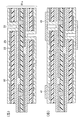
図1A、図1Bおよび図2は、本発明の第一の実施形態におけるプリント配線板の製造工程を示す概念的断面図である。このプリント配線板は、以下の工程により作製されるものである。すなわち、まず、図1A(1)に示す、エポキシ、ポリイミド等からなる厚さ25μm程度の絶縁ベース材1の両面に厚さ5μm程度の銅箔2が設けられた両面銅張積層板3を用意する。ここで用いる銅箔2の厚さは、後に微細配線を形成することから考えて、10μm以下とすることが望ましい。
FIG. 1A, FIG. 1B, and FIG. 2 are conceptual cross-sectional views showing manufacturing steps of the printed wiring board in the first embodiment of the present invention. This printed wiring board is manufactured by the following steps. That is, first, as shown in FIG. 1A (1), a double-sided copper clad
なお、絶縁ベース材1の材質は、エポキシ、ポリイミドに限定されるわけではなく、用途に応じて使い分けることができる。例えば、高速信号伝送時の誘電体損失を低減させる必要があるようなアプリケーションにおいては、低誘電正接材料として液晶ポリマー等をベースとした両面銅張積層板を用いることもできる。また、銅箔2に圧延銅箔を用い、絶縁ベース材1に可撓性のポリイミド等を用いれば、高い屈曲特性を実現することが可能となる。
In addition, the material of the insulating
次に、図1A(2)に示すように、両面銅張積層板3の両面に感光性ドライフィルムを積層し、次いで露光、現像を行うことでマスクパターン4を形成する。この際、両面銅張積層板3の両面は平坦であり、孔等も存在しないから、薄型の高解像度ドライフィルムを使用することで微細なマスクパターン4が形成可能である。
Next, as shown to FIG. 1A (2), the photosensitive dry film is laminated | stacked on both surfaces of the double-sided copper clad laminated
この実施形態1では、5μm厚の高解像度ドライフィルムを用いることで、マスクパターン4の微細配線部4aのパターン幅を8μm、パターンギャップを17μm(ピッチ25μm)に形成した。この程度のパターン幅、パターンギャップであれば、汎用露光機で十分対応可能であり、高価な高精度露光機は必要ではない。
In the first embodiment, by using a high resolution dry film having a thickness of 5 μm, the pattern width of the
次に、図1A(3)に示すように、マスクパターン4の開口部に対し、電解ニッケルめっき処理を用いて1〜3μm程度のニッケル層5を形成する。続いて、マスクパターン4の剥離を行うことで、表面にニッケル層5が形成された両面銅張積層板3aを得る。
Next, as shown in FIG. 1A (3), a
ここで形成するニッケル層5は、後に微細な配線回路を形成する際、エッチングレジストとして利用するためのものである。この実施形態1においては、ニッケル層5の微細配線部5aはニッケルレジスト幅17μm、レジストギャップ8μmとなっている。
The
なお、ここで形成されたレジストギャップは、後に銅箔2をエッチングして微細配線を形成するために用いるから、形成するレジストギャップの厚みは2μm〜20μmの範囲内とするのが望ましく、レジストのパターンピッチは60μm以下とするのが望ましい。
In addition, since the resist gap formed here is used to form the fine wiring by etching the
なお上記工程において、後にエッチングレジストとして用いる材料はニッケルに限定される訳ではなく、銅箔2に対するエッチングレジストとして機能する材料であれば何でもよい。例えば、半田めっき、錫めっき、金めっき等が挙げられる。
In the above process, the material used as an etching resist later is not limited to nickel, and any material that functions as an etching resist for the
ただし、このエッチングレジストは、後に行うデスミア処理に晒されることから、感光性ドライフィルムのような高分子材料は適さない。なお、銅箔界面での耐腐食性、耐熱性、剥離性等を総合的に考慮すると、ニッケルを用いるのが好適と考えられる。 However, since this etching resist is exposed to a desmear process to be performed later, a polymer material such as a photosensitive dry film is not suitable. In consideration of the corrosion resistance, heat resistance, peelability, etc. at the copper foil interface, it is considered preferable to use nickel.
次に、図1A(4)に示すように、UV−YAGレーザ等によるダイレクトレーザ加工法を用いて、後に層間の電気的接続を行うための直径50μm程度の導通用孔を形成し、レーザ処理により発生したスミアを除去するためのデスミア処理を行い、続いて導電化処理を行った後、電解銅めっき処理を用いて10μm厚程度の銅めっき層6を形成し、層間の電気的接続を図る。
Next, as shown in FIG. 1A (4), a direct laser processing method using a UV-YAG laser or the like is used to form a conduction hole having a diameter of about 50 μm for subsequent electrical connection between layers, and laser processing. After performing a desmear process for removing smear generated by the above, followed by a conductive process, a
この際、両面銅張積層板3aの全面に一様に銅めっき層6を形成することができるため、銅めっき層6の厚みばらつきは非常に小さく抑えられる。また、厚さ1〜3μm程度のニッケル層5の凹凸は、上記電解銅めっき処理によってほぼレベリングされて表面は平坦になる。以上の工程により、層間接続の取れた両面銅張積層板3bを得る。
At this time, since the
なお、上記導通用孔の形成手段はUV−YAGレーザに限定される訳ではなく、要求される加工径およびスループット、加工精度、品質等を考慮して、炭酸ガスレーザ加工やドリル加工等を単独でまたは組み合わせて使用することができる。また、この実施形態1では導通用孔を貫通させ、スルーホールを形成しているが、非貫通孔を形成してビアホールを形成することもできる。 Note that the means for forming the hole for conduction is not limited to the UV-YAG laser, and in consideration of the required processing diameter and throughput, processing accuracy, quality, etc., carbon dioxide laser processing and drill processing are performed independently. Or they can be used in combination. In the first embodiment, the through hole is formed through the conduction hole, but the via hole can be formed by forming a non-through hole.
また、銅めっき層6の厚みは、絶縁ベース材1の材質や厚さ、導通用孔の直径、層間接続部の構造、要求される接続信頼性等を考慮して決定されるものであり、10μmには限定されない。より高い接続信頼性が要求される場合には、厚みを増加させて対応することができる。なお、銅めっき層6の厚みを増加させた場合でも、後に形成する微細配線の厚さは銅箔2の厚さで規定されており、微細配線の形成に対して不利になることはない。
The thickness of the
次に、図1B(5)に示すように、両面銅張積層板3bに対して感光性ドライフィルム7を積層し、次いで露光、現像を行うことで層間接続部分やランド等の、銅めっき層6を残す必要がある部分をマスクする。この感光性ドライフィルム7としては、耐アルカリ性のある20μm程度の厚さの感光性ドライフィルムを用いることができる。
Next, as shown in FIG. 1B (5), a photosensitive
次に、図1B(6)に示すように、銅のみを選択的にエッチングすることで、配線回路2aおよび層間接続部のランド6aを形成し、感光性ドライフィルム7の剥離を行う。この際、使用するエッチング液は、ニッケルに対する腐食性が低く、銅を選択的にエッチングするエッチング液、たとえばアンモニアを含むアルカリ性のエッチング液を用いることができる。
Next, as shown in FIG. 1B (6), only the copper is selectively etched to form the
図2は、配線回路2aの微細配線部の拡大図である。配線回路2aを形成するとき、銅箔2の厚みは5μmと薄く、エッチングレジストとして利用するニッケル層5の開口幅8μm(ピッチ25μm)からエッチングを進行させ、片側約3μm程度までエッチングを進行させることにより、パターンギャップを14μm程度に形成する。この程度までエッチングを進行させれば、エッチングばらつきを考慮してもショート等の不良に至る虞れはなく、安定して配線間の絶縁性を確保することができる。
FIG. 2 is an enlarged view of a fine wiring portion of the
これにより、ピッチ25μm(Line/Space=11μm/14μm、パターンTOP=7μm)の微細な配線を、プリント配線板の両面に安定して形成することができる。なおこのとき、配線回路2aには銅めっき層6は含まれないため、銅箔2に圧延銅箔を用い、絶縁ベース材1に可撓性のポリイミド等を用いた場合、高い屈曲特性を実現することができる。
Thereby, fine wiring with a pitch of 25 μm (Line / Space = 11 μm / 14 μm, pattern TOP = 7 μm) can be stably formed on both surfaces of the printed wiring board. At this time, since the
なお、後に部品を実装するに当って、銅めっき層6の厚さ(10μm程度)分の凹凸が問題となる場合には、ランド8のように同じ部品を搭載するランド全てに銅めっき層6を残すのが望ましい。これにより、部品を実装する部分の平坦度が確保され、安定した実装工程を容易に構築できる。
In addition, when the unevenness corresponding to the thickness (about 10 μm) of the
また、製品外周部等の回路とはならない部分についても、銅めっき層6を残すのが望ましい。これにより、両面プリント配線板の電極層が厚くなり、製品の曲げ強さが向上し、後のリフロー等の実装工程において反り等の問題を生じることなく、安定した実装工程を構築できる。
Moreover, it is desirable to leave the
それに加えて、両面プリント配線板全体の寸法収縮を抑え、後のカバー形成や部品実装等の位置合わせにおいても有利となるし、さらには、不要なエッチング液の消耗を抑えることで、コスト的にも有利となる。以上の工程により、微細配線が形成された両面プリント配線板3cを得る。
In addition, the overall size reduction of the double-sided printed wiring board is suppressed, which is advantageous for positioning such as later cover formation and component mounting. Is also advantageous. Through the above steps, the double-sided printed
次に、図1B(7)に示すように、ニッケル層5の剥離を行い、ソルダーレジスト層9を形成し、必要に応じて部品実装用ランドやコネクタ等の端子表面に半田めっき、ニッケルめっき、錫めっき、金めっき等の表面処理を単独でまたは組合わせて施す。
Next, as shown in FIG. 1B (7), the
このとき、ニッケル層5の剥離を行うに当っては、銅に対する腐食性が低く、ニッケルのみを選択的にエッチングするエッチング液、たとえば過酸化水素や硝酸を含むエッチング液を用いることができる。なお、このニッケル層5の剥離は必要不可欠な工程ではなく、後の不良に繋がらないのであれば、特に行わなくてもよい。
At this time, when the
以上の工程により、高い接続信頼性を確保しながら、ピッチ25μm(パターンTOP=7μm、Line/Space=11μm/14μm)の微細配線を、プリント配線板の両面に対して安定して形成可能であり、高密度で小型化が可能な両面プリント配線板を安価にしかも安定的に製造することができる。 Through the above steps, fine wiring with a pitch of 25 μm (pattern TOP = 7 μm, Line / Space = 11 μm / 14 μm) can be stably formed on both sides of the printed wiring board while ensuring high connection reliability. A double-sided printed wiring board that can be miniaturized with high density can be manufactured inexpensively and stably.
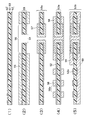
図3Aないし図3Cおよび図4は、本発明の第二の実施形態における多層プリント配線板の製造工程を示す概念的断面図である。本発明の第二の実施形態における多層プリント配線板は、コアとなる両面プリント配線板の片面もしくは両面に、他のプリント配線板をビルドアップすることにより作製される。この第二の実施形態は、ビルドアップ工法を用いる多層プリント配線板であれば、実施することができる。 FIG. 3A to FIG. 3C and FIG. 4 are conceptual cross-sectional views showing the manufacturing process of the multilayer printed wiring board in the second embodiment of the present invention. The multilayer printed wiring board according to the second embodiment of the present invention is produced by building up another printed wiring board on one side or both sides of a double-sided printed wiring board serving as a core. This second embodiment can be implemented as long as it is a multilayer printed wiring board using a build-up method.
まず、図3A(1)に示すように、エポキシ、ポリイミド等からなる厚さ25μm程度の絶縁ベース材21の片面に、厚さ5μm程度の銅箔22を有する片面銅張積層板23を用意する。ここで用いる銅箔22の厚さは、後に微細配線を形成することから考えて、15μm以下とすることが望ましい。
First, as shown in FIG. 3A (1), a single-sided copper clad
次に、図3A(2)に示すように、片面銅張積層板23の銅箔22の側面に感光性ドライフィルムを積層し、次いで露光、現像を行うことで、マスクパターン24を形成する。この際、片面銅張積層板23は平坦であり、孔等も存在しないことから薄型の高解像度ドライフィルムを使用することで微細なマスクパターン24を形成できる。
Next, as shown to FIG. 3A (2), the photosensitive dry film is laminated | stacked on the side surface of the
この実施形態1では、5μm厚の高解像度ドライフィルムを用いることで、マスクパターン24の微細配線部24aのパターン幅を10μm、パターンギャップを25μm(ピッチ35μm)に形成した。この程度のパターン幅、パターンギャップであれば、汎用露光機で十分対応可能であり、高価な高精度露光機は必要ではない。
In the first embodiment, by using a high resolution dry film having a thickness of 5 μm, the pattern width of the
次に、図3A(3)に示すように、マスクパターン24の開口部に対し、電解ニッケルめっき処理を用いて1〜3μm程度のニッケル層25を形成する。ここで形成するニッケル層は、後に微細な配線回路を形成する際、エッチングレジストとして利用するためのものである。この実施形態1においては、ニッケル層25の微細配線部25aはニッケルレジスト幅25μm、レジストギャップ10μmとなっている。
Next, as shown in FIG. 3A (3), a
なお、ここで形成されたレジストギャップから、後に銅箔22をエッチングして微細配線を形成することから、形成するレジストギャップは2μm〜30μmの範囲内とするのが望ましく、レジストのパターンピッチは100μm以下とするのが望ましい。続いてマスクパターン24の剥離を行うことで、表面にニッケル層が形成された片面銅張積層板23aを得る。
Since the
なお、上記工程において、後にエッチングレジストとして用いる材料はニッケルに限定される訳ではなく、銅箔22に対するエッチングレジストとして機能する材料であれば何でもよい。例えば、半田めっき、錫めっき、金めっき等が挙げられる。
In the above process, the material used later as an etching resist is not limited to nickel, and any material that functions as an etching resist for the
ただし、このエッチングレジストは、後に行うデスミア処理に晒されることから、感光性ドライフィルムのような高分子材料は適さない。なお、銅箔界面での耐腐食性、耐熱性、剥離性等を総合的に考慮すると、ニッケルを用いるのが好適と考えられる。 However, since this etching resist is exposed to a desmear process to be performed later, a polymer material such as a photosensitive dry film is not suitable. In consideration of the corrosion resistance, heat resistance, peelability, etc. at the copper foil interface, it is considered preferable to use nickel.
なお、ここで使用する銅張積層板は、片面銅張積層板に限定されず、両面銅張積層板であってもよい。その場合、層間接着剤を介して張り合わされる面は、積層前に配線回路を形成しておく必要がある。 In addition, the copper clad laminated board used here is not limited to a single-sided copper clad laminated board, A double-sided copper clad laminated board may be sufficient. In that case, it is necessary to form a wiring circuit on the surface bonded through the interlayer adhesive before the lamination.
次に、図3A(4)に示すように、配線パターンの形成された両面プリント配線板26の両面に対し、層間接着剤27を介して、片面銅張積層板23aを、位置合わせを行って真空プレス等で積層する。両面プリント配線板26としては、25μm程度の厚さを持つポリイミド等の絶縁ベース材28の両面に、12μm程度の厚さを持つ配線パターン29を有し、ビアフィルめっきで充填した有底ビアホール30により層間接続し、配線パターン29を一般的なカバーレイ30で保護した両面プリント配線板を用いることができる。
Next, as shown in FIG. 3A (4), the single-sided copper-clad
なお、絶縁ベース材28の材質は、ポリイミドに限定される訳ではなく、用途に応じて使い分けることができる。また、両面プリント配線板の層間接続構造は、ビアフィルめっきで充填した有底ビアホールに限定されず、通常の電解めっきを用いた有底ビアホールや、貫通孔を持つスルーホールなど、多種多様な層間接続構造を持つ両面プリント配線板を使用することができる。 Note that the material of the insulating base material 28 is not limited to polyimide, and can be properly used depending on the application. In addition, the interlayer connection structure of the double-sided printed wiring board is not limited to the bottomed via hole filled with via fill plating. A double-sided printed wiring board having a structure can be used.
また、両面プリント配線板の代わりに片面プリント配線板を用いることもできる。層間接着剤27としては、例えば30μm厚のアクリル、エポキシ等の接着剤を使用することができる。以上の工程により、ビルドアップされた多層基材31を得る。
Moreover, a single-sided printed wiring board can be used instead of the double-sided printed wiring board. As the
次に、図3B(5)に示すように、多層基材31の所定の位置に、UV−YAGレーザ等によるダイレクトレーザ加工法を用いて、後に層間の電気的接続を行うための直径100〜150μm程度の導通用孔を形成し、レーザ処理により発生したスミアを除去するためのデスミア処理を行い、続いて導電化処理を行った後、電解銅めっき処理を用いて30μm程度の銅めっき層32を析出させてビアホール33を形成し、層間の電気的接続を図る。
Next, as shown in FIG. 3B (5), a diameter 100 to 100 for performing electrical connection between layers at a predetermined position of the
この際、多層基材31の全面に一様に銅めっき層32を形成することができるため、銅めっき層32の厚みばらつきは非常に小さく抑えられる。また、厚さ1〜3μm程度のニッケル層25の凹凸は、上記電解銅めっき処理によってほぼレベリングされて表面は平坦になる。以上の工程により、層間接続の取れた多層基材31aを得る。
At this time, since the
なお、上記導通用孔の形成はUV−YAGレーザに限定される訳ではなく、要求される加工径およびスループット、加工精度、品質等を考慮して、炭酸ガスレーザ加工やドリル加工等を単独でまたは組み合わせて使用することができる。また、この実施形態2では非貫通の導通用孔を形成し、ビアホールを形成しているが、貫通孔を形成し、スルーホールを形成することもできる。 The formation of the conduction hole is not limited to the UV-YAG laser, and in consideration of the required processing diameter and throughput, processing accuracy, quality, etc., carbon dioxide laser processing, drill processing, etc. are performed alone or Can be used in combination. In the second embodiment, a non-penetrating conduction hole is formed and a via hole is formed. However, a through hole can be formed and a through hole can be formed.
また、銅めっき層32の厚みは、各層の材質や厚さ、導通用孔の直径、層間接続部の構造、要求される接続信頼性等を考慮して決定されるものであり、30μmには限定されない。より高い接続信頼性が要求される場合には、厚みを増加させて対応することができる。なお、銅めっき層32の厚みを増加させた場合でも、後に形成する微細配線の厚さは銅箔22の厚さで規定されており、微細配線の形成に対して不利になることはない。
The thickness of the
次に、図3B(6)に示すように、多層基材31aの両面に感光性ドライフィルム41を積層し、次いで露光、現像を行うことで層間接続部分やランド等の、銅めっき層32を残す必要がある部分をマスクする。感光性ドライフィルム41としては、耐アルカリ性のある20μm程度の厚さの感光性ドライフィルムを用いることができる。
Next, as shown in FIG. 3B (6), a photosensitive
続いて、図3C(7)に示すように、銅のみを選択的にエッチングすることで、配線回路22aおよび層間接続部のランド32aを形成し、感光性ドライフィルム41の剥離を行う。この際、使用するエッチング液は、ニッケルに対する腐食性が低く、銅を選択的にエッチングするエッチング液、たとえばアンモニアを含むアルカリ性のエッチング液を用いることができる。
Subsequently, as shown in FIG. 3C (7), only the copper is selectively etched to form the
ここで、図4は、配線回路22aの微細配線部の拡大図である。配線回路22aを形成するとき、銅箔22の厚みは5μmと薄く、エッチングレジストとして利用するニッケル層25の微細開口幅10μm(開口ピッチ35μm)からエッチングを進行させ、開口幅10μmから片側約4.5μm程度までエッチングを進行させることにより、パターンギャップを19μm程度に形成する。この程度までエッチングを進行させれば、エッチングばらつきを考慮してもショート等の不良に至る虞れはなく、安定して配線間の絶縁性を確保することができる。
Here, FIG. 4 is an enlarged view of a fine wiring portion of the
通常、ビルドアップ工法を行う場合の多層プリント配線板の表層電極層に対して配線回路を形成する場合には、電極層の総厚み以外にも次のような問題がある。 Usually, when a wiring circuit is formed on the surface electrode layer of a multilayer printed wiring board in the case of performing a build-up method, there are the following problems in addition to the total thickness of the electrode layer.
多層プリント配線板は、内層の電極層の有無や、可撓性ケーブル部等の存在により、配線板表面の凹凸が両面プリント配線板に比較して大きい。このため、使用する感光性ドライフィルムは厚く低解像度のものを使用せざるを得ない。また、この表面の凹凸が、露光時のクリアランスに対して誤差となり、露光自体の解像度が低下する。 The multilayer printed wiring board has larger irregularities on the surface of the wiring board than the double-sided printed wiring board due to the presence or absence of an inner electrode layer and the presence of a flexible cable portion. For this reason, the photosensitive dry film to be used must be thick and have a low resolution. Further, the unevenness of the surface becomes an error with respect to the clearance during exposure, and the resolution of the exposure itself is lowered.
これに対し、本発明による多層プリント配線板の配線回路の形成では、ビルドアップ工程の前にニッケル層25によって微細なエッチングレジストを精度よく形成できる。このため、エッチングレジストの形成においては、上記多層プリント配線板の表面の凹凸は問題とはならない。これにより、ピッチ35μm(Line/Space=16μm/19μm、パターンTOP=11μm)の微細な配線を、多層プリント配線板の両面の表層電極層に対して、安定して形成可能である。
On the other hand, in the formation of the wiring circuit of the multilayer printed wiring board according to the present invention, a fine etching resist can be accurately formed by the
このとき、ビアホール33の直径を100μmとすれば、片側25μm程度の露光ずれ、35μm程度のレーザ加工ずれを考慮し、ビアホール上には直径220μm程度のランド32aが形成可能である。ビアホール33に繋がるニッケルパターンのランドは、さらに露光ずれを片側につき25μmだけ考慮して直径270μmに形成すればよい。
At this time, if the diameter of the via
このような微細配線を表層電極層に形成することで、例えば0.4mmピッチの接続ピンを持つCSP等を実装する場合、ランド直径が270μmであるから、ランド間のギャップは130μmとなり、0.4mmピッチの接続ピンの間にピッチ35μmの微細配線を3本も形成することができる。 By forming such fine wiring on the surface electrode layer, for example, when a CSP having a connection pin with a pitch of 0.4 mm is mounted, the land diameter is 270 μm, so the gap between lands is 130 μm. Three fine wirings with a pitch of 35 μm can be formed between connecting pins with a pitch of 4 mm.
このことから、近年求められている狭ピッチな多数の接続ピンを持つ部品を搭載する場合でも、配線の引き回しに余裕が生まれ、延いてはプリント配線板全体の小型化、高密度化へと繋がる。 As a result, even when a component having a large number of connection pins with a narrow pitch, which has been required in recent years, is mounted, there is a margin in the routing of the wiring, which leads to downsizing and higher density of the entire printed wiring board. .
なお、後にビアホール33上にCSP等の部品を実装する場合、銅めっき層32の厚さ(30μm程度)分の凹凸が問題となる可能性がある。そのような場合には、ランド42のように同じ部品を搭載するランド全てに銅めっき層32を残すのが望ましい。これにより、部品を実装する部分の平坦度が確保され、安定した実装工程を容易に構築できる。
Note that when a component such as CSP is mounted on the via
また、製品外周部等の回路とはならない部分についても、銅めっき層32を残すのが望ましい。これにより、多層プリント配線板の表層電極層が厚くなって製品の曲げ強さが向上し、後のリフロー等の実装工程において反り等の問題なく安定した実装工程を構築できる。それに加えて、多層プリント配線板全体の寸法収縮を抑え、後のソルダーレジスト形成や部品実装等の位置合わせにおいても有利となるし、さらには、不要なエッチング液の消耗を抑えることで、コスト的にも有利となる。以上の工程により、微細配線が形成された多層プリント配線板31bを得る。
Moreover, it is desirable to leave the
そして、図3C(8)に示すように、ニッケル層25の剥離を行い、ソルダーレジスト層43を形成し、必要に応じて部品実装用ランドやコネクタ等の端子表面に半田めっき、ニッケルめっき、錫めっき、金めっき等の表面処理を単独でまたは組合わせて施す。
Then, as shown in FIG. 3C (8), the
このとき、ニッケル層25の剥離を行うに当っては、銅に対する腐食性が低く、ニッケルのみを選択的にエッチングするエッチング液、たとえば過酸化水素や硝酸を含むエッチング液を用いることができる。なお、このニッケル層25の剥離は、必要不可欠な工程ではなく、後の不良に繋がらないのであれば、特に行わなくてもよい。
At this time, when the
以上の工程により、高い接続信頼性を確保しながら、ピッチ35μm(パターンTOP=11μm、Line/Space=16μm/19μm)の微細配線が多層プリント配線板の両面の表層電極層に対して安定して形成可能であり、高密度で小型化が可能な多層プリント配線板を安価にかつ安定的に製造することができる。 Through the above steps, fine wiring with a pitch of 35 μm (pattern TOP = 11 μm, Line / Space = 16 μm / 19 μm) is stably provided on the surface electrode layers on both sides of the multilayer printed wiring board while ensuring high connection reliability. A multilayer printed wiring board that can be formed and can be miniaturized at a high density can be manufactured inexpensively and stably.
1 厚さ25μm程度の絶縁ベース材
2 厚さ5μm程度の銅箔
2a 配線回路
3 両面銅張積層板
3a 表面にニッケル層の形成された両面銅張積層板
3b 層間接続のとれた両面銅張積層板
3c 微細配線の形成された両面銅張積層板
4 マスクパターン
4a マスクパターンの微細配線部
5 ニッケル層
5a ニッケル層の微細配線部
6 銅めっき層
6a ランド
7 感光性ドライフィルム
8 ランド
9 ソルダーレジスト
21 厚さ25μm程度の絶縁ベース材
22 厚さ5μm程度の銅箔
22a 配線回路
23 片面銅張積層板
23a 表面にニッケル層の形成された片面銅張積層板
24 マスクパターン
24a マスクパターンの微細配線部
25 ニッケル層
25a ニッケル層の微細配線部
26 両面プリント配線板
27 層間接着剤シート
28 厚さ25μm程度の絶縁ベース材
29 配線パターン
30 ビアホール
31 ビルドアップされた多層基材
31a 層間接続のとれた多層基材
31b 微細配線が形成された多層プリント配線板
32 銅めっき層
32a ランド
33 ビアホール
41 感光性ドライフィルム
42 ランド
43 ソルダーレジスト
51 厚さ25μm程度の絶縁ベース材
52 厚さ5μm程度の銅箔
53 両面銅張積層板
53a 両面銅張積層板
53b 両面プリント配線板
54 貫通孔
55 感光性ドライフィルム
56 感光性ドライフィルムの開口
57 銅めっき層
58 感光性ドライフィルム
58a 感光性ドライフィルムのレジストギャップ
59 ソルダーレジスト
1 Insulating base material having a thickness of about 25 μm 2 Copper foil 2 a having a thickness of about 5 μm Wiring circuit 3 Double-sided copper-clad laminate 3 a Double-sided copper-clad laminate 3 b with a nickel layer formed on the surface Double-sided copper-clad laminate with interlayer connection Plate 3c Double-sided copper-clad laminate 4 with fine wiring formed Mask pattern 4a Mask pattern fine wiring portion 5 Nickel layer 5a Nickel layer fine wiring portion 6 Copper plating layer 6a Land 7 Photosensitive dry film 8 Land 9 Solder resist 21 Insulating base material 22 having a thickness of about 25 μm Copper foil 22a having a thickness of about 5 μm Wiring circuit 23 Single-sided copper-clad laminate 23a Single-sided copper-clad laminate 24 having a nickel layer formed on the surface Mask pattern 24a Fine wiring portion 25 of the mask pattern Nickel layer 25a Fine wiring part 26 of nickel layer Double-sided printed wiring board 27 Interlayer adhesive sheet 28 Thickness of about 25 μm Base material 29 Wiring pattern 30 Via hole 31 Multilayer base material 31a built up Multilayer base material 31b with interlayer connection Multilayer printed wiring board 32 with fine wiring formed Copper plating layer 32a Land 33 Via hole 41 Photosensitive dry film 42 Land 43 Solder resist 51 Insulation base material 52 having a thickness of about 25 μm 52 Copper foil 53 having a thickness of about 5 μm Double-sided copper-clad laminate 53a Double-sided copper-clad laminate 53b Double-sided printed wiring board 54 Through hole 55 Photosensitive dry film 56 Photosensitive dry film Opening 57 copper plating layer 58 photosensitive dry film 58a photosensitive dry film resist gap 59 solder resist
Claims (6)
(1) 前記両面板を用意する工程、
(2) 前記両面板に対して、前記導電層とは異なるエッチング特性を持った異種金属のパターンを形成する工程、
(3) 前記両面板に導通用孔を形成する工程、
(4) 前記導通用孔を電解めっき処理することにより、前記導線層間の電気的接続を行う工程、
(5) 前記異種金属のパターンをエッチングレジストとして前記導電層を選択的にエッチングして配線回路を形成する工程、
を含むことを特徴とする両面プリント配線板の製造方法。 A method of manufacturing a double-sided printed wiring board, wherein a circuit is formed on the conductive layer of a double-sided board having conductive layers on both sides of an insulating layer,
(1) preparing the double-sided board;
(2) A step of forming a pattern of a dissimilar metal having an etching characteristic different from that of the conductive layer on the double-sided plate,
(3) The process of forming the hole for conduction | electrical_connection in the said double-sided board,
(4) A step of performing electrical connection between the conductor layers by subjecting the hole for conduction to electrolytic plating,
(5) forming a wiring circuit by selectively etching the conductive layer using the pattern of the different metal as an etching resist;
The manufacturing method of the double-sided printed wiring board characterized by including.
感光性樹脂材料を用いて前記両面板の両面にマスクパターンを形成し、
めっき処理を用いて前記感光性樹脂材料によりマスクされない部分に前記異種金属のパターンを形成し、
前記感光性樹脂材料を剥離する
ことを特徴とする両面プリント配線板の製造方法。 It is a manufacturing method of the double-sided printed wiring board according to claim 1,
Form a mask pattern on both sides of the double-sided plate using a photosensitive resin material,
Forming a pattern of the dissimilar metal on a portion that is not masked by the photosensitive resin material using a plating process;
The manufacturing method of the double-sided printed wiring board characterized by peeling the said photosensitive resin material.
前記異種金属の層を前記両面板の表面に形成し、
前記感光性樹脂材料を用いて前記異種金属の層の表面にマスクパターンを形成し、
前記異種金属の層を選択的にエッチングしてパターンを形成し、
前記感光性樹脂材料を剥離する
ことを特徴とする両面プリント配線板の製造方法。 In the manufacturing method of the double-sided printed wiring board of Claim 2,
Forming a layer of the dissimilar metal on the surface of the double-sided plate;
Forming a mask pattern on the surface of the layer of the dissimilar metal using the photosensitive resin material;
Selectively etching the layer of dissimilar metal to form a pattern;
The manufacturing method of the double-sided printed wiring board characterized by peeling the said photosensitive resin material.
(1) 絶縁層の両面または片面に導電層を有する積層板を用意する工程、
(2) 前記導電層上に、前記導電層とは異なるエッチング特性を持った異種金属のパターンを形成する工程、
(3) プリント配線板を用意する工程、
(4) 前記異種金属のパターンが形成された前記積層板を、層間接着剤を介して前記プリント配線板に積層する工程、
(5) 前記積層板及び前記プリント配線板に導通用孔を形成する工程、
(6) 前記導通用孔を電解めっき処理することにより、前記導電層間の電気的接続を行う工程、
(7) 前記異種金属パターンをエッチングレジストとして前記導電層を選択的にエッチングし配線回路を形成する工程、
を含むことを特徴とする多層プリント配線板の製造方法。 A method for producing a multilayer printed wiring board having two or more layers,
(1) A step of preparing a laminate having a conductive layer on both sides or one side of an insulating layer,
(2) forming a dissimilar metal pattern having an etching characteristic different from that of the conductive layer on the conductive layer;
(3) a step of preparing a printed wiring board;
(4) A step of laminating the laminated board on which the pattern of the different metal is formed on the printed wiring board via an interlayer adhesive,
(5) forming a conduction hole in the laminate and the printed wiring board;
(6) A step of performing electrical connection between the conductive layers by subjecting the hole for conduction to electrolytic plating,
(7) forming a wiring circuit by selectively etching the conductive layer using the different metal pattern as an etching resist;
A method for producing a multilayer printed wiring board, comprising:
前記積層板の前記導電層上にマスクパターンを形成し、
感光性樹脂材料によりマスクされない部分にめっき処理により前記異種金属のパターンを形成し、
前記感光性樹脂材料を剥離する
ことを特徴とする多層プリント板の製造方法。 In the manufacturing method of the multilayer printed wiring board of Claim 4,
Forming a mask pattern on the conductive layer of the laminate,
Forming a pattern of the dissimilar metal by plating on a portion not masked by the photosensitive resin material;
A method for producing a multilayer printed board, comprising peeling off the photosensitive resin material.
前記積層板の前記導電層上に前記異種金属の層を形成し、
感光性樹脂材料を用いて前記異種金属の層の表面にマスクパターンを形成し、
前記異種金属の層を選択的にエッチングしてパターンを形成し、
前記感光性樹脂材料を剥離する
ことを特徴とする多層プリント配線板の製造方法。 In the manufacturing method of the multilayer printed wiring board of Claim 4,
Forming the dissimilar metal layer on the conductive layer of the laminate;
Form a mask pattern on the surface of the layer of the dissimilar metal using a photosensitive resin material,
Selectively etching the layer of dissimilar metal to form a pattern;
The manufacturing method of the multilayer printed wiring board characterized by peeling the said photosensitive resin material.
Priority Applications (1)
| Application Number | Priority Date | Filing Date | Title |
|---|---|---|---|
| JP2007257495A JP5000446B2 (en) | 2007-10-01 | 2007-10-01 | Method for manufacturing printed wiring board |
Applications Claiming Priority (1)
| Application Number | Priority Date | Filing Date | Title |
|---|---|---|---|
| JP2007257495A JP5000446B2 (en) | 2007-10-01 | 2007-10-01 | Method for manufacturing printed wiring board |
Publications (2)
| Publication Number | Publication Date |
|---|---|
| JP2009088334A true JP2009088334A (en) | 2009-04-23 |
| JP5000446B2 JP5000446B2 (en) | 2012-08-15 |
Family
ID=40661343
Family Applications (1)
| Application Number | Title | Priority Date | Filing Date |
|---|---|---|---|
| JP2007257495A Expired - Fee Related JP5000446B2 (en) | 2007-10-01 | 2007-10-01 | Method for manufacturing printed wiring board |
Country Status (1)
| Country | Link |
|---|---|
| JP (1) | JP5000446B2 (en) |
Cited By (2)
| Publication number | Priority date | Publication date | Assignee | Title |
|---|---|---|---|---|
| CN102256453A (en) * | 2010-05-21 | 2011-11-23 | 富葵精密组件(深圳)有限公司 | Multilayer circuit board manufacturing method |
| CN102548253A (en) * | 2010-12-28 | 2012-07-04 | 富葵精密组件(深圳)有限公司 | Manufacturing method of multilayer circuit board |
Citations (5)
| Publication number | Priority date | Publication date | Assignee | Title |
|---|---|---|---|---|
| JPH077264A (en) * | 1993-06-15 | 1995-01-10 | Nec Toyama Ltd | Manufacture of printed wiring board |
| JPH07235752A (en) * | 1994-02-24 | 1995-09-05 | Hitachi Chem Co Ltd | Method for removing chlolrine ion from etching solution and wiring board producing methods using this solution |
| JP2000195985A (en) * | 1998-12-24 | 2000-07-14 | Shinko Electric Ind Co Ltd | Manufacture of substrate for semiconductor device |
| JP2001036217A (en) * | 1999-07-21 | 2001-02-09 | Ngk Spark Plug Co Ltd | Manufacture of wiring board and etching device |
| JP2002539630A (en) * | 1999-03-16 | 2002-11-19 | シーメンス アクチエンゲゼルシヤフト | Method for providing contact holes in an electrically insulated base material having metal layers on both sides |
-
2007
- 2007-10-01 JP JP2007257495A patent/JP5000446B2/en not_active Expired - Fee Related
Patent Citations (5)
| Publication number | Priority date | Publication date | Assignee | Title |
|---|---|---|---|---|
| JPH077264A (en) * | 1993-06-15 | 1995-01-10 | Nec Toyama Ltd | Manufacture of printed wiring board |
| JPH07235752A (en) * | 1994-02-24 | 1995-09-05 | Hitachi Chem Co Ltd | Method for removing chlolrine ion from etching solution and wiring board producing methods using this solution |
| JP2000195985A (en) * | 1998-12-24 | 2000-07-14 | Shinko Electric Ind Co Ltd | Manufacture of substrate for semiconductor device |
| JP2002539630A (en) * | 1999-03-16 | 2002-11-19 | シーメンス アクチエンゲゼルシヤフト | Method for providing contact holes in an electrically insulated base material having metal layers on both sides |
| JP2001036217A (en) * | 1999-07-21 | 2001-02-09 | Ngk Spark Plug Co Ltd | Manufacture of wiring board and etching device |
Cited By (2)
| Publication number | Priority date | Publication date | Assignee | Title |
|---|---|---|---|---|
| CN102256453A (en) * | 2010-05-21 | 2011-11-23 | 富葵精密组件(深圳)有限公司 | Multilayer circuit board manufacturing method |
| CN102548253A (en) * | 2010-12-28 | 2012-07-04 | 富葵精密组件(深圳)有限公司 | Manufacturing method of multilayer circuit board |
Also Published As
| Publication number | Publication date |
|---|---|
| JP5000446B2 (en) | 2012-08-15 |
Similar Documents
| Publication | Publication Date | Title |
|---|---|---|
| JP5198105B2 (en) | Manufacturing method of multilayer flexible printed wiring board | |
| JPH04309290A (en) | Manufacture of printed circuit board | |
| JP2007128970A (en) | Manufacturing method of multilayer wiring board having cable section | |
| WO2018110437A1 (en) | Wiring substrate, multilayer wiring substrate, and method for manufacturing wiring substrate | |
| JP2009260204A (en) | Printed circuit board and method of manufacturing the same | |
| JP2008016482A (en) | Manufacturing method of multilayer printed wiring board | |
| KR101009176B1 (en) | A fabricating method of multilayer printed circuit board | |
| KR100832650B1 (en) | Multi layer printed circuit board and fabricating method of the same | |
| JP2005236067A (en) | Wiring substrate, its manufacturing method and semiconductor package | |
| JP2013106034A (en) | Manufacturing method of printed circuit board | |
| KR102046006B1 (en) | High-current transfer methods utilizing the printed circuit board | |
| JP5000446B2 (en) | Method for manufacturing printed wiring board | |
| JP2010034430A (en) | Wiring board and method for manufacturing the same | |
| CN110366310B (en) | Soft and hard composite board and its making method | |
| JP2010016061A (en) | Printed wiring board, and manufacturing method therefor | |
| KR100658972B1 (en) | Pcb and method of manufacturing thereof | |
| KR101108816B1 (en) | Multilayer printed circuit substrate and method of manufacturing the same | |
| JP2000165045A (en) | Printed wiring board | |
| TW201446099A (en) | Method for manufacturing printed circuit board | |
| JP2006128291A (en) | Multilayered printed wiring board, manufacturing method thereof and electronic device | |
| JP2003273510A (en) | Manufacturing method for printed substrate | |
| JP2009088337A (en) | Printed circuit board and its manufacturing method | |
| JP2006005040A (en) | Wiring board, magnetic disk device, and method for manufacturing the wiring board | |
| JP5062533B2 (en) | Wiring board manufacturing method | |
| KR101085576B1 (en) | Method for fabricating printed-circuit-board using metal and printed-circuit-board fabricated using thereof |
Legal Events
| Date | Code | Title | Description |
|---|---|---|---|
| A621 | Written request for application examination |
Free format text: JAPANESE INTERMEDIATE CODE: A621 Effective date: 20100705 |
|
| A131 | Notification of reasons for refusal |
Free format text: JAPANESE INTERMEDIATE CODE: A131 Effective date: 20111118 |
|
| A977 | Report on retrieval |
Free format text: JAPANESE INTERMEDIATE CODE: A971007 Effective date: 20111124 |
|
| A521 | Written amendment |
Free format text: JAPANESE INTERMEDIATE CODE: A523 Effective date: 20111228 |
|
| A131 | Notification of reasons for refusal |
Free format text: JAPANESE INTERMEDIATE CODE: A131 Effective date: 20120120 |
|
| A521 | Written amendment |
Free format text: JAPANESE INTERMEDIATE CODE: A523 Effective date: 20120215 |
|
| TRDD | Decision of grant or rejection written | ||
| A01 | Written decision to grant a patent or to grant a registration (utility model) |
Free format text: JAPANESE INTERMEDIATE CODE: A01 Effective date: 20120420 |
|
| A01 | Written decision to grant a patent or to grant a registration (utility model) |
Free format text: JAPANESE INTERMEDIATE CODE: A01 |
|
| A61 | First payment of annual fees (during grant procedure) |
Free format text: JAPANESE INTERMEDIATE CODE: A61 Effective date: 20120516 |
|
| R150 | Certificate of patent or registration of utility model |
Free format text: JAPANESE INTERMEDIATE CODE: R150 |
|
| FPAY | Renewal fee payment (event date is renewal date of database) |
Free format text: PAYMENT UNTIL: 20150525 Year of fee payment: 3 |
|
| R250 | Receipt of annual fees |
Free format text: JAPANESE INTERMEDIATE CODE: R250 |
|
| R250 | Receipt of annual fees |
Free format text: JAPANESE INTERMEDIATE CODE: R250 |
|
| R250 | Receipt of annual fees |
Free format text: JAPANESE INTERMEDIATE CODE: R250 |
|
| LAPS | Cancellation because of no payment of annual fees |