JP2008198667A - 半導体製造装置及び半導体装置の製造方法 - Google Patents
半導体製造装置及び半導体装置の製造方法 Download PDFInfo
- Publication number
- JP2008198667A JP2008198667A JP2007029787A JP2007029787A JP2008198667A JP 2008198667 A JP2008198667 A JP 2008198667A JP 2007029787 A JP2007029787 A JP 2007029787A JP 2007029787 A JP2007029787 A JP 2007029787A JP 2008198667 A JP2008198667 A JP 2008198667A
- Authority
- JP
- Japan
- Prior art keywords
- support device
- wafer
- axis
- brush
- roller
- Prior art date
- Legal status (The legal status is an assumption and is not a legal conclusion. Google has not performed a legal analysis and makes no representation as to the accuracy of the status listed.)
- Pending
Links
- 238000004519 manufacturing process Methods 0.000 title claims abstract description 56
- 239000004065 semiconductor Substances 0.000 title claims abstract description 55
- 238000004140 cleaning Methods 0.000 claims description 114
- NJPPVKZQTLUDBO-UHFFFAOYSA-N novaluron Chemical compound C1=C(Cl)C(OC(F)(F)C(OC(F)(F)F)F)=CC=C1NC(=O)NC(=O)C1=C(F)C=CC=C1F NJPPVKZQTLUDBO-UHFFFAOYSA-N 0.000 claims description 14
- 230000002093 peripheral effect Effects 0.000 claims description 12
- 238000000034 method Methods 0.000 claims description 11
- 238000000638 solvent extraction Methods 0.000 claims description 3
- 235000012431 wafers Nutrition 0.000 description 131
- 239000000758 substrate Substances 0.000 description 40
- 239000007788 liquid Substances 0.000 description 7
- 238000009434 installation Methods 0.000 description 3
- 210000000078 claw Anatomy 0.000 description 2
- 238000001035 drying Methods 0.000 description 2
- 238000005192 partition Methods 0.000 description 2
- 239000007921 spray Substances 0.000 description 2
- 239000000356 contaminant Substances 0.000 description 1
- 239000010419 fine particle Substances 0.000 description 1
- 239000012535 impurity Substances 0.000 description 1
- 239000002184 metal Substances 0.000 description 1
- 239000005416 organic matter Substances 0.000 description 1
Images


Classifications
-
- H—ELECTRICITY
- H01—ELECTRIC ELEMENTS
- H01L—SEMICONDUCTOR DEVICES NOT COVERED BY CLASS H10
- H01L21/00—Processes or apparatus adapted for the manufacture or treatment of semiconductor or solid state devices or of parts thereof
- H01L21/02—Manufacture or treatment of semiconductor devices or of parts thereof
- H01L21/02041—Cleaning
- H01L21/02057—Cleaning during device manufacture
-
- B08B1/32—
-
- H—ELECTRICITY
- H01—ELECTRIC ELEMENTS
- H01L—SEMICONDUCTOR DEVICES NOT COVERED BY CLASS H10
- H01L21/00—Processes or apparatus adapted for the manufacture or treatment of semiconductor or solid state devices or of parts thereof
- H01L21/02—Manufacture or treatment of semiconductor devices or of parts thereof
- H01L21/02041—Cleaning
- H01L21/02082—Cleaning product to be cleaned
- H01L21/0209—Cleaning of wafer backside
-
- H—ELECTRICITY
- H01—ELECTRIC ELEMENTS
- H01L—SEMICONDUCTOR DEVICES NOT COVERED BY CLASS H10
- H01L21/00—Processes or apparatus adapted for the manufacture or treatment of semiconductor or solid state devices or of parts thereof
- H01L21/67—Apparatus specially adapted for handling semiconductor or electric solid state devices during manufacture or treatment thereof; Apparatus specially adapted for handling wafers during manufacture or treatment of semiconductor or electric solid state devices or components ; Apparatus not specifically provided for elsewhere
- H01L21/67005—Apparatus not specifically provided for elsewhere
- H01L21/67011—Apparatus for manufacture or treatment
- H01L21/67017—Apparatus for fluid treatment
- H01L21/67028—Apparatus for fluid treatment for cleaning followed by drying, rinsing, stripping, blasting or the like
- H01L21/6704—Apparatus for fluid treatment for cleaning followed by drying, rinsing, stripping, blasting or the like for wet cleaning or washing
- H01L21/67046—Apparatus for fluid treatment for cleaning followed by drying, rinsing, stripping, blasting or the like for wet cleaning or washing using mainly scrubbing means, e.g. brushes
-
- H—ELECTRICITY
- H01—ELECTRIC ELEMENTS
- H01L—SEMICONDUCTOR DEVICES NOT COVERED BY CLASS H10
- H01L21/00—Processes or apparatus adapted for the manufacture or treatment of semiconductor or solid state devices or of parts thereof
- H01L21/67—Apparatus specially adapted for handling semiconductor or electric solid state devices during manufacture or treatment thereof; Apparatus specially adapted for handling wafers during manufacture or treatment of semiconductor or electric solid state devices or components ; Apparatus not specifically provided for elsewhere
- H01L21/683—Apparatus specially adapted for handling semiconductor or electric solid state devices during manufacture or treatment thereof; Apparatus specially adapted for handling wafers during manufacture or treatment of semiconductor or electric solid state devices or components ; Apparatus not specifically provided for elsewhere for supporting or gripping
- H01L21/687—Apparatus specially adapted for handling semiconductor or electric solid state devices during manufacture or treatment thereof; Apparatus specially adapted for handling wafers during manufacture or treatment of semiconductor or electric solid state devices or components ; Apparatus not specifically provided for elsewhere for supporting or gripping using mechanical means, e.g. chucks, clamps or pinches
- H01L21/68714—Apparatus specially adapted for handling semiconductor or electric solid state devices during manufacture or treatment thereof; Apparatus specially adapted for handling wafers during manufacture or treatment of semiconductor or electric solid state devices or components ; Apparatus not specifically provided for elsewhere for supporting or gripping using mechanical means, e.g. chucks, clamps or pinches the wafers being placed on a susceptor, stage or support
- H01L21/68728—Apparatus specially adapted for handling semiconductor or electric solid state devices during manufacture or treatment thereof; Apparatus specially adapted for handling wafers during manufacture or treatment of semiconductor or electric solid state devices or components ; Apparatus not specifically provided for elsewhere for supporting or gripping using mechanical means, e.g. chucks, clamps or pinches the wafers being placed on a susceptor, stage or support characterised by a plurality of separate clamping members, e.g. clamping fingers
Abstract
【解決手段】半導体製造装置(1、1’)は、第1支持装置(18)と、前記第1支持装置に固定されたウェハ(30)を洗浄する第1ブラシ(24)と、第2支持装置(4)と、前記第2支持装置に支持されたウェハ(30)を洗浄する第2ブラシ(8、11、8’、11’)とを具備する。前記第1支持装置は、ウェハ(30)が固定された状態で回転する。前記第2支持装置は、ウェハ(30)の周縁部に接触してウェハを回転させるローラー(7)を備える。前記第1支持装置及び前記第2支持装置は、互いに接近及び離隔する。
【選択図】図2
Description
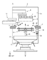
図1は、本発明の第1の実施形態に係る半導体製造装置1の側面図を示している。半導体製造装置1は、チャンバ2と、シャッタ3と、両面洗浄用ウェハ支持装置4と、上ブラシ8と、下ブラシ11と、ノズル14〜17と、片面洗浄用ウェハ支持装置18と、ブラシ24と、カバー27とを備えている。図1及び後述する図2乃至6には、互いに垂直なX、Y、Z方向が示されている。Z方向は、例えば、鉛直方向である。X、Y方向は、例えば、互いに垂直な水平方向である。シャッタ3は、チャンバ2を上側2a及び下側2bに仕切るように設けられ、開閉可能である。上側2aはZ方向上側に配置され、下側2bは、Z方向下側に配置されている。半導体製造装置1は、上側2aにおいて前工程から受け取ったウェハ30の両面を洗浄した後、下側2bにおいてウェハ30の片面を洗浄し、ウェハ30を乾燥して次工程に受け渡す。
本発明の第2の実施形態に係る半導体製造装置1’について以下に説明する。半導体製造装置1’は、半導体製造装置1と同様に、チャンバ2と、シャッタ3と、両面洗浄用ウェハ支持装置4と、ノズル14〜17と、片面洗浄用ウェハ支持装置18と、ブラシ24と、カバー27とを備えている。これらの構成及び動作は、半導体製造装置1の場合と同様である。
2…チャンバ
2a…上側
2b…下側
3…シャッタ
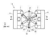
4…両面洗浄用ウェハ支持装置
5、6…ローラー台座
7…ローラー
8、8’…上ブラシ
9、9’…ブラシ本体
10、10’…アーム
11、11’…下ブラシ
12、12’…ブラシ本体
13、13’…アーム
14、15、16、17…ノズル
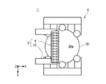
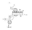
18…片面洗浄用ウェハ支持装置
19、20…回転体
21…固定支持体
22…可動支持体
22a…当接部
23…リンク
24…ブラシ
25…ブラシ本体
26…アーム
27…カバー
30…ウェハ
30a…表面
30b…裏面
40〜46…矢印
Claims (12)
- 第1支持装置と、
前記第1支持装置に固定されたウェハを洗浄する第1ブラシと、
第2支持装置と、
前記第2支持装置に支持されたウェハを洗浄する第2ブラシと
を具備し、
前記第1支持装置は、ウェハが固定された状態で回転し、
前記第2支持装置は、ウェハの周縁部に接触してウェハを回転させるローラーを備え、
前記第1支持装置及び前記第2支持装置は、互いに接近及び離隔する
半導体製造装置。 - 前記第1支持装置は、第1軸まわりに回転し、
前記第1支持装置及び前記第2支持装置は、前記第1軸の方向に沿って接近及び離隔する
請求項1に記載の半導体製造装置。 - 前記第2支持装置は、前記ローラーを含む第1ローラー群が取り付けられた第1ローラー台座と、第2ローラー群が取り付けられた第2ローラー台座とを備え、
前記第1ローラー群及び前記第2ローラー群に含まれる各ローラーは、前記第1軸に平行なローラー回転軸まわりに回転し、
前記第1ローラー台座及び前記第2ローラー台座は、前記第1軸に垂直な方向に沿って接近及び離隔する
請求項2に記載の半導体製造装置。 - 前記第1支持装置は、前記第1軸まわりに回転する第1回転体と、前記第1回転体に対して前記第1軸まわりに回転可能なように前記第1回転体に支持された第2回転体と、複数の可動支持体と、前記複数の可動支持体と前記第2回転体とを接続するリンクとを備え、
前記複数の可動支持体の各々は、前記第1回転体に対して前記第1軸に平行な可動支持体回転軸まわりに回転可能なように前記第1回転体に支持され、前記可動支持体回転軸からずれた位置に設けられウェハの周縁部に当接する当接部を備え、
前記当接部は、前記第1軸を中心軸とする円周上に配置され、
前記リンクは、前記第2回転体の前記第1回転体に対する正逆回転に対応して前記円周が縮径及び拡径するように前記複数の可動支持体を動かし、
前記第1支持装置は、前記第1軸に沿って移動する
請求項2又は3に記載の半導体製造装置。 - 前記第2ブラシは、前記第2支持装置に支持されたウェハの前記第1支持装置を向く面を洗浄可能なブラシ本体と、前記ブラシ本体を支持するアームとを備え、
前記アームは、前記第1軸に垂直な揺動軸まわりに揺動し、
前記第1軸の方向は鉛直方向である
請求項2乃至4のいずれかに記載の半導体製造装置。 - チャンバーと、
前記チャンバーを第1の側と第2の側とに仕切り、開閉可能なシャッターと
を具備し、
前記第1ブラシがウェハを洗浄するときは、前記第1支持装置及び前記第1ブラシが前記第1の側に位置し、
前記第2ブラシがウェハを洗浄するときは、前記第2支持装置及び前記第2ブラシが前記第2の側に位置する
請求項1乃至5のいずれかに記載の半導体製造装置。 - 半導体製造装置を用いる半導体装置の製造方法であって、
前記半導体製造装置は、
ウェハが固定された状態で回転する第1支持装置と、
前記ウェハの周縁部に接触して前記ウェハを回転させるローラーを備えた第2支持装置と
を具備し、
前記半導体装置の製造方法は、
前記第2支持装置に支持された前記ウェハを洗浄する工程と、
前記第1支持装置と前記第2支持装置とを接近させる工程と、
前記第2支持装置から前記第1支持装置に前記ウェハを受け渡す工程と
を具備する
半導体装置の製造方法。 - 前記第1支持装置は、第1軸まわりに回転し、
前記半導体装置の製造方法は、
前記第1支持装置と前記第2支持装置とを接近させる前記工程において、前記第1支持装置と前記第2支持装置とを前記第1軸の方向に沿って接近させる
請求項7に記載の半導体装置の製造方法。 - 前記第2支持装置は、前記ローラーを含む第1ローラー群が取り付けられた第1ローラー台座と、第2ローラー群が取り付けられた第2ローラー台座とを備え、
前記第1ローラー群及び前記第2ローラー群に含まれる各ローラーは、前記第1軸に平行なローラー回転軸まわりに回転し、
前記第2支持装置から前記第1支持装置に前記ウェハを受け渡す前記工程において、前記第1ローラー台座及び前記第2ローラー台座を前記第1軸に垂直な方向に沿って離隔して前記ウェハを解放する
請求項8に記載の半導体装置の製造方法。 - 前記第1支持装置は、前記第1軸まわりに回転する第1回転体と、前記第1回転体に対して前記第1軸まわりに回転可能なように前記第1回転体に支持された第2回転体と、複数の可動支持体と、前記複数の可動支持体と前記第2回転体とを接続するリンクとを備え、
前記複数の可動支持体の各々は、前記第1回転体に対して前記第1軸に平行な可動支持体回転軸まわりに回転可能なように前記第1回転体に支持され、前記可動支持体回転軸からずれた位置に設けられた当接部を備え、
前記当接部は、前記第1軸を中心軸とする円周上に配置され、
前記リンクは、前記第2回転体の前記第1回転体に対する正逆回転に対応して前記円周が縮径及び拡径するように前記複数の可動支持体を動かし、
前記半導体装置の製造方法は、
前記第2回転体を前記第1回転体に対して回転させることで前記当接部を前記ウェハの周縁部に当接させて前記ウェハを前記第1支持装置に固定する工程を具備し、
前記第1支持装置と前記第2支持装置とを接近させる前記工程において、前記第1支持装置を前記第1軸の方向に沿って移動する
請求項8又は9に記載の半導体装置の製造方法。 - 前記半導体製造装置は、
前記第2支持装置に支持された前記ウェハの前記第1支持装置を向く面を洗浄可能なブラシ本体と、
前記ブラシ本体を支持するアームとを備え、
前記第1軸の方向は鉛直方向であり、
前記半導体装置の製造方法は、
前記アームを前記第1軸に垂直な揺動軸まわりに揺動して前記ブラシ本体及び前記アームを前記第1支持装置と前記第2支持装置に支持された前記ウェハとの間から退避させる工程を具備する
請求項8乃至10のいずれかに記載の半導体装置の製造方法。 - 前記半導体製造装置は、
チャンバーと、
前記チャンバーを第1の側と第2の側とに仕切り、開閉可能なシャッターと
を具備し、
前記半導体装置の製造方法は、
前記第1支持装置と前記第2支持装置とを離隔させる工程と、
前記第1支持装置に固定された前記ウェハを洗浄する工程と
を具備し、
前記第2支持装置に支持された前記ウエハを洗浄する前記工程において、前記第2支持装置を前記第2の側に配置し、
前記第1支持装置に固定された前記ウェハを洗浄する前記工程において、前記第1支持装置を前記第1の側に配置する
請求項7乃至11のいずれかに記載の半導体装置の製造方法。
Priority Applications (2)
| Application Number | Priority Date | Filing Date | Title |
|---|---|---|---|
| JP2007029787A JP2008198667A (ja) | 2007-02-08 | 2007-02-08 | 半導体製造装置及び半導体装置の製造方法 |
| US12/028,225 US20080190451A1 (en) | 2007-02-08 | 2008-02-08 | Semiconductor manufacturing apparatus and method for manufacturing semiconductor device |
Applications Claiming Priority (1)
| Application Number | Priority Date | Filing Date | Title |
|---|---|---|---|
| JP2007029787A JP2008198667A (ja) | 2007-02-08 | 2007-02-08 | 半導体製造装置及び半導体装置の製造方法 |
Publications (2)
| Publication Number | Publication Date |
|---|---|
| JP2008198667A true JP2008198667A (ja) | 2008-08-28 |
| JP2008198667A5 JP2008198667A5 (ja) | 2010-03-04 |
Family
ID=39684794
Family Applications (1)
| Application Number | Title | Priority Date | Filing Date |
|---|---|---|---|
| JP2007029787A Pending JP2008198667A (ja) | 2007-02-08 | 2007-02-08 | 半導体製造装置及び半導体装置の製造方法 |
Country Status (2)
| Country | Link |
|---|---|
| US (1) | US20080190451A1 (ja) |
| JP (1) | JP2008198667A (ja) |
Cited By (1)
| Publication number | Priority date | Publication date | Assignee | Title |
|---|---|---|---|---|
| KR101415983B1 (ko) | 2012-12-24 | 2014-07-08 | 주식회사 케이씨텍 | 웨이퍼 세정장치 |
Families Citing this family (4)
| Publication number | Priority date | Publication date | Assignee | Title |
|---|---|---|---|---|
| WO2009065757A1 (en) * | 2007-11-23 | 2009-05-28 | Sez Ag | Device and process for wet treating a peripheral area of a wafer-shaped article |
| US8844546B2 (en) * | 2008-10-01 | 2014-09-30 | Applied Materials, Inc. | Apparatus and method for cleaning semiconductor substrate using pressurized fluid |
| JP5535687B2 (ja) * | 2010-03-01 | 2014-07-02 | 株式会社荏原製作所 | 基板洗浄方法及び基板洗浄装置 |
| CN102909185A (zh) * | 2012-10-26 | 2013-02-06 | 世成电子(深圳)有限公司 | 一种清洁机 |
Citations (4)
| Publication number | Priority date | Publication date | Assignee | Title |
|---|---|---|---|---|
| JPH0637077A (ja) * | 1992-05-18 | 1994-02-10 | Tokyo Electron Ltd | 処理装置 |
| JP2000176386A (ja) * | 1998-12-16 | 2000-06-27 | Ebara Corp | 基板洗浄装置 |
| JP2001179188A (ja) * | 1999-12-22 | 2001-07-03 | Shimada Phys & Chem Ind Co Ltd | ディスク洗浄方法及びそれを使用したディスク洗浄装置 |
| JP2003031541A (ja) * | 2001-07-18 | 2003-01-31 | Speedfam Co Ltd | 洗浄装置 |
Family Cites Families (4)
| Publication number | Priority date | Publication date | Assignee | Title |
|---|---|---|---|---|
| JP3549141B2 (ja) * | 1997-04-21 | 2004-08-04 | 大日本スクリーン製造株式会社 | 基板処理装置および基板保持装置 |
| US6293855B1 (en) * | 1998-03-09 | 2001-09-25 | Ebara Corporation | Polishing apparatus |
| US6622334B1 (en) * | 2000-03-29 | 2003-09-23 | International Business Machines Corporation | Wafer edge cleaning utilizing polish pad material |
| US6932558B2 (en) * | 2002-07-03 | 2005-08-23 | Kung Chris Wu | Wafer aligner |
-
2007
- 2007-02-08 JP JP2007029787A patent/JP2008198667A/ja active Pending
-
2008
- 2008-02-08 US US12/028,225 patent/US20080190451A1/en not_active Abandoned
Patent Citations (4)
| Publication number | Priority date | Publication date | Assignee | Title |
|---|---|---|---|---|
| JPH0637077A (ja) * | 1992-05-18 | 1994-02-10 | Tokyo Electron Ltd | 処理装置 |
| JP2000176386A (ja) * | 1998-12-16 | 2000-06-27 | Ebara Corp | 基板洗浄装置 |
| JP2001179188A (ja) * | 1999-12-22 | 2001-07-03 | Shimada Phys & Chem Ind Co Ltd | ディスク洗浄方法及びそれを使用したディスク洗浄装置 |
| JP2003031541A (ja) * | 2001-07-18 | 2003-01-31 | Speedfam Co Ltd | 洗浄装置 |
Cited By (1)
| Publication number | Priority date | Publication date | Assignee | Title |
|---|---|---|---|---|
| KR101415983B1 (ko) | 2012-12-24 | 2014-07-08 | 주식회사 케이씨텍 | 웨이퍼 세정장치 |
Also Published As
| Publication number | Publication date |
|---|---|
| US20080190451A1 (en) | 2008-08-14 |
Similar Documents
| Publication | Publication Date | Title |
|---|---|---|
| US11192147B2 (en) | Substrate processing apparatus and substrate processing method | |
| JP5904169B2 (ja) | 基板洗浄装置、基板洗浄方法及び記憶媒体 | |
| US9050634B2 (en) | Substrate processing apparatus | |
| JP5606471B2 (ja) | 基板回転保持装置および基板処理装置 | |
| US10926376B2 (en) | Method and apparatus for polishing a substrate, and method for processing a substrate | |
| JP2011071477A (ja) | 液処理装置および液処理方法 | |
| TWI593040B (zh) | 基板處理方法、基板處理系統及記憶有基板處理程式之電腦可讀取記憶媒體 | |
| JP2008198667A (ja) | 半導体製造装置及び半導体装置の製造方法 | |
| US8851769B2 (en) | Substrate processing method | |
| US6560809B1 (en) | Substrate cleaning apparatus | |
| WO2019102868A1 (ja) | 基板搬送装置、基板処理システム、基板処理方法及びコンピュータ記憶媒体 | |
| JP2017108113A (ja) | 基板処理装置および基板処理方法ならびに基板処理装置の制御プログラム | |
| JP6625461B2 (ja) | 研磨装置 | |
| WO2019138881A1 (ja) | 洗浄装置、洗浄方法及びコンピュータ記憶媒体 | |
| CN100362629C (zh) | 半导体晶片的清洗方法 | |
| US11361979B2 (en) | Substrate processing apparatus and substrate processing method | |
| JP5241317B2 (ja) | クリーニング装置 | |
| JP3964517B2 (ja) | 洗浄装置とその方法 | |
| EP3396707B1 (en) | Apparatus and method for cleaning a back surface of a substrate | |
| JP2006332386A (ja) | 基板洗浄装置及び基板洗浄方法 | |
| JP2006196507A (ja) | ウエーハの洗浄装置 | |
| JPH06163491A (ja) | 半導体基板の洗浄方法および洗浄装置 | |
| JP3179571B2 (ja) | ウェハ貼付プレートの洗浄および移送装置 | |
| US10651057B2 (en) | Apparatus and method for cleaning a back surface of a substrate | |
| CN108857858A (zh) | 清洗基板的背面的装置和方法、背面清洗装置和基板处理装置 |
Legal Events
| Date | Code | Title | Description |
|---|---|---|---|
| A521 | Request for written amendment filed |
Free format text: JAPANESE INTERMEDIATE CODE: A523 Effective date: 20100115 |
|
| A621 | Written request for application examination |
Free format text: JAPANESE INTERMEDIATE CODE: A621 Effective date: 20100115 |
|
| A977 | Report on retrieval |
Free format text: JAPANESE INTERMEDIATE CODE: A971007 Effective date: 20110624 |
|
| A131 | Notification of reasons for refusal |
Free format text: JAPANESE INTERMEDIATE CODE: A131 Effective date: 20110628 |
|
| A02 | Decision of refusal |
Free format text: JAPANESE INTERMEDIATE CODE: A02 Effective date: 20111205 |