JP2008176095A - パターン形成方法及び薄膜トランジスタの作製方法 - Google Patents
パターン形成方法及び薄膜トランジスタの作製方法 Download PDFInfo
- Publication number
- JP2008176095A JP2008176095A JP2007009926A JP2007009926A JP2008176095A JP 2008176095 A JP2008176095 A JP 2008176095A JP 2007009926 A JP2007009926 A JP 2007009926A JP 2007009926 A JP2007009926 A JP 2007009926A JP 2008176095 A JP2008176095 A JP 2008176095A
- Authority
- JP
- Japan
- Prior art keywords
- layer
- light
- mask
- light absorption
- laser beam
- Prior art date
- Legal status (The legal status is an assumption and is not a legal conclusion. Google has not performed a legal analysis and makes no representation as to the accuracy of the status listed.)
- Withdrawn
Links
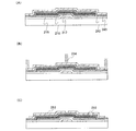
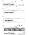
- 238000000034 method Methods 0.000 title claims abstract description 164
- 239000010409 thin film Substances 0.000 title claims abstract description 87
- 238000004519 manufacturing process Methods 0.000 title claims description 34
- 239000000758 substrate Substances 0.000 claims abstract description 110
- 238000005530 etching Methods 0.000 claims abstract description 47
- 230000031700 light absorption Effects 0.000 claims description 158
- 239000004065 semiconductor Substances 0.000 claims description 145
- 239000000463 material Substances 0.000 claims description 104
- 239000010408 film Substances 0.000 claims description 40
- 230000001678 irradiating effect Effects 0.000 claims description 20
- 230000008569 process Effects 0.000 abstract description 26
- 238000007599 discharging Methods 0.000 abstract description 2
- 229920002120 photoresistant polymer Polymers 0.000 abstract description 2
- 239000007788 liquid Substances 0.000 abstract 1
- 230000003287 optical effect Effects 0.000 description 36
- 239000000126 substance Substances 0.000 description 32
- 239000012535 impurity Substances 0.000 description 28
- 239000004973 liquid crystal related substance Substances 0.000 description 19
- 150000002894 organic compounds Chemical class 0.000 description 19
- 150000001875 compounds Chemical class 0.000 description 17
- 239000002585 base Substances 0.000 description 15
- 239000010949 copper Substances 0.000 description 15
- 230000007261 regionalization Effects 0.000 description 15
- -1 tungsten nitride Chemical class 0.000 description 15
- 239000011230 binding agent Substances 0.000 description 14
- 229920005989 resin Polymers 0.000 description 14
- 239000011347 resin Substances 0.000 description 14
- 229910010272 inorganic material Inorganic materials 0.000 description 13
- 229910052757 nitrogen Inorganic materials 0.000 description 10
- RYGMFSIKBFXOCR-UHFFFAOYSA-N Copper Chemical compound [Cu] RYGMFSIKBFXOCR-UHFFFAOYSA-N 0.000 description 9
- VYPSYNLAJGMNEJ-UHFFFAOYSA-N Silicium dioxide Chemical compound O=[Si]=O VYPSYNLAJGMNEJ-UHFFFAOYSA-N 0.000 description 9
- 229910052782 aluminium Inorganic materials 0.000 description 9
- 229910052802 copper Inorganic materials 0.000 description 9
- 238000001704 evaporation Methods 0.000 description 9
- 229910052751 metal Inorganic materials 0.000 description 9
- 239000002184 metal Substances 0.000 description 9
- 238000003672 processing method Methods 0.000 description 9
- XAGFODPZIPBFFR-UHFFFAOYSA-N aluminium Chemical compound [Al] XAGFODPZIPBFFR-UHFFFAOYSA-N 0.000 description 8
- 239000003990 capacitor Substances 0.000 description 8
- 238000001312 dry etching Methods 0.000 description 8
- 238000002347 injection Methods 0.000 description 8
- 239000007924 injection Substances 0.000 description 8
- 150000002484 inorganic compounds Chemical class 0.000 description 8
- 229910052741 iridium Inorganic materials 0.000 description 8
- GKOZUEZYRPOHIO-UHFFFAOYSA-N iridium atom Chemical compound [Ir] GKOZUEZYRPOHIO-UHFFFAOYSA-N 0.000 description 8
- 239000011159 matrix material Substances 0.000 description 8
- 239000002245 particle Substances 0.000 description 8
- 239000005083 Zinc sulfide Substances 0.000 description 7
- 239000011651 chromium Substances 0.000 description 7
- KPUWHANPEXNPJT-UHFFFAOYSA-N disiloxane Chemical class [SiH3]O[SiH3] KPUWHANPEXNPJT-UHFFFAOYSA-N 0.000 description 7
- 238000000206 photolithography Methods 0.000 description 7
- 229910052984 zinc sulfide Inorganic materials 0.000 description 7
- 229910052581 Si3N4 Inorganic materials 0.000 description 6
- XUIMIQQOPSSXEZ-UHFFFAOYSA-N Silicon Chemical compound [Si] XUIMIQQOPSSXEZ-UHFFFAOYSA-N 0.000 description 6
- QVQLCTNNEUAWMS-UHFFFAOYSA-N barium oxide Chemical compound [Ba]=O QVQLCTNNEUAWMS-UHFFFAOYSA-N 0.000 description 6
- 230000008901 benefit Effects 0.000 description 6
- 239000000460 chlorine Substances 0.000 description 6
- 229910052804 chromium Inorganic materials 0.000 description 6
- 230000008020 evaporation Effects 0.000 description 6
- 230000005525 hole transport Effects 0.000 description 6
- 229910052710 silicon Inorganic materials 0.000 description 6
- 239000010703 silicon Substances 0.000 description 6
- HQVNEWCFYHHQES-UHFFFAOYSA-N silicon nitride Chemical compound N12[Si]34N5[Si]62N3[Si]51N64 HQVNEWCFYHHQES-UHFFFAOYSA-N 0.000 description 6
- 229910052814 silicon oxide Inorganic materials 0.000 description 6
- 239000010936 titanium Substances 0.000 description 6
- SPDPTFAJSFKAMT-UHFFFAOYSA-N 1-n-[4-[4-(n-[4-(3-methyl-n-(3-methylphenyl)anilino)phenyl]anilino)phenyl]phenyl]-4-n,4-n-bis(3-methylphenyl)-1-n-phenylbenzene-1,4-diamine Chemical compound CC1=CC=CC(N(C=2C=CC(=CC=2)N(C=2C=CC=CC=2)C=2C=CC(=CC=2)C=2C=CC(=CC=2)N(C=2C=CC=CC=2)C=2C=CC(=CC=2)N(C=2C=C(C)C=CC=2)C=2C=C(C)C=CC=2)C=2C=C(C)C=CC=2)=C1 SPDPTFAJSFKAMT-UHFFFAOYSA-N 0.000 description 5
- PXHVJJICTQNCMI-UHFFFAOYSA-N Nickel Chemical compound [Ni] PXHVJJICTQNCMI-UHFFFAOYSA-N 0.000 description 5
- OAICVXFJPJFONN-UHFFFAOYSA-N Phosphorus Chemical compound [P] OAICVXFJPJFONN-UHFFFAOYSA-N 0.000 description 5
- BQCADISMDOOEFD-UHFFFAOYSA-N Silver Chemical compound [Ag] BQCADISMDOOEFD-UHFFFAOYSA-N 0.000 description 5
- GWEVSGVZZGPLCZ-UHFFFAOYSA-N Titan oxide Chemical compound O=[Ti]=O GWEVSGVZZGPLCZ-UHFFFAOYSA-N 0.000 description 5
- XLOMVQKBTHCTTD-UHFFFAOYSA-N Zinc monoxide Chemical compound [Zn]=O XLOMVQKBTHCTTD-UHFFFAOYSA-N 0.000 description 5
- CUJRVFIICFDLGR-UHFFFAOYSA-N acetylacetonate Chemical compound CC(=O)[CH-]C(C)=O CUJRVFIICFDLGR-UHFFFAOYSA-N 0.000 description 5
- 229910052799 carbon Inorganic materials 0.000 description 5
- 238000005229 chemical vapour deposition Methods 0.000 description 5
- 239000013078 crystal Substances 0.000 description 5
- 239000000428 dust Substances 0.000 description 5
- 239000007789 gas Substances 0.000 description 5
- 239000011521 glass Substances 0.000 description 5
- 239000010931 gold Substances 0.000 description 5
- 239000011147 inorganic material Substances 0.000 description 5
- 239000011777 magnesium Substances 0.000 description 5
- 239000011368 organic material Substances 0.000 description 5
- 229910052709 silver Inorganic materials 0.000 description 5
- 239000004332 silver Substances 0.000 description 5
- 238000010532 solid phase synthesis reaction Methods 0.000 description 5
- 230000005236 sound signal Effects 0.000 description 5
- 238000004544 sputter deposition Methods 0.000 description 5
- 238000000859 sublimation Methods 0.000 description 5
- 230000008022 sublimation Effects 0.000 description 5
- WUPHOULIZUERAE-UHFFFAOYSA-N 3-(oxolan-2-yl)propanoic acid Chemical compound OC(=O)CCC1CCCO1 WUPHOULIZUERAE-UHFFFAOYSA-N 0.000 description 4
- IJGRMHOSHXDMSA-UHFFFAOYSA-N Atomic nitrogen Chemical compound N#N IJGRMHOSHXDMSA-UHFFFAOYSA-N 0.000 description 4
- VYZAMTAEIAYCRO-UHFFFAOYSA-N Chromium Chemical compound [Cr] VYZAMTAEIAYCRO-UHFFFAOYSA-N 0.000 description 4
- JMASRVWKEDWRBT-UHFFFAOYSA-N Gallium nitride Chemical compound [Ga]#N JMASRVWKEDWRBT-UHFFFAOYSA-N 0.000 description 4
- UFHFLCQGNIYNRP-UHFFFAOYSA-N Hydrogen Chemical compound [H][H] UFHFLCQGNIYNRP-UHFFFAOYSA-N 0.000 description 4
- ZOKXTWBITQBERF-UHFFFAOYSA-N Molybdenum Chemical compound [Mo] ZOKXTWBITQBERF-UHFFFAOYSA-N 0.000 description 4
- 239000004642 Polyimide Substances 0.000 description 4
- 239000007983 Tris buffer Substances 0.000 description 4
- XHCLAFWTIXFWPH-UHFFFAOYSA-N [O-2].[O-2].[O-2].[O-2].[O-2].[V+5].[V+5] Chemical compound [O-2].[O-2].[O-2].[O-2].[O-2].[V+5].[V+5] XHCLAFWTIXFWPH-UHFFFAOYSA-N 0.000 description 4
- 125000005595 acetylacetonate group Chemical group 0.000 description 4
- 229910052980 cadmium sulfide Inorganic materials 0.000 description 4
- 239000000919 ceramic Substances 0.000 description 4
- 238000001514 detection method Methods 0.000 description 4
- 230000000694 effects Effects 0.000 description 4
- 230000005684 electric field Effects 0.000 description 4
- 238000010304 firing Methods 0.000 description 4
- PCHJSUWPFVWCPO-UHFFFAOYSA-N gold Chemical compound [Au] PCHJSUWPFVWCPO-UHFFFAOYSA-N 0.000 description 4
- 229910052737 gold Inorganic materials 0.000 description 4
- 239000001257 hydrogen Substances 0.000 description 4
- 229910052739 hydrogen Inorganic materials 0.000 description 4
- 238000000608 laser ablation Methods 0.000 description 4
- 239000007791 liquid phase Substances 0.000 description 4
- 239000003550 marker Substances 0.000 description 4
- 238000002844 melting Methods 0.000 description 4
- 230000008018 melting Effects 0.000 description 4
- 229910052750 molybdenum Inorganic materials 0.000 description 4
- 239000011733 molybdenum Substances 0.000 description 4
- 229910000476 molybdenum oxide Inorganic materials 0.000 description 4
- 150000004767 nitrides Chemical class 0.000 description 4
- 229920003986 novolac Polymers 0.000 description 4
- PQQKPALAQIIWST-UHFFFAOYSA-N oxomolybdenum Chemical compound [Mo]=O PQQKPALAQIIWST-UHFFFAOYSA-N 0.000 description 4
- 229910052698 phosphorus Inorganic materials 0.000 description 4
- 239000011574 phosphorus Substances 0.000 description 4
- 229920001721 polyimide Polymers 0.000 description 4
- 230000006798 recombination Effects 0.000 description 4
- 238000005215 recombination Methods 0.000 description 4
- 230000009467 reduction Effects 0.000 description 4
- 239000000243 solution Substances 0.000 description 4
- 229910001935 vanadium oxide Inorganic materials 0.000 description 4
- 238000001039 wet etching Methods 0.000 description 4
- DRDVZXDWVBGGMH-UHFFFAOYSA-N zinc;sulfide Chemical compound [S-2].[Zn+2] DRDVZXDWVBGGMH-UHFFFAOYSA-N 0.000 description 4
- SKJCKYVIQGBWTN-UHFFFAOYSA-N (4-hydroxyphenyl) methanesulfonate Chemical compound CS(=O)(=O)OC1=CC=C(O)C=C1 SKJCKYVIQGBWTN-UHFFFAOYSA-N 0.000 description 3
- PFNQVRZLDWYSCW-UHFFFAOYSA-N (fluoren-9-ylideneamino) n-naphthalen-1-ylcarbamate Chemical compound C12=CC=CC=C2C2=CC=CC=C2C1=NOC(=O)NC1=CC=CC2=CC=CC=C12 PFNQVRZLDWYSCW-UHFFFAOYSA-N 0.000 description 3
- POXIZPBFFUKMEQ-UHFFFAOYSA-N 2-cyanoethenylideneazanide Chemical group [N-]=C=[C+]C#N POXIZPBFFUKMEQ-UHFFFAOYSA-N 0.000 description 3
- 229910018072 Al 2 O 3 Inorganic materials 0.000 description 3
- JBRZTFJDHDCESZ-UHFFFAOYSA-N AsGa Chemical compound [As]#[Ga] JBRZTFJDHDCESZ-UHFFFAOYSA-N 0.000 description 3
- UHOVQNZJYSORNB-UHFFFAOYSA-N Benzene Chemical compound C1=CC=CC=C1 UHOVQNZJYSORNB-UHFFFAOYSA-N 0.000 description 3
- MSDMPJCOOXURQD-UHFFFAOYSA-N C545T Chemical compound C1=CC=C2SC(C3=CC=4C=C5C6=C(C=4OC3=O)C(C)(C)CCN6CCC5(C)C)=NC2=C1 MSDMPJCOOXURQD-UHFFFAOYSA-N 0.000 description 3
- ZAMOUSCENKQFHK-UHFFFAOYSA-N Chlorine atom Chemical compound [Cl] ZAMOUSCENKQFHK-UHFFFAOYSA-N 0.000 description 3
- 229910052691 Erbium Inorganic materials 0.000 description 3
- PXGOKWXKJXAPGV-UHFFFAOYSA-N Fluorine Chemical compound FF PXGOKWXKJXAPGV-UHFFFAOYSA-N 0.000 description 3
- 229910002601 GaN Inorganic materials 0.000 description 3
- 229910001218 Gallium arsenide Inorganic materials 0.000 description 3
- 229910052779 Neodymium Inorganic materials 0.000 description 3
- UCKMPCXJQFINFW-UHFFFAOYSA-N Sulphide Chemical compound [S-2] UCKMPCXJQFINFW-UHFFFAOYSA-N 0.000 description 3
- 229910052775 Thulium Inorganic materials 0.000 description 3
- RTAQQCXQSZGOHL-UHFFFAOYSA-N Titanium Chemical compound [Ti] RTAQQCXQSZGOHL-UHFFFAOYSA-N 0.000 description 3
- 238000010521 absorption reaction Methods 0.000 description 3
- QVGXLLKOCUKJST-UHFFFAOYSA-N atomic oxygen Chemical compound [O] QVGXLLKOCUKJST-UHFFFAOYSA-N 0.000 description 3
- CJDPJFRMHVXWPT-UHFFFAOYSA-N barium sulfide Chemical compound [S-2].[Ba+2] CJDPJFRMHVXWPT-UHFFFAOYSA-N 0.000 description 3
- UMIVXZPTRXBADB-UHFFFAOYSA-N benzocyclobutene Chemical compound C1=CC=C2CCC2=C1 UMIVXZPTRXBADB-UHFFFAOYSA-N 0.000 description 3
- 230000005540 biological transmission Effects 0.000 description 3
- 239000000872 buffer Substances 0.000 description 3
- 229910052791 calcium Inorganic materials 0.000 description 3
- 239000011575 calcium Substances 0.000 description 3
- 229910052801 chlorine Inorganic materials 0.000 description 3
- 229910052731 fluorine Inorganic materials 0.000 description 3
- 239000011737 fluorine Substances 0.000 description 3
- 229910052733 gallium Inorganic materials 0.000 description 3
- 229910052744 lithium Inorganic materials 0.000 description 3
- 229910052749 magnesium Inorganic materials 0.000 description 3
- 229910044991 metal oxide Inorganic materials 0.000 description 3
- 150000004706 metal oxides Chemical class 0.000 description 3
- 239000000203 mixture Substances 0.000 description 3
- 239000004570 mortar (masonry) Substances 0.000 description 3
- TWNQGVIAIRXVLR-UHFFFAOYSA-N oxo(oxoalumanyloxy)alumane Chemical compound O=[Al]O[Al]=O TWNQGVIAIRXVLR-UHFFFAOYSA-N 0.000 description 3
- SIWVEOZUMHYXCS-UHFFFAOYSA-N oxo(oxoyttriooxy)yttrium Chemical compound O=[Y]O[Y]=O SIWVEOZUMHYXCS-UHFFFAOYSA-N 0.000 description 3
- 229910052760 oxygen Inorganic materials 0.000 description 3
- 239000001301 oxygen Substances 0.000 description 3
- RVTZCBVAJQQJTK-UHFFFAOYSA-N oxygen(2-);zirconium(4+) Chemical compound [O-2].[O-2].[Zr+4] RVTZCBVAJQQJTK-UHFFFAOYSA-N 0.000 description 3
- 238000000059 patterning Methods 0.000 description 3
- 238000005268 plasma chemical vapour deposition Methods 0.000 description 3
- 229920000642 polymer Polymers 0.000 description 3
- 230000005855 radiation Effects 0.000 description 3
- 238000003746 solid phase reaction Methods 0.000 description 3
- 239000002904 solvent Substances 0.000 description 3
- 238000003860 storage Methods 0.000 description 3
- VEALVRVVWBQVSL-UHFFFAOYSA-N strontium titanate Chemical compound [Sr+2].[O-][Ti]([O-])=O VEALVRVVWBQVSL-UHFFFAOYSA-N 0.000 description 3
- 125000001424 substituent group Chemical group 0.000 description 3
- 229910052719 titanium Inorganic materials 0.000 description 3
- 229910052721 tungsten Inorganic materials 0.000 description 3
- 239000010937 tungsten Substances 0.000 description 3
- 229910001928 zirconium oxide Inorganic materials 0.000 description 3
- POILWHVDKZOXJZ-ARJAWSKDSA-M (z)-4-oxopent-2-en-2-olate Chemical compound C\C([O-])=C\C(C)=O POILWHVDKZOXJZ-ARJAWSKDSA-M 0.000 description 2
- UHXOHPVVEHBKKT-UHFFFAOYSA-N 1-(2,2-diphenylethenyl)-4-[4-(2,2-diphenylethenyl)phenyl]benzene Chemical group C=1C=C(C=2C=CC(C=C(C=3C=CC=CC=3)C=3C=CC=CC=3)=CC=2)C=CC=1C=C(C=1C=CC=CC=1)C1=CC=CC=C1 UHXOHPVVEHBKKT-UHFFFAOYSA-N 0.000 description 2
- IYZMXHQDXZKNCY-UHFFFAOYSA-N 1-n,1-n-diphenyl-4-n,4-n-bis[4-(n-phenylanilino)phenyl]benzene-1,4-diamine Chemical compound C1=CC=CC=C1N(C=1C=CC(=CC=1)N(C=1C=CC(=CC=1)N(C=1C=CC=CC=1)C=1C=CC=CC=1)C=1C=CC(=CC=1)N(C=1C=CC=CC=1)C=1C=CC=CC=1)C1=CC=CC=C1 IYZMXHQDXZKNCY-UHFFFAOYSA-N 0.000 description 2
- BFTIPCRZWILUIY-UHFFFAOYSA-N 2,5,8,11-tetratert-butylperylene Chemical group CC(C)(C)C1=CC(C2=CC(C(C)(C)C)=CC=3C2=C2C=C(C=3)C(C)(C)C)=C3C2=CC(C(C)(C)C)=CC3=C1 BFTIPCRZWILUIY-UHFFFAOYSA-N 0.000 description 2
- ZVFQEOPUXVPSLB-UHFFFAOYSA-N 3-(4-tert-butylphenyl)-4-phenyl-5-(4-phenylphenyl)-1,2,4-triazole Chemical compound C1=CC(C(C)(C)C)=CC=C1C(N1C=2C=CC=CC=2)=NN=C1C1=CC=C(C=2C=CC=CC=2)C=C1 ZVFQEOPUXVPSLB-UHFFFAOYSA-N 0.000 description 2
- DHDHJYNTEFLIHY-UHFFFAOYSA-N 4,7-diphenyl-1,10-phenanthroline Chemical compound C1=CC=CC=C1C1=CC=NC2=C1C=CC1=C(C=3C=CC=CC=3)C=CN=C21 DHDHJYNTEFLIHY-UHFFFAOYSA-N 0.000 description 2
- AWXGSYPUMWKTBR-UHFFFAOYSA-N 4-carbazol-9-yl-n,n-bis(4-carbazol-9-ylphenyl)aniline Chemical compound C12=CC=CC=C2C2=CC=CC=C2N1C1=CC=C(N(C=2C=CC(=CC=2)N2C3=CC=CC=C3C3=CC=CC=C32)C=2C=CC(=CC=2)N2C3=CC=CC=C3C3=CC=CC=C32)C=C1 AWXGSYPUMWKTBR-UHFFFAOYSA-N 0.000 description 2
- 229920000178 Acrylic resin Polymers 0.000 description 2
- 239000004925 Acrylic resin Substances 0.000 description 2
- PIGFYZPCRLYGLF-UHFFFAOYSA-N Aluminum nitride Chemical compound [Al]#N PIGFYZPCRLYGLF-UHFFFAOYSA-N 0.000 description 2
- XKRFYHLGVUSROY-UHFFFAOYSA-N Argon Chemical compound [Ar] XKRFYHLGVUSROY-UHFFFAOYSA-N 0.000 description 2
- ZOXJGFHDIHLPTG-UHFFFAOYSA-N Boron Chemical compound [B] ZOXJGFHDIHLPTG-UHFFFAOYSA-N 0.000 description 2
- 229910004261 CaF 2 Inorganic materials 0.000 description 2
- 101000837344 Homo sapiens T-cell leukemia translocation-altered gene protein Proteins 0.000 description 2
- 229920000877 Melamine resin Polymers 0.000 description 2
- ZCQWOFVYLHDMMC-UHFFFAOYSA-N Oxazole Chemical compound C1=COC=N1 ZCQWOFVYLHDMMC-UHFFFAOYSA-N 0.000 description 2
- 229920001609 Poly(3,4-ethylenedioxythiophene) Polymers 0.000 description 2
- 229910004298 SiO 2 Inorganic materials 0.000 description 2
- 229910004283 SiO 4 Inorganic materials 0.000 description 2
- 102100028692 T-cell leukemia translocation-altered gene protein Human genes 0.000 description 2
- 229910052769 Ytterbium Inorganic materials 0.000 description 2
- 229910052783 alkali metal Inorganic materials 0.000 description 2
- 229910000272 alkali metal oxide Inorganic materials 0.000 description 2
- VSCWAEJMTAWNJL-UHFFFAOYSA-K aluminium trichloride Chemical compound Cl[Al](Cl)Cl VSCWAEJMTAWNJL-UHFFFAOYSA-K 0.000 description 2
- 229910021417 amorphous silicon Inorganic materials 0.000 description 2
- 229910052785 arsenic Inorganic materials 0.000 description 2
- RQNWIZPPADIBDY-UHFFFAOYSA-N arsenic atom Chemical compound [As] RQNWIZPPADIBDY-UHFFFAOYSA-N 0.000 description 2
- 125000004429 atom Chemical group 0.000 description 2
- NWAIGJYBQQYSPW-UHFFFAOYSA-N azanylidyneindigane Chemical compound [In]#N NWAIGJYBQQYSPW-UHFFFAOYSA-N 0.000 description 2
- JRPBQTZRNDNNOP-UHFFFAOYSA-N barium titanate Chemical compound [Ba+2].[Ba+2].[O-][Ti]([O-])([O-])[O-] JRPBQTZRNDNNOP-UHFFFAOYSA-N 0.000 description 2
- 229910002113 barium titanate Inorganic materials 0.000 description 2
- 239000004305 biphenyl Substances 0.000 description 2
- 229910052796 boron Inorganic materials 0.000 description 2
- JGIATAMCQXIDNZ-UHFFFAOYSA-N calcium sulfide Chemical compound [Ca]=S JGIATAMCQXIDNZ-UHFFFAOYSA-N 0.000 description 2
- 150000001722 carbon compounds Chemical class 0.000 description 2
- 230000001413 cellular effect Effects 0.000 description 2
- 238000000975 co-precipitation Methods 0.000 description 2
- 239000004020 conductor Substances 0.000 description 2
- 125000002147 dimethylamino group Chemical group [H]C([H])([H])N(*)C([H])([H])[H] 0.000 description 2
- NKZSPGSOXYXWQA-UHFFFAOYSA-N dioxido(oxo)titanium;lead(2+) Chemical compound [Pb+2].[O-][Ti]([O-])=O NKZSPGSOXYXWQA-UHFFFAOYSA-N 0.000 description 2
- 239000002019 doping agent Substances 0.000 description 2
- 239000003822 epoxy resin Substances 0.000 description 2
- VQCBHWLJZDBHOS-UHFFFAOYSA-N erbium(iii) oxide Chemical compound O=[Er]O[Er]=O VQCBHWLJZDBHOS-UHFFFAOYSA-N 0.000 description 2
- 125000001153 fluoro group Chemical group F* 0.000 description 2
- 229910052839 forsterite Inorganic materials 0.000 description 2
- 150000004820 halides Chemical class 0.000 description 2
- 150000002366 halogen compounds Chemical class 0.000 description 2
- 238000010438 heat treatment Methods 0.000 description 2
- 238000003384 imaging method Methods 0.000 description 2
- 239000011261 inert gas Substances 0.000 description 2
- 239000011810 insulating material Substances 0.000 description 2
- 239000012212 insulator Substances 0.000 description 2
- IDBFBDSKYCUNPW-UHFFFAOYSA-N lithium nitride Chemical compound [Li]N([Li])[Li] IDBFBDSKYCUNPW-UHFFFAOYSA-N 0.000 description 2
- FUJCRWPEOMXPAD-UHFFFAOYSA-N lithium oxide Chemical compound [Li+].[Li+].[O-2] FUJCRWPEOMXPAD-UHFFFAOYSA-N 0.000 description 2
- 229910001947 lithium oxide Inorganic materials 0.000 description 2
- HCWCAKKEBCNQJP-UHFFFAOYSA-N magnesium orthosilicate Chemical compound [Mg+2].[Mg+2].[O-][Si]([O-])([O-])[O-] HCWCAKKEBCNQJP-UHFFFAOYSA-N 0.000 description 2
- 239000011572 manganese Substances 0.000 description 2
- 230000007246 mechanism Effects 0.000 description 2
- 239000013081 microcrystal Substances 0.000 description 2
- 238000002156 mixing Methods 0.000 description 2
- 229910052759 nickel Inorganic materials 0.000 description 2
- 229910000480 nickel oxide Inorganic materials 0.000 description 2
- 229910017464 nitrogen compound Inorganic materials 0.000 description 2
- 150000002830 nitrogen compounds Chemical class 0.000 description 2
- QGLKJKCYBOYXKC-UHFFFAOYSA-N nonaoxidotritungsten Chemical compound O=[W]1(=O)O[W](=O)(=O)O[W](=O)(=O)O1 QGLKJKCYBOYXKC-UHFFFAOYSA-N 0.000 description 2
- 125000000962 organic group Chemical group 0.000 description 2
- GNRSAWUEBMWBQH-UHFFFAOYSA-N oxonickel Chemical compound [Ni]=O GNRSAWUEBMWBQH-UHFFFAOYSA-N 0.000 description 2
- DYIZHKNUQPHNJY-UHFFFAOYSA-N oxorhenium Chemical compound [Re]=O DYIZHKNUQPHNJY-UHFFFAOYSA-N 0.000 description 2
- 150000002927 oxygen compounds Chemical class 0.000 description 2
- BPUBBGLMJRNUCC-UHFFFAOYSA-N oxygen(2-);tantalum(5+) Chemical compound [O-2].[O-2].[O-2].[O-2].[O-2].[Ta+5].[Ta+5] BPUBBGLMJRNUCC-UHFFFAOYSA-N 0.000 description 2
- YRZZLAGRKZIJJI-UHFFFAOYSA-N oxyvanadium phthalocyanine Chemical compound [V+2]=O.C12=CC=CC=C2C(N=C2[N-]C(C3=CC=CC=C32)=N2)=NC1=NC([C]1C=CC=CC1=1)=NC=1N=C1[C]3C=CC=CC3=C2[N-]1 YRZZLAGRKZIJJI-UHFFFAOYSA-N 0.000 description 2
- 230000000737 periodic effect Effects 0.000 description 2
- 230000010363 phase shift Effects 0.000 description 2
- 239000005011 phenolic resin Substances 0.000 description 2
- 239000003504 photosensitizing agent Substances 0.000 description 2
- 238000005240 physical vapour deposition Methods 0.000 description 2
- 229920000647 polyepoxide Polymers 0.000 description 2
- 229920001709 polysilazane Polymers 0.000 description 2
- 125000002924 primary amino group Chemical group [H]N([H])* 0.000 description 2
- 238000007639 printing Methods 0.000 description 2
- LLHKCFNBLRBOGN-UHFFFAOYSA-N propylene glycol methyl ether acetate Chemical compound COCC(C)OC(C)=O LLHKCFNBLRBOGN-UHFFFAOYSA-N 0.000 description 2
- 229910003449 rhenium oxide Inorganic materials 0.000 description 2
- 239000010979 ruby Substances 0.000 description 2
- 229910001750 ruby Inorganic materials 0.000 description 2
- 238000007650 screen-printing Methods 0.000 description 2
- 239000003566 sealing material Substances 0.000 description 2
- 238000007493 shaping process Methods 0.000 description 2
- 235000012239 silicon dioxide Nutrition 0.000 description 2
- 239000007787 solid Substances 0.000 description 2
- 238000004528 spin coating Methods 0.000 description 2
- IATRAKWUXMZMIY-UHFFFAOYSA-N strontium oxide Chemical compound [O-2].[Sr+2] IATRAKWUXMZMIY-UHFFFAOYSA-N 0.000 description 2
- XXCMBPUMZXRBTN-UHFFFAOYSA-N strontium sulfide Chemical compound [Sr]=S XXCMBPUMZXRBTN-UHFFFAOYSA-N 0.000 description 2
- 125000005504 styryl group Chemical group 0.000 description 2
- 229910052715 tantalum Inorganic materials 0.000 description 2
- OFIYHXOOOISSDN-UHFFFAOYSA-N tellanylidenegallium Chemical compound [Te]=[Ga] OFIYHXOOOISSDN-UHFFFAOYSA-N 0.000 description 2
- 229920002803 thermoplastic polyurethane Polymers 0.000 description 2
- 229910000314 transition metal oxide Inorganic materials 0.000 description 2
- WFKWXMTUELFFGS-UHFFFAOYSA-N tungsten Chemical compound [W] WFKWXMTUELFFGS-UHFFFAOYSA-N 0.000 description 2
- 229910001930 tungsten oxide Inorganic materials 0.000 description 2
- 125000000391 vinyl group Chemical group [H]C([*])=C([H])[H] 0.000 description 2
- 239000011787 zinc oxide Substances 0.000 description 2
- IWZZBBJTIUYDPZ-DVACKJPTSA-N (z)-4-hydroxypent-3-en-2-one;iridium;2-phenylpyridine Chemical compound [Ir].C\C(O)=C\C(C)=O.[C-]1=CC=CC=C1C1=CC=CC=N1.[C-]1=CC=CC=C1C1=CC=CC=N1 IWZZBBJTIUYDPZ-DVACKJPTSA-N 0.000 description 1
- BQCIDUSAKPWEOX-UHFFFAOYSA-N 1,1-Difluoroethene Chemical compound FC(F)=C BQCIDUSAKPWEOX-UHFFFAOYSA-N 0.000 description 1
- BPJXIDDLYYGLDN-UHFFFAOYSA-N 1,10-diphenylanthracene Chemical compound C1=CC=CC=C1C(C1=CC2=CC=CC=C22)=CC=CC1=C2C1=CC=CC=C1 BPJXIDDLYYGLDN-UHFFFAOYSA-N 0.000 description 1
- KXJGSNRAQWDDJT-UHFFFAOYSA-N 1-acetyl-5-bromo-2h-indol-3-one Chemical compound BrC1=CC=C2N(C(=O)C)CC(=O)C2=C1 KXJGSNRAQWDDJT-UHFFFAOYSA-N 0.000 description 1
- ARXJGSRGQADJSQ-UHFFFAOYSA-N 1-methoxypropan-2-ol Chemical compound COCC(C)O ARXJGSRGQADJSQ-UHFFFAOYSA-N 0.000 description 1
- OBMPIWRNYHXYBC-UHFFFAOYSA-N 1-n,1-n,3-n,3-n,5-n,5-n-hexakis(3-methylphenyl)benzene-1,3,5-triamine Chemical compound CC1=CC=CC(N(C=2C=C(C)C=CC=2)C=2C=C(C=C(C=2)N(C=2C=C(C)C=CC=2)C=2C=C(C)C=CC=2)N(C=2C=C(C)C=CC=2)C=2C=C(C)C=CC=2)=C1 OBMPIWRNYHXYBC-UHFFFAOYSA-N 0.000 description 1
- GULMSHUCHQYPKF-UHFFFAOYSA-N 2,3,4-tri(carbazol-9-yl)-n,n-diphenylaniline Chemical compound C1=CC=CC=C1N(C=1C(=C(C(=CC=1)N1C2=CC=CC=C2C2=CC=CC=C21)N1C2=CC=CC=C2C2=CC=CC=C21)N1C2=CC=CC=C2C2=CC=CC=C21)C1=CC=CC=C1 GULMSHUCHQYPKF-UHFFFAOYSA-N 0.000 description 1
- STTGYIUESPWXOW-UHFFFAOYSA-N 2,9-dimethyl-4,7-diphenyl-1,10-phenanthroline Chemical compound C=12C=CC3=C(C=4C=CC=CC=4)C=C(C)N=C3C2=NC(C)=CC=1C1=CC=CC=C1 STTGYIUESPWXOW-UHFFFAOYSA-N 0.000 description 1
- UOCMXZLNHQBBOS-UHFFFAOYSA-N 2-(1,3-benzoxazol-2-yl)phenol zinc Chemical compound [Zn].Oc1ccccc1-c1nc2ccccc2o1.Oc1ccccc1-c1nc2ccccc2o1 UOCMXZLNHQBBOS-UHFFFAOYSA-N 0.000 description 1
- FQJQNLKWTRGIEB-UHFFFAOYSA-N 2-(4-tert-butylphenyl)-5-[3-[5-(4-tert-butylphenyl)-1,3,4-oxadiazol-2-yl]phenyl]-1,3,4-oxadiazole Chemical compound C1=CC(C(C)(C)C)=CC=C1C1=NN=C(C=2C=C(C=CC=2)C=2OC(=NN=2)C=2C=CC(=CC=2)C(C)(C)C)O1 FQJQNLKWTRGIEB-UHFFFAOYSA-N 0.000 description 1
- YLYPIBBGWLKELC-RMKNXTFCSA-N 2-[2-[(e)-2-[4-(dimethylamino)phenyl]ethenyl]-6-methylpyran-4-ylidene]propanedinitrile Chemical compound C1=CC(N(C)C)=CC=C1\C=C\C1=CC(=C(C#N)C#N)C=C(C)O1 YLYPIBBGWLKELC-RMKNXTFCSA-N 0.000 description 1
- HONWGFNQCPRRFM-UHFFFAOYSA-N 2-n-(3-methylphenyl)-1-n,1-n,2-n-triphenylbenzene-1,2-diamine Chemical compound CC1=CC=CC(N(C=2C=CC=CC=2)C=2C(=CC=CC=2)N(C=2C=CC=CC=2)C=2C=CC=CC=2)=C1 HONWGFNQCPRRFM-UHFFFAOYSA-N 0.000 description 1
- OBAJPWYDYFEBTF-UHFFFAOYSA-N 2-tert-butyl-9,10-dinaphthalen-2-ylanthracene Chemical compound C1=CC=CC2=CC(C3=C4C=CC=CC4=C(C=4C=C5C=CC=CC5=CC=4)C4=CC=C(C=C43)C(C)(C)C)=CC=C21 OBAJPWYDYFEBTF-UHFFFAOYSA-N 0.000 description 1
- PZLZJGZGJHZQAU-UHFFFAOYSA-N 3-(4-tert-butylphenyl)-4-(4-ethylphenyl)-5-(4-phenylphenyl)-1,2,4-triazole Chemical compound C1=CC(CC)=CC=C1N1C(C=2C=CC(=CC=2)C(C)(C)C)=NN=C1C1=CC=C(C=2C=CC=CC=2)C=C1 PZLZJGZGJHZQAU-UHFFFAOYSA-N 0.000 description 1
- MBXOOYPCIDHXGH-UHFFFAOYSA-N 3-butylpentane-2,4-dione Chemical compound CCCCC(C(C)=O)C(C)=O MBXOOYPCIDHXGH-UHFFFAOYSA-N 0.000 description 1
- MFKRHJVUCZRDTF-UHFFFAOYSA-N 3-methoxy-3-methylbutan-1-ol Chemical compound COC(C)(C)CCO MFKRHJVUCZRDTF-UHFFFAOYSA-N 0.000 description 1
- OGGKVJMNFFSDEV-UHFFFAOYSA-N 3-methyl-n-[4-[4-(n-(3-methylphenyl)anilino)phenyl]phenyl]-n-phenylaniline Chemical compound CC1=CC=CC(N(C=2C=CC=CC=2)C=2C=CC(=CC=2)C=2C=CC(=CC=2)N(C=2C=CC=CC=2)C=2C=C(C)C=CC=2)=C1 OGGKVJMNFFSDEV-UHFFFAOYSA-N 0.000 description 1
- ZNJRONVKWRHYBF-VOTSOKGWSA-N 4-(dicyanomethylene)-2-methyl-6-julolidyl-9-enyl-4h-pyran Chemical compound O1C(C)=CC(=C(C#N)C#N)C=C1\C=C\C1=CC(CCCN2CCC3)=C2C3=C1 ZNJRONVKWRHYBF-VOTSOKGWSA-N 0.000 description 1
- 125000001255 4-fluorophenyl group Chemical group [H]C1=C([H])C(*)=C([H])C([H])=C1F 0.000 description 1
- DWSKWYAKBATHET-UHFFFAOYSA-N 5,12-diphenyltetracene Chemical compound C1=CC=CC=C1C(C1=CC2=CC=CC=C2C=C11)=C(C=CC=C2)C2=C1C1=CC=CC=C1 DWSKWYAKBATHET-UHFFFAOYSA-N 0.000 description 1
- WSMQKESQZFQMFW-UHFFFAOYSA-N 5-methyl-pyrazole-3-carboxylic acid Chemical compound CC1=CC(C(O)=O)=NN1 WSMQKESQZFQMFW-UHFFFAOYSA-N 0.000 description 1
- MARUHZGHZWCEQU-UHFFFAOYSA-N 5-phenyl-2h-tetrazole Chemical compound C1=CC=CC=C1C1=NNN=N1 MARUHZGHZWCEQU-UHFFFAOYSA-N 0.000 description 1
- VIZUPBYFLORCRA-UHFFFAOYSA-N 9,10-dinaphthalen-2-ylanthracene Chemical compound C12=CC=CC=C2C(C2=CC3=CC=CC=C3C=C2)=C(C=CC=C2)C2=C1C1=CC=C(C=CC=C2)C2=C1 VIZUPBYFLORCRA-UHFFFAOYSA-N 0.000 description 1
- FCNCGHJSNVOIKE-UHFFFAOYSA-N 9,10-diphenylanthracene Chemical compound C1=CC=CC=C1C(C1=CC=CC=C11)=C(C=CC=C2)C2=C1C1=CC=CC=C1 FCNCGHJSNVOIKE-UHFFFAOYSA-N 0.000 description 1
- 229910016036 BaF 2 Inorganic materials 0.000 description 1
- WYZWJLZUSHFFOR-UHFFFAOYSA-N C1=CC=C2SC(C3=CC=4C=C5CCCN6CCCC(=C56)C=4OC3=O)=NC2=C1 Chemical compound C1=CC=C2SC(C3=CC=4C=C5CCCN6CCCC(=C56)C=4OC3=O)=NC2=C1 WYZWJLZUSHFFOR-UHFFFAOYSA-N 0.000 description 1
- OYPRJOBELJOOCE-UHFFFAOYSA-N Calcium Chemical compound [Ca] OYPRJOBELJOOCE-UHFFFAOYSA-N 0.000 description 1
- 229910052684 Cerium Inorganic materials 0.000 description 1
- 229910052693 Europium Inorganic materials 0.000 description 1
- 241000511976 Hoya Species 0.000 description 1
- GPXJNWSHGFTCBW-UHFFFAOYSA-N Indium phosphide Chemical compound [In]#P GPXJNWSHGFTCBW-UHFFFAOYSA-N 0.000 description 1
- 241001175904 Labeo bata Species 0.000 description 1
- 229910018068 Li 2 O Inorganic materials 0.000 description 1
- WHXSMMKQMYFTQS-UHFFFAOYSA-N Lithium Chemical compound [Li] WHXSMMKQMYFTQS-UHFFFAOYSA-N 0.000 description 1
- PWHULOQIROXLJO-UHFFFAOYSA-N Manganese Chemical compound [Mn] PWHULOQIROXLJO-UHFFFAOYSA-N 0.000 description 1
- 239000004640 Melamine resin Substances 0.000 description 1
- 101100476480 Mus musculus S100a8 gene Proteins 0.000 description 1
- 239000004952 Polyamide Substances 0.000 description 1
- 239000004693 Polybenzimidazole Substances 0.000 description 1
- 239000004698 Polyethylene Substances 0.000 description 1
- 239000004743 Polypropylene Substances 0.000 description 1
- 239000004372 Polyvinyl alcohol Substances 0.000 description 1
- 229910052777 Praseodymium Inorganic materials 0.000 description 1
- 229910052772 Samarium Inorganic materials 0.000 description 1
- 229910000577 Silicon-germanium Inorganic materials 0.000 description 1
- 229910002808 Si–O–Si Inorganic materials 0.000 description 1
- 229910002367 SrTiO Inorganic materials 0.000 description 1
- 229910052771 Terbium Inorganic materials 0.000 description 1
- FZWLAAWBMGSTSO-UHFFFAOYSA-N Thiazole Chemical compound C1=CSC=N1 FZWLAAWBMGSTSO-UHFFFAOYSA-N 0.000 description 1
- WGLPBDUCMAPZCE-UHFFFAOYSA-N Trioxochromium Chemical compound O=[Cr](=O)=O WGLPBDUCMAPZCE-UHFFFAOYSA-N 0.000 description 1
- LEVVHYCKPQWKOP-UHFFFAOYSA-N [Si].[Ge] Chemical compound [Si].[Ge] LEVVHYCKPQWKOP-UHFFFAOYSA-N 0.000 description 1
- 239000002253 acid Substances 0.000 description 1
- NIXOWILDQLNWCW-UHFFFAOYSA-N acrylic acid group Chemical group C(C=C)(=O)O NIXOWILDQLNWCW-UHFFFAOYSA-N 0.000 description 1
- 239000003513 alkali Substances 0.000 description 1
- 229910001508 alkali metal halide Inorganic materials 0.000 description 1
- 150000008045 alkali metal halides Chemical class 0.000 description 1
- 150000001340 alkali metals Chemical class 0.000 description 1
- 229910052784 alkaline earth metal Inorganic materials 0.000 description 1
- 229910000287 alkaline earth metal oxide Inorganic materials 0.000 description 1
- 125000000217 alkyl group Chemical group 0.000 description 1
- 239000000956 alloy Substances 0.000 description 1
- 230000004075 alteration Effects 0.000 description 1
- COOGPNLGKIHLSK-UHFFFAOYSA-N aluminium sulfide Chemical compound [Al+3].[Al+3].[S-2].[S-2].[S-2] COOGPNLGKIHLSK-UHFFFAOYSA-N 0.000 description 1
- 239000004760 aramid Substances 0.000 description 1
- 229910052786 argon Inorganic materials 0.000 description 1
- 150000004945 aromatic hydrocarbons Chemical class 0.000 description 1
- 229920003235 aromatic polyamide Polymers 0.000 description 1
- QCLQZCOGUCNIOC-UHFFFAOYSA-N azanylidynelanthanum Chemical compound [La]#N QCLQZCOGUCNIOC-UHFFFAOYSA-N 0.000 description 1
- AJXBBNUQVRZRCZ-UHFFFAOYSA-N azanylidyneyttrium Chemical compound [Y]#N AJXBBNUQVRZRCZ-UHFFFAOYSA-N 0.000 description 1
- 229910052788 barium Inorganic materials 0.000 description 1
- DSAJWYNOEDNPEQ-UHFFFAOYSA-N barium atom Chemical compound [Ba] DSAJWYNOEDNPEQ-UHFFFAOYSA-N 0.000 description 1
- 230000004888 barrier function Effects 0.000 description 1
- 229910052790 beryllium Inorganic materials 0.000 description 1
- ATBAMAFKBVZNFJ-UHFFFAOYSA-N beryllium atom Chemical compound [Be] ATBAMAFKBVZNFJ-UHFFFAOYSA-N 0.000 description 1
- 230000015572 biosynthetic process Effects 0.000 description 1
- 235000010290 biphenyl Nutrition 0.000 description 1
- UFVXQDWNSAGPHN-UHFFFAOYSA-K bis[(2-methylquinolin-8-yl)oxy]-(4-phenylphenoxy)alumane Chemical compound [Al+3].C1=CC=C([O-])C2=NC(C)=CC=C21.C1=CC=C([O-])C2=NC(C)=CC=C21.C1=CC([O-])=CC=C1C1=CC=CC=C1 UFVXQDWNSAGPHN-UHFFFAOYSA-K 0.000 description 1
- 229910000416 bismuth oxide Inorganic materials 0.000 description 1
- 238000007664 blowing Methods 0.000 description 1
- 238000009835 boiling Methods 0.000 description 1
- XZCJVWCMJYNSQO-UHFFFAOYSA-N butyl pbd Chemical compound C1=CC(C(C)(C)C)=CC=C1C1=NN=C(C=2C=CC(=CC=2)C=2C=CC=CC=2)O1 XZCJVWCMJYNSQO-UHFFFAOYSA-N 0.000 description 1
- QHIWVLPBUQWDMQ-UHFFFAOYSA-N butyl prop-2-enoate;methyl 2-methylprop-2-enoate;prop-2-enoic acid Chemical compound OC(=O)C=C.COC(=O)C(C)=C.CCCCOC(=O)C=C QHIWVLPBUQWDMQ-UHFFFAOYSA-N 0.000 description 1
- 229910052792 caesium Inorganic materials 0.000 description 1
- 230000015556 catabolic process Effects 0.000 description 1
- 239000012461 cellulose resin Substances 0.000 description 1
- GWXLDORMOJMVQZ-UHFFFAOYSA-N cerium Chemical compound [Ce] GWXLDORMOJMVQZ-UHFFFAOYSA-N 0.000 description 1
- 230000008859 change Effects 0.000 description 1
- 238000006243 chemical reaction Methods 0.000 description 1
- 229910000423 chromium oxide Inorganic materials 0.000 description 1
- 238000010549 co-Evaporation Methods 0.000 description 1
- 238000000576 coating method Methods 0.000 description 1
- 229910017052 cobalt Inorganic materials 0.000 description 1
- 239000010941 cobalt Substances 0.000 description 1
- GUTLYIVDDKVIGB-UHFFFAOYSA-N cobalt atom Chemical compound [Co] GUTLYIVDDKVIGB-UHFFFAOYSA-N 0.000 description 1
- 239000003086 colorant Substances 0.000 description 1
- 238000004040 coloring Methods 0.000 description 1
- 229920001940 conductive polymer Polymers 0.000 description 1
- 238000010281 constant-current constant-voltage charging Methods 0.000 description 1
- 150000004696 coordination complex Chemical class 0.000 description 1
- 229920001577 copolymer Polymers 0.000 description 1
- PMHQVHHXPFUNSP-UHFFFAOYSA-M copper(1+);methylsulfanylmethane;bromide Chemical compound Br[Cu].CSC PMHQVHHXPFUNSP-UHFFFAOYSA-M 0.000 description 1
- OXBLHERUFWYNTN-UHFFFAOYSA-M copper(I) chloride Chemical compound [Cu]Cl OXBLHERUFWYNTN-UHFFFAOYSA-M 0.000 description 1
- XCJYREBRNVKWGJ-UHFFFAOYSA-N copper(II) phthalocyanine Chemical compound [Cu+2].C12=CC=CC=C2C(N=C2[N-]C(C3=CC=CC=C32)=N2)=NC1=NC([C]1C=CC=CC1=1)=NC=1N=C1[C]3C=CC=CC3=C2[N-]1 XCJYREBRNVKWGJ-UHFFFAOYSA-N 0.000 description 1
- AQKDYYAZGHBAPR-UHFFFAOYSA-M copper;copper(1+);sulfanide Chemical compound [SH-].[Cu].[Cu+] AQKDYYAZGHBAPR-UHFFFAOYSA-M 0.000 description 1
- JRUYYVYCSJCVMP-UHFFFAOYSA-N coumarin 30 Chemical compound C1=CC=C2N(C)C(C=3C4=CC=C(C=C4OC(=O)C=3)N(CC)CC)=NC2=C1 JRUYYVYCSJCVMP-UHFFFAOYSA-N 0.000 description 1
- VBVAVBCYMYWNOU-UHFFFAOYSA-N coumarin 6 Chemical compound C1=CC=C2SC(C3=CC4=CC=C(C=C4OC3=O)N(CC)CC)=NC2=C1 VBVAVBCYMYWNOU-UHFFFAOYSA-N 0.000 description 1
- 238000001723 curing Methods 0.000 description 1
- 238000010586 diagram Methods 0.000 description 1
- TYIXMATWDRGMPF-UHFFFAOYSA-N dibismuth;oxygen(2-) Chemical compound [O-2].[O-2].[O-2].[Bi+3].[Bi+3] TYIXMATWDRGMPF-UHFFFAOYSA-N 0.000 description 1
- 238000009792 diffusion process Methods 0.000 description 1
- OLLFKUHHDPMQFR-UHFFFAOYSA-N dihydroxy(diphenyl)silane Chemical compound C=1C=CC=CC=1[Si](O)(O)C1=CC=CC=C1 OLLFKUHHDPMQFR-UHFFFAOYSA-N 0.000 description 1
- BKMIWBZIQAAZBD-UHFFFAOYSA-N diindenoperylene Chemical compound C12=C3C4=CC=C2C2=CC=CC=C2C1=CC=C3C1=CC=C2C3=CC=CC=C3C3=CC=C4C1=C32 BKMIWBZIQAAZBD-UHFFFAOYSA-N 0.000 description 1
- 238000007598 dipping method Methods 0.000 description 1
- 239000006185 dispersion Substances 0.000 description 1
- 238000005566 electron beam evaporation Methods 0.000 description 1
- 230000005686 electrostatic field Effects 0.000 description 1
- 238000000407 epitaxy Methods 0.000 description 1
- UYAHIZSMUZPPFV-UHFFFAOYSA-N erbium Chemical compound [Er] UYAHIZSMUZPPFV-UHFFFAOYSA-N 0.000 description 1
- RTZKZFJDLAIYFH-UHFFFAOYSA-N ether Substances CCOCC RTZKZFJDLAIYFH-UHFFFAOYSA-N 0.000 description 1
- OGPBJKLSAFTDLK-UHFFFAOYSA-N europium atom Chemical compound [Eu] OGPBJKLSAFTDLK-UHFFFAOYSA-N 0.000 description 1
- 239000000945 filler Substances 0.000 description 1
- 238000011049 filling Methods 0.000 description 1
- 239000010419 fine particle Substances 0.000 description 1
- 238000004108 freeze drying Methods 0.000 description 1
- BVSHTEBQPBBCFT-UHFFFAOYSA-N gallium(iii) sulfide Chemical compound [S-2].[S-2].[S-2].[Ga+3].[Ga+3] BVSHTEBQPBBCFT-UHFFFAOYSA-N 0.000 description 1
- 229910052732 germanium Inorganic materials 0.000 description 1
- GNPVGFCGXDBREM-UHFFFAOYSA-N germanium atom Chemical compound [Ge] GNPVGFCGXDBREM-UHFFFAOYSA-N 0.000 description 1
- CJNBYAVZURUTKZ-UHFFFAOYSA-N hafnium(iv) oxide Chemical compound O=[Hf]=O CJNBYAVZURUTKZ-UHFFFAOYSA-N 0.000 description 1
- 229910052736 halogen Inorganic materials 0.000 description 1
- 150000002367 halogens Chemical class 0.000 description 1
- RBTKNAXYKSUFRK-UHFFFAOYSA-N heliogen blue Chemical compound [Cu].[N-]1C2=C(C=CC=C3)C3=C1N=C([N-]1)C3=CC=CC=C3C1=NC([N-]1)=C(C=CC=C3)C3=C1N=C([N-]1)C3=CC=CC=C3C1=N2 RBTKNAXYKSUFRK-UHFFFAOYSA-N 0.000 description 1
- 239000001307 helium Substances 0.000 description 1
- 229910052734 helium Inorganic materials 0.000 description 1
- SWQJXJOGLNCZEY-UHFFFAOYSA-N helium atom Chemical compound [He] SWQJXJOGLNCZEY-UHFFFAOYSA-N 0.000 description 1
- 229920001519 homopolymer Polymers 0.000 description 1
- 239000002784 hot electron Substances 0.000 description 1
- 150000004678 hydrides Chemical class 0.000 description 1
- 229910003437 indium oxide Inorganic materials 0.000 description 1
- PJXISJQVUVHSOJ-UHFFFAOYSA-N indium(iii) oxide Chemical compound [O-2].[O-2].[O-2].[In+3].[In+3] PJXISJQVUVHSOJ-UHFFFAOYSA-N 0.000 description 1
- AMGQUBHHOARCQH-UHFFFAOYSA-N indium;oxotin Chemical compound [In].[Sn]=O AMGQUBHHOARCQH-UHFFFAOYSA-N 0.000 description 1
- 238000009413 insulation Methods 0.000 description 1
- 229910052743 krypton Inorganic materials 0.000 description 1
- DNNSSWSSYDEUBZ-UHFFFAOYSA-N krypton atom Chemical compound [Kr] DNNSSWSSYDEUBZ-UHFFFAOYSA-N 0.000 description 1
- 238000010030 laminating Methods 0.000 description 1
- 229910052746 lanthanum Inorganic materials 0.000 description 1
- FZLIPJUXYLNCLC-UHFFFAOYSA-N lanthanum atom Chemical compound [La] FZLIPJUXYLNCLC-UHFFFAOYSA-N 0.000 description 1
- 239000003446 ligand Substances 0.000 description 1
- 238000004518 low pressure chemical vapour deposition Methods 0.000 description 1
- 125000000040 m-tolyl group Chemical group [H]C1=C([H])C(*)=C([H])C(=C1[H])C([H])([H])[H] 0.000 description 1
- ORUIBWPALBXDOA-UHFFFAOYSA-L magnesium fluoride Chemical compound [F-].[F-].[Mg+2] ORUIBWPALBXDOA-UHFFFAOYSA-L 0.000 description 1
- 229910001635 magnesium fluoride Inorganic materials 0.000 description 1
- 229910052748 manganese Inorganic materials 0.000 description 1
- 229910021645 metal ion Inorganic materials 0.000 description 1
- 238000005649 metathesis reaction Methods 0.000 description 1
- 239000000693 micelle Substances 0.000 description 1
- SDVOZSYGHFDAKX-UHFFFAOYSA-N n,4-diphenyl-n-[4-[4-(n-(4-phenylphenyl)anilino)phenyl]phenyl]aniline Chemical group C1=CC=CC=C1N(C=1C=CC(=CC=1)C=1C=CC(=CC=1)N(C=1C=CC=CC=1)C=1C=CC(=CC=1)C=1C=CC=CC=1)C1=CC=C(C=2C=CC=CC=2)C=C1 SDVOZSYGHFDAKX-UHFFFAOYSA-N 0.000 description 1
- IBHBKWKFFTZAHE-UHFFFAOYSA-N n-[4-[4-(n-naphthalen-1-ylanilino)phenyl]phenyl]-n-phenylnaphthalen-1-amine Chemical group C1=CC=CC=C1N(C=1C2=CC=CC=C2C=CC=1)C1=CC=C(C=2C=CC(=CC=2)N(C=2C=CC=CC=2)C=2C3=CC=CC=C3C=CC=2)C=C1 IBHBKWKFFTZAHE-UHFFFAOYSA-N 0.000 description 1
- QEFYFXOXNSNQGX-UHFFFAOYSA-N neodymium atom Chemical compound [Nd] QEFYFXOXNSNQGX-UHFFFAOYSA-N 0.000 description 1
- 229910052754 neon Inorganic materials 0.000 description 1
- GKAOGPIIYCISHV-UHFFFAOYSA-N neon atom Chemical compound [Ne] GKAOGPIIYCISHV-UHFFFAOYSA-N 0.000 description 1
- 238000007645 offset printing Methods 0.000 description 1
- 230000005693 optoelectronics Effects 0.000 description 1
- 230000010355 oscillation Effects 0.000 description 1
- 229910052574 oxide ceramic Inorganic materials 0.000 description 1
- 239000011224 oxide ceramic Substances 0.000 description 1
- 238000005192 partition Methods 0.000 description 1
- 239000008188 pellet Substances 0.000 description 1
- 125000002080 perylenyl group Chemical group C1(=CC=C2C=CC=C3C4=CC=CC5=CC=CC(C1=C23)=C45)* 0.000 description 1
- CSHWQDPOILHKBI-UHFFFAOYSA-N peryrene Natural products C1=CC(C2=CC=CC=3C2=C2C=CC=3)=C3C2=CC=CC3=C1 CSHWQDPOILHKBI-UHFFFAOYSA-N 0.000 description 1
- 125000001997 phenyl group Chemical group [H]C1=C([H])C([H])=C(*)C([H])=C1[H] 0.000 description 1
- ZUOUZKKEUPVFJK-UHFFFAOYSA-N phenylbenzene Natural products C1=CC=CC=C1C1=CC=CC=C1 ZUOUZKKEUPVFJK-UHFFFAOYSA-N 0.000 description 1
- 238000000016 photochemical curing Methods 0.000 description 1
- IEQIEDJGQAUEQZ-UHFFFAOYSA-N phthalocyanine Chemical compound N1C(N=C2C3=CC=CC=C3C(N=C3C4=CC=CC=C4C(=N4)N3)=N2)=C(C=CC=C2)C2=C1N=C1C2=CC=CC=C2C4=N1 IEQIEDJGQAUEQZ-UHFFFAOYSA-N 0.000 description 1
- 229920003023 plastic Polymers 0.000 description 1
- 239000004033 plastic Substances 0.000 description 1
- 230000010287 polarization Effects 0.000 description 1
- 229920000052 poly(p-xylylene) Polymers 0.000 description 1
- 229920000172 poly(styrenesulfonic acid) Polymers 0.000 description 1
- 229920002037 poly(vinyl butyral) polymer Polymers 0.000 description 1
- 229920002647 polyamide Polymers 0.000 description 1
- 229920000767 polyaniline Polymers 0.000 description 1
- 229920002480 polybenzimidazole Polymers 0.000 description 1
- 229920002577 polybenzoxazole Polymers 0.000 description 1
- 229920001690 polydopamine Polymers 0.000 description 1
- 229920000573 polyethylene Polymers 0.000 description 1
- 238000006116 polymerization reaction Methods 0.000 description 1
- 229920001155 polypropylene Polymers 0.000 description 1
- 229920005990 polystyrene resin Polymers 0.000 description 1
- 229940005642 polystyrene sulfonic acid Drugs 0.000 description 1
- 229920002451 polyvinyl alcohol Polymers 0.000 description 1
- UKDIAJWKFXFVFG-UHFFFAOYSA-N potassium;oxido(dioxo)niobium Chemical compound [K+].[O-][Nb](=O)=O UKDIAJWKFXFVFG-UHFFFAOYSA-N 0.000 description 1
- 239000000843 powder Substances 0.000 description 1
- PUDIUYLPXJFUGB-UHFFFAOYSA-N praseodymium atom Chemical compound [Pr] PUDIUYLPXJFUGB-UHFFFAOYSA-N 0.000 description 1
- 239000002243 precursor Substances 0.000 description 1
- 230000001681 protective effect Effects 0.000 description 1
- 238000010298 pulverizing process Methods 0.000 description 1
- 238000005086 pumping Methods 0.000 description 1
- 239000010453 quartz Substances 0.000 description 1
- 229910052761 rare earth metal Inorganic materials 0.000 description 1
- 229910001404 rare earth metal oxide Inorganic materials 0.000 description 1
- 238000002310 reflectometry Methods 0.000 description 1
- YYMBJDOZVAITBP-UHFFFAOYSA-N rubrene Chemical compound C1=CC=CC=C1C(C1=C(C=2C=CC=CC=2)C2=CC=CC=C2C(C=2C=CC=CC=2)=C11)=C(C=CC=C2)C2=C1C1=CC=CC=C1 YYMBJDOZVAITBP-UHFFFAOYSA-N 0.000 description 1
- 229910001925 ruthenium oxide Inorganic materials 0.000 description 1
- WOCIAKWEIIZHES-UHFFFAOYSA-N ruthenium(iv) oxide Chemical compound O=[Ru]=O WOCIAKWEIIZHES-UHFFFAOYSA-N 0.000 description 1
- KZUNJOHGWZRPMI-UHFFFAOYSA-N samarium atom Chemical compound [Sm] KZUNJOHGWZRPMI-UHFFFAOYSA-N 0.000 description 1
- 229910052594 sapphire Inorganic materials 0.000 description 1
- 239000010980 sapphire Substances 0.000 description 1
- 229910052706 scandium Inorganic materials 0.000 description 1
- SIXSYDAISGFNSX-UHFFFAOYSA-N scandium atom Chemical compound [Sc] SIXSYDAISGFNSX-UHFFFAOYSA-N 0.000 description 1
- 239000000377 silicon dioxide Substances 0.000 description 1
- LIVNPJMFVYWSIS-UHFFFAOYSA-N silicon monoxide Chemical compound [Si-]#[O+] LIVNPJMFVYWSIS-UHFFFAOYSA-N 0.000 description 1
- 229920002050 silicone resin Polymers 0.000 description 1
- HKZLPVFGJNLROG-UHFFFAOYSA-M silver monochloride Chemical compound [Cl-].[Ag+] HKZLPVFGJNLROG-UHFFFAOYSA-M 0.000 description 1
- FSJWWSXPIWGYKC-UHFFFAOYSA-M silver;silver;sulfanide Chemical compound [SH-].[Ag].[Ag+] FSJWWSXPIWGYKC-UHFFFAOYSA-M 0.000 description 1
- 241000894007 species Species 0.000 description 1
- 238000005118 spray pyrolysis Methods 0.000 description 1
- 229910052712 strontium Inorganic materials 0.000 description 1
- CIOAGBVUUVVLOB-UHFFFAOYSA-N strontium atom Chemical compound [Sr] CIOAGBVUUVVLOB-UHFFFAOYSA-N 0.000 description 1
- QXKXDIKCIPXUPL-UHFFFAOYSA-N sulfanylidenemercury Chemical compound [Hg]=S QXKXDIKCIPXUPL-UHFFFAOYSA-N 0.000 description 1
- 239000004094 surface-active agent Substances 0.000 description 1
- 238000003786 synthesis reaction Methods 0.000 description 1
- GUVRBAGPIYLISA-UHFFFAOYSA-N tantalum atom Chemical compound [Ta] GUVRBAGPIYLISA-UHFFFAOYSA-N 0.000 description 1
- MZLGASXMSKOWSE-UHFFFAOYSA-N tantalum nitride Chemical compound [Ta]#N MZLGASXMSKOWSE-UHFFFAOYSA-N 0.000 description 1
- GZCRRIHWUXGPOV-UHFFFAOYSA-N terbium atom Chemical compound [Tb] GZCRRIHWUXGPOV-UHFFFAOYSA-N 0.000 description 1
- 238000005979 thermal decomposition reaction Methods 0.000 description 1
- FRNOGLGSGLTDKL-UHFFFAOYSA-N thulium atom Chemical compound [Tm] FRNOGLGSGLTDKL-UHFFFAOYSA-N 0.000 description 1
- XOLBLPGZBRYERU-UHFFFAOYSA-N tin dioxide Chemical compound O=[Sn]=O XOLBLPGZBRYERU-UHFFFAOYSA-N 0.000 description 1
- 229910001887 tin oxide Inorganic materials 0.000 description 1
- 239000004408 titanium dioxide Substances 0.000 description 1
- OGIDPMRJRNCKJF-UHFFFAOYSA-N titanium oxide Inorganic materials [Ti]=O OGIDPMRJRNCKJF-UHFFFAOYSA-N 0.000 description 1
- 230000007704 transition Effects 0.000 description 1
- TVIVIEFSHFOWTE-UHFFFAOYSA-K tri(quinolin-8-yloxy)alumane Chemical compound [Al+3].C1=CN=C2C([O-])=CC=CC2=C1.C1=CN=C2C([O-])=CC=CC2=C1.C1=CN=C2C([O-])=CC=CC2=C1 TVIVIEFSHFOWTE-UHFFFAOYSA-K 0.000 description 1
- 125000002023 trifluoromethyl group Chemical group FC(F)(F)* 0.000 description 1
- ODHXBMXNKOYIBV-UHFFFAOYSA-N triphenylamine Chemical compound C1=CC=CC=C1N(C=1C=CC=CC=1)C1=CC=CC=C1 ODHXBMXNKOYIBV-UHFFFAOYSA-N 0.000 description 1
- LENZDBCJOHFCAS-UHFFFAOYSA-N tris Chemical compound OCC(N)(CO)CO LENZDBCJOHFCAS-UHFFFAOYSA-N 0.000 description 1
- 238000001771 vacuum deposition Methods 0.000 description 1
- 238000007740 vapor deposition Methods 0.000 description 1
- 229920002554 vinyl polymer Polymers 0.000 description 1
- 229910052724 xenon Inorganic materials 0.000 description 1
- FHNFHKCVQCLJFQ-UHFFFAOYSA-N xenon atom Chemical compound [Xe] FHNFHKCVQCLJFQ-UHFFFAOYSA-N 0.000 description 1
- 239000011701 zinc Substances 0.000 description 1
- GWDUZCIBPDVBJM-UHFFFAOYSA-L zinc;2-(2-hydroxyphenyl)-3h-1,3-benzothiazole-2-carboxylate Chemical compound [Zn+2].OC1=CC=CC=C1C1(C([O-])=O)SC2=CC=CC=C2N1.OC1=CC=CC=C1C1(C([O-])=O)SC2=CC=CC=C2N1 GWDUZCIBPDVBJM-UHFFFAOYSA-L 0.000 description 1
- QEPMORHSGFRDLW-UHFFFAOYSA-L zinc;2-(2-hydroxyphenyl)-3h-1,3-benzoxazole-2-carboxylate Chemical compound [Zn+2].OC1=CC=CC=C1C1(C([O-])=O)OC2=CC=CC=C2N1.OC1=CC=CC=C1C1(C([O-])=O)OC2=CC=CC=C2N1 QEPMORHSGFRDLW-UHFFFAOYSA-L 0.000 description 1
- 229910052845 zircon Inorganic materials 0.000 description 1
- GFQYVLUOOAAOGM-UHFFFAOYSA-N zirconium(iv) silicate Chemical compound [Zr+4].[O-][Si]([O-])([O-])[O-] GFQYVLUOOAAOGM-UHFFFAOYSA-N 0.000 description 1
Images


Landscapes
- Devices For Indicating Variable Information By Combining Individual Elements (AREA)
- Electrodes Of Semiconductors (AREA)
- Thin Film Transistor (AREA)
Priority Applications (1)
| Application Number | Priority Date | Filing Date | Title |
|---|---|---|---|
| JP2007009926A JP2008176095A (ja) | 2007-01-19 | 2007-01-19 | パターン形成方法及び薄膜トランジスタの作製方法 |
Applications Claiming Priority (1)
| Application Number | Priority Date | Filing Date | Title |
|---|---|---|---|
| JP2007009926A JP2008176095A (ja) | 2007-01-19 | 2007-01-19 | パターン形成方法及び薄膜トランジスタの作製方法 |
Publications (2)
| Publication Number | Publication Date |
|---|---|
| JP2008176095A true JP2008176095A (ja) | 2008-07-31 |
| JP2008176095A5 JP2008176095A5 (enExample) | 2010-01-21 |
Family
ID=39703160
Family Applications (1)
| Application Number | Title | Priority Date | Filing Date |
|---|---|---|---|
| JP2007009926A Withdrawn JP2008176095A (ja) | 2007-01-19 | 2007-01-19 | パターン形成方法及び薄膜トランジスタの作製方法 |
Country Status (1)
| Country | Link |
|---|---|
| JP (1) | JP2008176095A (enExample) |
Cited By (3)
| Publication number | Priority date | Publication date | Assignee | Title |
|---|---|---|---|---|
| JP2017177152A (ja) * | 2016-03-30 | 2017-10-05 | 古河電気工業株式会社 | レーザ光遮蔽材 |
| CN112271195A (zh) * | 2020-10-22 | 2021-01-26 | Oppo广东移动通信有限公司 | 发光元件及其制备方法、显示屏和电子设备 |
| CN112992929A (zh) * | 2019-12-17 | 2021-06-18 | 弗莱克英纳宝有限公司 | 半导体装置 |
Citations (6)
| Publication number | Priority date | Publication date | Assignee | Title |
|---|---|---|---|---|
| JPH0535207A (ja) * | 1991-08-02 | 1993-02-12 | Fuji Xerox Co Ltd | El駆動装置 |
| JP2006106118A (ja) * | 2004-09-30 | 2006-04-20 | Semiconductor Energy Lab Co Ltd | 液晶表示装置の作製方法 |
| JP2006128650A (ja) * | 2004-09-30 | 2006-05-18 | Semiconductor Energy Lab Co Ltd | 表示装置の作製方法 |
| JP2006148082A (ja) * | 2004-10-19 | 2006-06-08 | Semiconductor Energy Lab Co Ltd | 配線基板及び半導体装置の作製方法 |
| JP2006245557A (ja) * | 2005-02-03 | 2006-09-14 | Semiconductor Energy Lab Co Ltd | 半導体装置、電子機器および半導体装置の作製方法 |
| JP2006352087A (ja) * | 2005-05-20 | 2006-12-28 | Semiconductor Energy Lab Co Ltd | 薄膜トランジスタ及び半導体デバイスの作製方法 |
-
2007
- 2007-01-19 JP JP2007009926A patent/JP2008176095A/ja not_active Withdrawn
Patent Citations (6)
| Publication number | Priority date | Publication date | Assignee | Title |
|---|---|---|---|---|
| JPH0535207A (ja) * | 1991-08-02 | 1993-02-12 | Fuji Xerox Co Ltd | El駆動装置 |
| JP2006106118A (ja) * | 2004-09-30 | 2006-04-20 | Semiconductor Energy Lab Co Ltd | 液晶表示装置の作製方法 |
| JP2006128650A (ja) * | 2004-09-30 | 2006-05-18 | Semiconductor Energy Lab Co Ltd | 表示装置の作製方法 |
| JP2006148082A (ja) * | 2004-10-19 | 2006-06-08 | Semiconductor Energy Lab Co Ltd | 配線基板及び半導体装置の作製方法 |
| JP2006245557A (ja) * | 2005-02-03 | 2006-09-14 | Semiconductor Energy Lab Co Ltd | 半導体装置、電子機器および半導体装置の作製方法 |
| JP2006352087A (ja) * | 2005-05-20 | 2006-12-28 | Semiconductor Energy Lab Co Ltd | 薄膜トランジスタ及び半導体デバイスの作製方法 |
Cited By (3)
| Publication number | Priority date | Publication date | Assignee | Title |
|---|---|---|---|---|
| JP2017177152A (ja) * | 2016-03-30 | 2017-10-05 | 古河電気工業株式会社 | レーザ光遮蔽材 |
| CN112992929A (zh) * | 2019-12-17 | 2021-06-18 | 弗莱克英纳宝有限公司 | 半导体装置 |
| CN112271195A (zh) * | 2020-10-22 | 2021-01-26 | Oppo广东移动通信有限公司 | 发光元件及其制备方法、显示屏和电子设备 |
Similar Documents
| Publication | Publication Date | Title |
|---|---|---|
| US7749907B2 (en) | Method for manufacturing semiconductor device | |
| JP5628949B2 (ja) | 半導体装置の作製方法 | |
| US7867907B2 (en) | Method for manufacturing semiconductor device | |
| JP5216276B2 (ja) | 半導体装置の作製方法 | |
| US7994021B2 (en) | Method of manufacturing semiconductor device | |
| US7851250B2 (en) | Method for manufacturing semiconductor device and method for manufacturing display device | |
| JP5314857B2 (ja) | 半導体装置の作製方法 | |
| JP5227563B2 (ja) | 半導体装置の作製方法 | |
| JP2008176095A (ja) | パターン形成方法及び薄膜トランジスタの作製方法 | |
| JP5030535B2 (ja) | 半導体装置の作製方法 | |
| JP5314842B2 (ja) | 半導体装置の作製方法 | |
| JP5276811B2 (ja) | 半導体装置の作製方法 | |
| JP5409759B2 (ja) | 半導体装置の作製方法 |
Legal Events
| Date | Code | Title | Description |
|---|---|---|---|
| A521 | Written amendment |
Free format text: JAPANESE INTERMEDIATE CODE: A523 Effective date: 20091130 |
|
| A621 | Written request for application examination |
Free format text: JAPANESE INTERMEDIATE CODE: A621 Effective date: 20091130 |
|
| A131 | Notification of reasons for refusal |
Free format text: JAPANESE INTERMEDIATE CODE: A131 Effective date: 20120221 |
|
| A521 | Written amendment |
Free format text: JAPANESE INTERMEDIATE CODE: A523 Effective date: 20120326 |
|
| A02 | Decision of refusal |
Free format text: JAPANESE INTERMEDIATE CODE: A02 Effective date: 20121030 |
|
| A761 | Written withdrawal of application |
Free format text: JAPANESE INTERMEDIATE CODE: A761 Effective date: 20130128 |