JP2007316387A - 液晶表示装置 - Google Patents
液晶表示装置 Download PDFInfo
- Publication number
- JP2007316387A JP2007316387A JP2006146447A JP2006146447A JP2007316387A JP 2007316387 A JP2007316387 A JP 2007316387A JP 2006146447 A JP2006146447 A JP 2006146447A JP 2006146447 A JP2006146447 A JP 2006146447A JP 2007316387 A JP2007316387 A JP 2007316387A
- Authority
- JP
- Japan
- Prior art keywords
- liquid crystal
- crystal display
- display device
- pixel electrode
- pixel
- Prior art date
- Legal status (The legal status is an assumption and is not a legal conclusion. Google has not performed a legal analysis and makes no representation as to the accuracy of the status listed.)
- Pending
Links
- 239000004973 liquid crystal related substance Substances 0.000 title claims abstract description 164
- 230000007704 transition Effects 0.000 claims abstract description 117
- 239000000758 substrate Substances 0.000 claims abstract description 34
- 230000005684 electric field Effects 0.000 claims abstract description 23
- 239000011159 matrix material Substances 0.000 claims abstract description 6
- 230000015572 biosynthetic process Effects 0.000 claims description 42
- 239000003990 capacitor Substances 0.000 claims description 3
- 239000010408 film Substances 0.000 description 19
- 238000010586 diagram Methods 0.000 description 10
- 230000000694 effects Effects 0.000 description 3
- 239000000463 material Substances 0.000 description 3
- 238000005259 measurement Methods 0.000 description 3
- 230000002093 peripheral effect Effects 0.000 description 3
- 239000000470 constituent Substances 0.000 description 2
- 238000006243 chemical reaction Methods 0.000 description 1
- 230000007423 decrease Effects 0.000 description 1
- 238000007562 laser obscuration time method Methods 0.000 description 1
- 239000010409 thin film Substances 0.000 description 1
Images






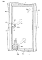
Classifications
-
- G—PHYSICS
- G09—EDUCATION; CRYPTOGRAPHY; DISPLAY; ADVERTISING; SEALS
- G09G—ARRANGEMENTS OR CIRCUITS FOR CONTROL OF INDICATING DEVICES USING STATIC MEANS TO PRESENT VARIABLE INFORMATION
- G09G3/00—Control arrangements or circuits, of interest only in connection with visual indicators other than cathode-ray tubes
- G09G3/20—Control arrangements or circuits, of interest only in connection with visual indicators other than cathode-ray tubes for presentation of an assembly of a number of characters, e.g. a page, by composing the assembly by combination of individual elements arranged in a matrix no fixed position being assigned to or needed to be assigned to the individual characters or partial characters
- G09G3/34—Control arrangements or circuits, of interest only in connection with visual indicators other than cathode-ray tubes for presentation of an assembly of a number of characters, e.g. a page, by composing the assembly by combination of individual elements arranged in a matrix no fixed position being assigned to or needed to be assigned to the individual characters or partial characters by control of light from an independent source
- G09G3/36—Control arrangements or circuits, of interest only in connection with visual indicators other than cathode-ray tubes for presentation of an assembly of a number of characters, e.g. a page, by composing the assembly by combination of individual elements arranged in a matrix no fixed position being assigned to or needed to be assigned to the individual characters or partial characters by control of light from an independent source using liquid crystals
- G09G3/3611—Control of matrices with row and column drivers
- G09G3/3648—Control of matrices with row and column drivers using an active matrix
- G09G3/3651—Control of matrices with row and column drivers using an active matrix using multistable liquid crystals, e.g. ferroelectric liquid crystals
-
- G—PHYSICS
- G02—OPTICS
- G02F—OPTICAL DEVICES OR ARRANGEMENTS FOR THE CONTROL OF LIGHT BY MODIFICATION OF THE OPTICAL PROPERTIES OF THE MEDIA OF THE ELEMENTS INVOLVED THEREIN; NON-LINEAR OPTICS; FREQUENCY-CHANGING OF LIGHT; OPTICAL LOGIC ELEMENTS; OPTICAL ANALOGUE/DIGITAL CONVERTERS
- G02F1/00—Devices or arrangements for the control of the intensity, colour, phase, polarisation or direction of light arriving from an independent light source, e.g. switching, gating or modulating; Non-linear optics
- G02F1/01—Devices or arrangements for the control of the intensity, colour, phase, polarisation or direction of light arriving from an independent light source, e.g. switching, gating or modulating; Non-linear optics for the control of the intensity, phase, polarisation or colour
- G02F1/13—Devices or arrangements for the control of the intensity, colour, phase, polarisation or direction of light arriving from an independent light source, e.g. switching, gating or modulating; Non-linear optics for the control of the intensity, phase, polarisation or colour based on liquid crystals, e.g. single liquid crystal display cells
- G02F1/133—Constructional arrangements; Operation of liquid crystal cells; Circuit arrangements
- G02F1/1333—Constructional arrangements; Manufacturing methods
- G02F1/1337—Surface-induced orientation of the liquid crystal molecules, e.g. by alignment layers
- G02F1/13378—Surface-induced orientation of the liquid crystal molecules, e.g. by alignment layers by treatment of the surface, e.g. embossing, rubbing or light irradiation
- G02F1/133784—Surface-induced orientation of the liquid crystal molecules, e.g. by alignment layers by treatment of the surface, e.g. embossing, rubbing or light irradiation by rubbing
-
- G—PHYSICS
- G02—OPTICS
- G02F—OPTICAL DEVICES OR ARRANGEMENTS FOR THE CONTROL OF LIGHT BY MODIFICATION OF THE OPTICAL PROPERTIES OF THE MEDIA OF THE ELEMENTS INVOLVED THEREIN; NON-LINEAR OPTICS; FREQUENCY-CHANGING OF LIGHT; OPTICAL LOGIC ELEMENTS; OPTICAL ANALOGUE/DIGITAL CONVERTERS
- G02F1/00—Devices or arrangements for the control of the intensity, colour, phase, polarisation or direction of light arriving from an independent light source, e.g. switching, gating or modulating; Non-linear optics
- G02F1/01—Devices or arrangements for the control of the intensity, colour, phase, polarisation or direction of light arriving from an independent light source, e.g. switching, gating or modulating; Non-linear optics for the control of the intensity, phase, polarisation or colour
- G02F1/13—Devices or arrangements for the control of the intensity, colour, phase, polarisation or direction of light arriving from an independent light source, e.g. switching, gating or modulating; Non-linear optics for the control of the intensity, phase, polarisation or colour based on liquid crystals, e.g. single liquid crystal display cells
- G02F1/133—Constructional arrangements; Operation of liquid crystal cells; Circuit arrangements
- G02F1/136—Liquid crystal cells structurally associated with a semi-conducting layer or substrate, e.g. cells forming part of an integrated circuit
- G02F1/1362—Active matrix addressed cells
-
- G—PHYSICS
- G02—OPTICS
- G02F—OPTICAL DEVICES OR ARRANGEMENTS FOR THE CONTROL OF LIGHT BY MODIFICATION OF THE OPTICAL PROPERTIES OF THE MEDIA OF THE ELEMENTS INVOLVED THEREIN; NON-LINEAR OPTICS; FREQUENCY-CHANGING OF LIGHT; OPTICAL LOGIC ELEMENTS; OPTICAL ANALOGUE/DIGITAL CONVERTERS
- G02F1/00—Devices or arrangements for the control of the intensity, colour, phase, polarisation or direction of light arriving from an independent light source, e.g. switching, gating or modulating; Non-linear optics
- G02F1/01—Devices or arrangements for the control of the intensity, colour, phase, polarisation or direction of light arriving from an independent light source, e.g. switching, gating or modulating; Non-linear optics for the control of the intensity, phase, polarisation or colour
- G02F1/13—Devices or arrangements for the control of the intensity, colour, phase, polarisation or direction of light arriving from an independent light source, e.g. switching, gating or modulating; Non-linear optics for the control of the intensity, phase, polarisation or colour based on liquid crystals, e.g. single liquid crystal display cells
- G02F1/137—Devices or arrangements for the control of the intensity, colour, phase, polarisation or direction of light arriving from an independent light source, e.g. switching, gating or modulating; Non-linear optics for the control of the intensity, phase, polarisation or colour based on liquid crystals, e.g. single liquid crystal display cells characterised by the electro-optical or magneto-optical effect, e.g. field-induced phase transition, orientation effect, guest-host interaction or dynamic scattering
- G02F1/139—Devices or arrangements for the control of the intensity, colour, phase, polarisation or direction of light arriving from an independent light source, e.g. switching, gating or modulating; Non-linear optics for the control of the intensity, phase, polarisation or colour based on liquid crystals, e.g. single liquid crystal display cells characterised by the electro-optical or magneto-optical effect, e.g. field-induced phase transition, orientation effect, guest-host interaction or dynamic scattering based on orientation effects in which the liquid crystal remains transparent
- G02F1/1393—Devices or arrangements for the control of the intensity, colour, phase, polarisation or direction of light arriving from an independent light source, e.g. switching, gating or modulating; Non-linear optics for the control of the intensity, phase, polarisation or colour based on liquid crystals, e.g. single liquid crystal display cells characterised by the electro-optical or magneto-optical effect, e.g. field-induced phase transition, orientation effect, guest-host interaction or dynamic scattering based on orientation effects in which the liquid crystal remains transparent the birefringence of the liquid crystal being electrically controlled, e.g. ECB-, DAP-, HAN-, PI-LC cells
- G02F1/1395—Optically compensated birefringence [OCB]- cells or PI- cells
-
- G—PHYSICS
- G09—EDUCATION; CRYPTOGRAPHY; DISPLAY; ADVERTISING; SEALS
- G09G—ARRANGEMENTS OR CIRCUITS FOR CONTROL OF INDICATING DEVICES USING STATIC MEANS TO PRESENT VARIABLE INFORMATION
- G09G2300/00—Aspects of the constitution of display devices
- G09G2300/04—Structural and physical details of display devices
- G09G2300/0469—Details of the physics of pixel operation
- G09G2300/0478—Details of the physics of pixel operation related to liquid crystal pixels
- G09G2300/0491—Use of a bi-refringent liquid crystal, optically controlled bi-refringence [OCB] with bend and splay states, or electrically controlled bi-refringence [ECB] for controlling the color
-
- G—PHYSICS
- G09—EDUCATION; CRYPTOGRAPHY; DISPLAY; ADVERTISING; SEALS
- G09G—ARRANGEMENTS OR CIRCUITS FOR CONTROL OF INDICATING DEVICES USING STATIC MEANS TO PRESENT VARIABLE INFORMATION
- G09G2320/00—Control of display operating conditions
- G09G2320/02—Improving the quality of display appearance
- G09G2320/0252—Improving the response speed
-
- G—PHYSICS
- G09—EDUCATION; CRYPTOGRAPHY; DISPLAY; ADVERTISING; SEALS
- G09G—ARRANGEMENTS OR CIRCUITS FOR CONTROL OF INDICATING DEVICES USING STATIC MEANS TO PRESENT VARIABLE INFORMATION
- G09G2320/00—Control of display operating conditions
- G09G2320/04—Maintaining the quality of display appearance
- G09G2320/041—Temperature compensation
-
- G—PHYSICS
- G09—EDUCATION; CRYPTOGRAPHY; DISPLAY; ADVERTISING; SEALS
- G09G—ARRANGEMENTS OR CIRCUITS FOR CONTROL OF INDICATING DEVICES USING STATIC MEANS TO PRESENT VARIABLE INFORMATION
- G09G2330/00—Aspects of power supply; Aspects of display protection and defect management
- G09G2330/02—Details of power systems and of start or stop of display operation
- G09G2330/026—Arrangements or methods related to booting a display
Landscapes
- Physics & Mathematics (AREA)
- Chemical & Material Sciences (AREA)
- Crystallography & Structural Chemistry (AREA)
- Engineering & Computer Science (AREA)
- General Physics & Mathematics (AREA)
- Nonlinear Science (AREA)
- Liquid Crystal (AREA)
- Computer Hardware Design (AREA)
- Theoretical Computer Science (AREA)
- Spectroscopy & Molecular Physics (AREA)
- Mathematical Physics (AREA)
- Optics & Photonics (AREA)
Priority Applications (2)
| Application Number | Priority Date | Filing Date | Title |
|---|---|---|---|
| JP2006146447A JP2007316387A (ja) | 2006-05-26 | 2006-05-26 | 液晶表示装置 |
| US11/753,175 US8416167B2 (en) | 2006-05-26 | 2007-05-24 | Active matrix liquid crystal display device including a transition-nucleus formation section |
Applications Claiming Priority (1)
| Application Number | Priority Date | Filing Date | Title |
|---|---|---|---|
| JP2006146447A JP2007316387A (ja) | 2006-05-26 | 2006-05-26 | 液晶表示装置 |
Publications (2)
| Publication Number | Publication Date |
|---|---|
| JP2007316387A true JP2007316387A (ja) | 2007-12-06 |
| JP2007316387A5 JP2007316387A5 (enExample) | 2008-05-29 |
Family
ID=38749067
Family Applications (1)
| Application Number | Title | Priority Date | Filing Date |
|---|---|---|---|
| JP2006146447A Pending JP2007316387A (ja) | 2006-05-26 | 2006-05-26 | 液晶表示装置 |
Country Status (2)
| Country | Link |
|---|---|
| US (1) | US8416167B2 (enExample) |
| JP (1) | JP2007316387A (enExample) |
Cited By (3)
| Publication number | Priority date | Publication date | Assignee | Title |
|---|---|---|---|---|
| WO2010001642A1 (ja) * | 2008-06-30 | 2010-01-07 | シャープ株式会社 | 液晶表示装置 |
| JP2013117680A (ja) * | 2011-12-05 | 2013-06-13 | Japan Display Central Co Ltd | 液晶表示装置および液晶表示装置の駆動方法 |
| JP2013137387A (ja) * | 2011-12-28 | 2013-07-11 | Japan Display Central Co Ltd | 液晶表示装置 |
Families Citing this family (4)
| Publication number | Priority date | Publication date | Assignee | Title |
|---|---|---|---|---|
| JP5137241B2 (ja) * | 2008-01-07 | 2013-02-06 | 株式会社ジャパンディスプレイセントラル | 液晶表示装置 |
| JP2009251489A (ja) * | 2008-04-10 | 2009-10-29 | Seiko Epson Corp | 液晶装置及び電子機器 |
| JP2014206595A (ja) * | 2013-04-11 | 2014-10-30 | 株式会社ジャパンディスプレイ | 液晶表示装置 |
| CN105892189B (zh) * | 2016-06-23 | 2019-04-02 | 京东方科技集团股份有限公司 | 阵列基板及显示装置 |
Family Cites Families (11)
| Publication number | Priority date | Publication date | Assignee | Title |
|---|---|---|---|---|
| WO2000014597A1 (en) * | 1998-09-03 | 2000-03-16 | Matsushita Electric Industrial Co., Ltd. | Liquid crystal display, method of manufacturing the same, method of driving liquid crystal display |
| JP4528455B2 (ja) | 1999-03-15 | 2010-08-18 | 東芝モバイルディスプレイ株式会社 | 液晶表示装置 |
| US6504592B1 (en) * | 1999-06-16 | 2003-01-07 | Nec Corporation | Liquid crystal display and method of manufacturing the same and method of driving the same |
| JP3971175B2 (ja) | 2000-12-19 | 2007-09-05 | 東芝松下ディスプレイテクノロジー株式会社 | 液晶表示装置およびその駆動方法 |
| WO2002050603A1 (en) * | 2000-12-19 | 2002-06-27 | Matsushita Electric Industrial Co., Ltd. | Liquid crystal display and its driving method |
| JP3334715B1 (ja) | 2001-01-25 | 2002-10-15 | 松下電器産業株式会社 | 液晶表示装置 |
| KR100498632B1 (ko) * | 2002-12-31 | 2005-07-01 | 엘지.필립스 엘시디 주식회사 | 액정 표시패널 및 그 제조방법 |
| KR100672643B1 (ko) * | 2003-12-30 | 2007-01-24 | 엘지.필립스 엘시디 주식회사 | 횡전계 방식 액정 표시 장치의 공통 전압 구동회로 |
| CN100442112C (zh) * | 2004-02-20 | 2008-12-10 | 东芝松下显示技术有限公司 | 液晶显示装置 |
| TWI285861B (en) * | 2004-05-21 | 2007-08-21 | Sanyo Electric Co | Display device |
| US7737934B2 (en) * | 2005-09-23 | 2010-06-15 | Hannstar Display Corporation | Pixel structure of liquid crystal device and driving method thereof |
-
2006
- 2006-05-26 JP JP2006146447A patent/JP2007316387A/ja active Pending
-
2007
- 2007-05-24 US US11/753,175 patent/US8416167B2/en not_active Expired - Fee Related
Cited By (5)
| Publication number | Priority date | Publication date | Assignee | Title |
|---|---|---|---|---|
| WO2010001642A1 (ja) * | 2008-06-30 | 2010-01-07 | シャープ株式会社 | 液晶表示装置 |
| US8654297B2 (en) | 2008-06-30 | 2014-02-18 | Sharp Kabushiki Kaisha | Liquid crystal display device |
| JP2013117680A (ja) * | 2011-12-05 | 2013-06-13 | Japan Display Central Co Ltd | 液晶表示装置および液晶表示装置の駆動方法 |
| US8976100B2 (en) | 2011-12-05 | 2015-03-10 | Japan Display Inc. | Liquid crystal display having a transition from splay alignment to bend alignment and driving method thereof |
| JP2013137387A (ja) * | 2011-12-28 | 2013-07-11 | Japan Display Central Co Ltd | 液晶表示装置 |
Also Published As
| Publication number | Publication date |
|---|---|
| US20070273634A1 (en) | 2007-11-29 |
| US8416167B2 (en) | 2013-04-09 |
Similar Documents
| Publication | Publication Date | Title |
|---|---|---|
| JP4989607B2 (ja) | 静電気防止回路とその製造方法及びこれを具備した液晶表示装置 | |
| CN102054454B (zh) | 液晶显示设备及其驱动方法 | |
| CN103164076B (zh) | 具有集成式触摸屏的显示装置 | |
| JP4902010B2 (ja) | 液晶装置 | |
| US20100295830A1 (en) | Electro-optical apparatus and display thereof | |
| US8416167B2 (en) | Active matrix liquid crystal display device including a transition-nucleus formation section | |
| CN102692772B (zh) | 液晶显示装置以及驱动液晶显示装置的方法 | |
| JP4559721B2 (ja) | 液晶ディスプレイの画素構造、液晶ディスプレイ駆動方法および駆動回路 | |
| JP2010002504A (ja) | 液晶表示装置 | |
| JP4579899B2 (ja) | 液晶表示装置及びその駆動方法 | |
| JP4288511B2 (ja) | Ocbモード液晶表示装置及びその駆動方法 | |
| JP4974029B2 (ja) | 液晶表示装置 | |
| JP5588958B2 (ja) | 液晶表示装置および液晶表示装置の駆動方法 | |
| JP2007316387A5 (enExample) | ||
| JP2008281702A (ja) | 液晶表示装置及び液晶表示装置の駆動方法 | |
| JP4768317B2 (ja) | 液晶表示パネル | |
| JP4891529B2 (ja) | 液晶装置 | |
| US8264439B2 (en) | Liquid crystal display panel and liquid crystal display device using the same | |
| JP2009058794A (ja) | 液晶装置、液晶装置の駆動方法、液晶装置駆動用集積回路装置および電子機器 | |
| JP5032010B2 (ja) | 液晶表示装置及びその駆動方法 | |
| KR100768196B1 (ko) | Ocb 액정표시패널의 전이구동방법 및 그 장치 | |
| JP2007156013A (ja) | 液晶表示パネル | |
| JP4675951B2 (ja) | 液晶装置の駆動方法 | |
| JP2009075215A (ja) | 液晶装置、液晶装置の駆動方法、液晶駆動用集積回路装置および電子機器 | |
| KR20040062160A (ko) | 액정 표시 장치 및 그의 구동 방법 |
Legal Events
| Date | Code | Title | Description |
|---|---|---|---|
| A521 | Written amendment |
Free format text: JAPANESE INTERMEDIATE CODE: A523 Effective date: 20080414 |
|
| A621 | Written request for application examination |
Free format text: JAPANESE INTERMEDIATE CODE: A621 Effective date: 20080414 |
|
| A977 | Report on retrieval |
Free format text: JAPANESE INTERMEDIATE CODE: A971007 Effective date: 20080708 |
|
| A131 | Notification of reasons for refusal |
Free format text: JAPANESE INTERMEDIATE CODE: A131 Effective date: 20080729 |
|
| A521 | Written amendment |
Free format text: JAPANESE INTERMEDIATE CODE: A523 Effective date: 20080925 |
|
| A02 | Decision of refusal |
Free format text: JAPANESE INTERMEDIATE CODE: A02 Effective date: 20081104 |