JP2007316387A - Liquid crystal display - Google Patents
Liquid crystal display Download PDFInfo
- Publication number
- JP2007316387A JP2007316387A JP2006146447A JP2006146447A JP2007316387A JP 2007316387 A JP2007316387 A JP 2007316387A JP 2006146447 A JP2006146447 A JP 2006146447A JP 2006146447 A JP2006146447 A JP 2006146447A JP 2007316387 A JP2007316387 A JP 2007316387A
- Authority
- JP
- Japan
- Prior art keywords
- liquid crystal
- crystal display
- display device
- pixel electrode
- pixel
- Prior art date
- Legal status (The legal status is an assumption and is not a legal conclusion. Google has not performed a legal analysis and makes no representation as to the accuracy of the status listed.)
- Pending
Links
Images


Classifications
-
- G—PHYSICS
- G09—EDUCATION; CRYPTOGRAPHY; DISPLAY; ADVERTISING; SEALS
- G09G—ARRANGEMENTS OR CIRCUITS FOR CONTROL OF INDICATING DEVICES USING STATIC MEANS TO PRESENT VARIABLE INFORMATION
- G09G3/00—Control arrangements or circuits, of interest only in connection with visual indicators other than cathode-ray tubes
- G09G3/20—Control arrangements or circuits, of interest only in connection with visual indicators other than cathode-ray tubes for presentation of an assembly of a number of characters, e.g. a page, by composing the assembly by combination of individual elements arranged in a matrix no fixed position being assigned to or needed to be assigned to the individual characters or partial characters
- G09G3/34—Control arrangements or circuits, of interest only in connection with visual indicators other than cathode-ray tubes for presentation of an assembly of a number of characters, e.g. a page, by composing the assembly by combination of individual elements arranged in a matrix no fixed position being assigned to or needed to be assigned to the individual characters or partial characters by control of light from an independent source
- G09G3/36—Control arrangements or circuits, of interest only in connection with visual indicators other than cathode-ray tubes for presentation of an assembly of a number of characters, e.g. a page, by composing the assembly by combination of individual elements arranged in a matrix no fixed position being assigned to or needed to be assigned to the individual characters or partial characters by control of light from an independent source using liquid crystals
- G09G3/3611—Control of matrices with row and column drivers
- G09G3/3648—Control of matrices with row and column drivers using an active matrix
- G09G3/3651—Control of matrices with row and column drivers using an active matrix using multistable liquid crystals, e.g. ferroelectric liquid crystals
-
- G—PHYSICS
- G02—OPTICS
- G02F—OPTICAL DEVICES OR ARRANGEMENTS FOR THE CONTROL OF LIGHT BY MODIFICATION OF THE OPTICAL PROPERTIES OF THE MEDIA OF THE ELEMENTS INVOLVED THEREIN; NON-LINEAR OPTICS; FREQUENCY-CHANGING OF LIGHT; OPTICAL LOGIC ELEMENTS; OPTICAL ANALOGUE/DIGITAL CONVERTERS
- G02F1/00—Devices or arrangements for the control of the intensity, colour, phase, polarisation or direction of light arriving from an independent light source, e.g. switching, gating or modulating; Non-linear optics
- G02F1/01—Devices or arrangements for the control of the intensity, colour, phase, polarisation or direction of light arriving from an independent light source, e.g. switching, gating or modulating; Non-linear optics for the control of the intensity, phase, polarisation or colour
- G02F1/13—Devices or arrangements for the control of the intensity, colour, phase, polarisation or direction of light arriving from an independent light source, e.g. switching, gating or modulating; Non-linear optics for the control of the intensity, phase, polarisation or colour based on liquid crystals, e.g. single liquid crystal display cells
- G02F1/133—Constructional arrangements; Operation of liquid crystal cells; Circuit arrangements
- G02F1/1333—Constructional arrangements; Manufacturing methods
- G02F1/1337—Surface-induced orientation of the liquid crystal molecules, e.g. by alignment layers
- G02F1/13378—Surface-induced orientation of the liquid crystal molecules, e.g. by alignment layers by treatment of the surface, e.g. embossing, rubbing or light irradiation
- G02F1/133784—Surface-induced orientation of the liquid crystal molecules, e.g. by alignment layers by treatment of the surface, e.g. embossing, rubbing or light irradiation by rubbing
-
- G—PHYSICS
- G02—OPTICS
- G02F—OPTICAL DEVICES OR ARRANGEMENTS FOR THE CONTROL OF LIGHT BY MODIFICATION OF THE OPTICAL PROPERTIES OF THE MEDIA OF THE ELEMENTS INVOLVED THEREIN; NON-LINEAR OPTICS; FREQUENCY-CHANGING OF LIGHT; OPTICAL LOGIC ELEMENTS; OPTICAL ANALOGUE/DIGITAL CONVERTERS
- G02F1/00—Devices or arrangements for the control of the intensity, colour, phase, polarisation or direction of light arriving from an independent light source, e.g. switching, gating or modulating; Non-linear optics
- G02F1/01—Devices or arrangements for the control of the intensity, colour, phase, polarisation or direction of light arriving from an independent light source, e.g. switching, gating or modulating; Non-linear optics for the control of the intensity, phase, polarisation or colour
- G02F1/13—Devices or arrangements for the control of the intensity, colour, phase, polarisation or direction of light arriving from an independent light source, e.g. switching, gating or modulating; Non-linear optics for the control of the intensity, phase, polarisation or colour based on liquid crystals, e.g. single liquid crystal display cells
- G02F1/133—Constructional arrangements; Operation of liquid crystal cells; Circuit arrangements
- G02F1/136—Liquid crystal cells structurally associated with a semi-conducting layer or substrate, e.g. cells forming part of an integrated circuit
- G02F1/1362—Active matrix addressed cells
-
- G—PHYSICS
- G02—OPTICS
- G02F—OPTICAL DEVICES OR ARRANGEMENTS FOR THE CONTROL OF LIGHT BY MODIFICATION OF THE OPTICAL PROPERTIES OF THE MEDIA OF THE ELEMENTS INVOLVED THEREIN; NON-LINEAR OPTICS; FREQUENCY-CHANGING OF LIGHT; OPTICAL LOGIC ELEMENTS; OPTICAL ANALOGUE/DIGITAL CONVERTERS
- G02F1/00—Devices or arrangements for the control of the intensity, colour, phase, polarisation or direction of light arriving from an independent light source, e.g. switching, gating or modulating; Non-linear optics
- G02F1/01—Devices or arrangements for the control of the intensity, colour, phase, polarisation or direction of light arriving from an independent light source, e.g. switching, gating or modulating; Non-linear optics for the control of the intensity, phase, polarisation or colour
- G02F1/13—Devices or arrangements for the control of the intensity, colour, phase, polarisation or direction of light arriving from an independent light source, e.g. switching, gating or modulating; Non-linear optics for the control of the intensity, phase, polarisation or colour based on liquid crystals, e.g. single liquid crystal display cells
- G02F1/137—Devices or arrangements for the control of the intensity, colour, phase, polarisation or direction of light arriving from an independent light source, e.g. switching, gating or modulating; Non-linear optics for the control of the intensity, phase, polarisation or colour based on liquid crystals, e.g. single liquid crystal display cells characterised by the electro-optical or magneto-optical effect, e.g. field-induced phase transition, orientation effect, guest-host interaction or dynamic scattering
- G02F1/139—Devices or arrangements for the control of the intensity, colour, phase, polarisation or direction of light arriving from an independent light source, e.g. switching, gating or modulating; Non-linear optics for the control of the intensity, phase, polarisation or colour based on liquid crystals, e.g. single liquid crystal display cells characterised by the electro-optical or magneto-optical effect, e.g. field-induced phase transition, orientation effect, guest-host interaction or dynamic scattering based on orientation effects in which the liquid crystal remains transparent
- G02F1/1393—Devices or arrangements for the control of the intensity, colour, phase, polarisation or direction of light arriving from an independent light source, e.g. switching, gating or modulating; Non-linear optics for the control of the intensity, phase, polarisation or colour based on liquid crystals, e.g. single liquid crystal display cells characterised by the electro-optical or magneto-optical effect, e.g. field-induced phase transition, orientation effect, guest-host interaction or dynamic scattering based on orientation effects in which the liquid crystal remains transparent the birefringence of the liquid crystal being electrically controlled, e.g. ECB-, DAP-, HAN-, PI-LC cells
- G02F1/1395—Optically compensated birefringence [OCB]- cells or PI- cells
-
- G—PHYSICS
- G09—EDUCATION; CRYPTOGRAPHY; DISPLAY; ADVERTISING; SEALS
- G09G—ARRANGEMENTS OR CIRCUITS FOR CONTROL OF INDICATING DEVICES USING STATIC MEANS TO PRESENT VARIABLE INFORMATION
- G09G2300/00—Aspects of the constitution of display devices
- G09G2300/04—Structural and physical details of display devices
- G09G2300/0469—Details of the physics of pixel operation
- G09G2300/0478—Details of the physics of pixel operation related to liquid crystal pixels
- G09G2300/0491—Use of a bi-refringent liquid crystal, optically controlled bi-refringence [OCB] with bend and splay states, or electrically controlled bi-refringence [ECB] for controlling the color
-
- G—PHYSICS
- G09—EDUCATION; CRYPTOGRAPHY; DISPLAY; ADVERTISING; SEALS
- G09G—ARRANGEMENTS OR CIRCUITS FOR CONTROL OF INDICATING DEVICES USING STATIC MEANS TO PRESENT VARIABLE INFORMATION
- G09G2320/00—Control of display operating conditions
- G09G2320/02—Improving the quality of display appearance
- G09G2320/0252—Improving the response speed
-
- G—PHYSICS
- G09—EDUCATION; CRYPTOGRAPHY; DISPLAY; ADVERTISING; SEALS
- G09G—ARRANGEMENTS OR CIRCUITS FOR CONTROL OF INDICATING DEVICES USING STATIC MEANS TO PRESENT VARIABLE INFORMATION
- G09G2320/00—Control of display operating conditions
- G09G2320/04—Maintaining the quality of display appearance
- G09G2320/041—Temperature compensation
-
- G—PHYSICS
- G09—EDUCATION; CRYPTOGRAPHY; DISPLAY; ADVERTISING; SEALS
- G09G—ARRANGEMENTS OR CIRCUITS FOR CONTROL OF INDICATING DEVICES USING STATIC MEANS TO PRESENT VARIABLE INFORMATION
- G09G2330/00—Aspects of power supply; Aspects of display protection and defect management
- G09G2330/02—Details of power systems and of start or stop of display operation
- G09G2330/026—Arrangements or methods related to booting a display
Abstract
Description
この発明は、液晶表示装置に関し、特に、アクティブマトリクス型の液晶表示装置に関する。 The present invention relates to a liquid crystal display device, and more particularly to an active matrix type liquid crystal display device.
一般に液晶表示装置は、マトリクス状に配置された表示画素からなる表示部を有する液晶表示パネルを備えている。この液晶表示パネルは、互いに対向する一対の基板、すなわち、アレイ基板および対向基板と、一対の基板間に挟持された液晶層とを有している。 In general, a liquid crystal display device includes a liquid crystal display panel having a display unit composed of display pixels arranged in a matrix. This liquid crystal display panel has a pair of substrates facing each other, that is, an array substrate and a counter substrate, and a liquid crystal layer sandwiched between the pair of substrates.
アレイ基板は、前記複数の表示画素のそれぞれに対応して配置された画素電極を有し、対向基板は複数の画素電極に対向する対向電極を有している。 The array substrate has pixel electrodes arranged corresponding to the plurality of display pixels, and the counter substrate has counter electrodes facing the pixel electrodes.
OCB(Optically Compensated Bend)モードによる液晶表示装置は、TNモード等の液晶表示装置に較べて、高速応答・高視野角であるという特徴を有する。このことから、OCBモードの液晶表示装置は、例えば、今後の市場拡大が期待されている液晶テレビ製品向けとして適当である。 A liquid crystal display device using an OCB (Optically Compensated Bend) mode is characterized by a high-speed response and a high viewing angle compared to a liquid crystal display device such as a TN mode. Accordingly, the OCB mode liquid crystal display device is suitable for, for example, a liquid crystal television product for which future market expansion is expected.
このOCBモードの液晶表示装置では、液晶層に電圧が印加されていないときには、液晶層に含まれる液晶分子の配向状態が非表示状態であるスプレイ配向となっているため、OCBモードの液晶表示装置を起動する際には、非表示状態での液晶分子の配向状態から、表示状態での液晶分子の配向状態(ベンド配向)へ配向状態を変化(以下、転移という)させて初期化する必要がある。 In this OCB mode liquid crystal display device, when no voltage is applied to the liquid crystal layer, the alignment state of the liquid crystal molecules contained in the liquid crystal layer is a splay alignment which is a non-display state. , It is necessary to initialize by changing the alignment state (hereinafter referred to as transition) from the alignment state of the liquid crystal molecules in the non-display state to the alignment state (bend alignment) of the liquid crystal molecules in the display state. is there.
従来、隣合う画素電極間で横電界を生じさせて、画像を表示させる前に液晶分子の配向状態を非表示状態の配向状態から表示状態の配向状態への転移を促進し、これにより速やかに画像を表示させる液晶表示装置が提案されている(特許文献1参照)。
しかし、転移の際には、液晶分子の配向状態は画素電極および対向電極上に配置された配向膜のラビング方向と逆方向に最も早く転移が進むが、上記の液晶表示装置では、配向膜のラビング方向が考慮されておらず、転移が開始される位置によっては、転移が開始されてから初期化が完了するまで時間を要する場合があり、画素サイズが大きいパネルにおいては、初期化が完了するまでの時間をさらに要する場合があった。 However, at the time of transition, the alignment state of the liquid crystal molecules proceeds most rapidly in the direction opposite to the rubbing direction of the alignment film disposed on the pixel electrode and the counter electrode. The rubbing direction is not taken into account, and depending on the position where the transition is started, it may take time from the start of the transition to the completion of initialization. In a panel with a large pixel size, the initialization is completed. In some cases, more time was required.
また、特に、低温環境においては液晶材料の粘性が増し、初期化に必要な時間がさらに増大する場合があった。 In particular, the viscosity of the liquid crystal material increases in a low temperature environment, and the time required for initialization may further increase.
本発明は、上記の問題点に鑑みて成されたものであって、OCBモードの液晶表示装置において、初期化に要する時間を短縮することを目的とする。 The present invention has been made in view of the above problems, and an object of the present invention is to shorten the time required for initialization in an OCB mode liquid crystal display device.
本発明の態様による液晶表示装置は、第1基板と第2基板との間に挟持された液晶層を備え、マトリクス状に配置された複数の表示画素からなる表示部を有するOCBモードの液晶表示装置であって、前記第1基板は、前記複数の表示画素のそれぞれに対応して配置された画素電極を有し、前記第2基板は、前記複数の画素電極に対向する対向電極を有し、前記第1基板および前記第2基板は、前記画素電極および前記対向電極上にそれぞれ配置されているとともに、ラビング処理によって前記液晶層に含まれる液晶分子の配向状態を制御する一対の配向膜、を備え、各表示画素において、前記配向膜のラビング方向の終端側に、前記液晶層に含まれる液晶分子の配向状態を非表示状態から表示状態へ転移させるための電界を形成する転移形成部が設けられている。 A liquid crystal display device according to an aspect of the present invention includes an OCB mode liquid crystal display including a liquid crystal layer sandwiched between a first substrate and a second substrate, and having a display unit including a plurality of display pixels arranged in a matrix. In the apparatus, the first substrate has pixel electrodes arranged corresponding to the plurality of display pixels, and the second substrate has counter electrodes facing the plurality of pixel electrodes. The first substrate and the second substrate are disposed on the pixel electrode and the counter electrode, respectively, and a pair of alignment films for controlling the alignment state of the liquid crystal molecules contained in the liquid crystal layer by rubbing treatment, In each display pixel, a transition type that forms an electric field for transitioning the alignment state of liquid crystal molecules contained in the liquid crystal layer from a non-display state to a display state on the end side in the rubbing direction of the alignment film Part is provided.
この発明によれば、OCBモードの液晶表示装置において、初期化に要する時間を短縮する液晶表示装置を提供することができる。 According to the present invention, in the OCB mode liquid crystal display device, it is possible to provide a liquid crystal display device that shortens the time required for initialization.
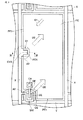
以下、本発明の第1実施形態に係る液晶表示装置について図面を参照して説明する。本実施形態に係る液晶表示装置は、図1に示すように、略矩形平板状の液晶表示パネル10を備えている。液晶表示パネル10は、互いに対向する一対の基板、すなわちアレイ基板12および対向基板14を有している。アレイ基板12と対向基板14との間には液晶層LQが挟持されている。
Hereinafter, a liquid crystal display device according to a first embodiment of the present invention will be described with reference to the drawings. As shown in FIG. 1, the liquid crystal display device according to the present embodiment includes a liquid
液晶表示パネル10は、マトリクス状に配置された複数の表示画素PXからなる表示部10Aと、表示部10Aの周囲の周辺部10Bとを有している。
The liquid
表示部10Aには、複数の表示画素PXが配置された行に沿って複数の走査線Y(Y1〜Ym)が配置され、複数の表示画素PXが配置された列に沿って複数の信号線X(X1〜Xn)が配置されている。複数の走査線Yは、周辺部10Bに配置された走査線駆動回路GDに接続されている。複数の信号線Xは、周辺部10Bに配置された信号線駆動回路SDに接続されている。
In the
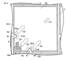
各表示画素PXは、アレイ基板12上に、例えば薄膜トランジスタ(TFT:Thin Film Transistor)からなる画素スイッチSWを有している。画素スイッチSWのゲート電極GEは、図2に示すように、対応する走査線Yに接続されている(あるいは一体に形成されている)。画素スイッチSWのソース電極SEは、対応する信号線Xに接続されている(あるいは一体に形成されている)。画素スイッチSWのドレイン電極DEは、アレイ基板12上において、各表示画素PXに配置された画素電極PEにコンタクトホールCHによって接続されている。
Each display pixel PX has a pixel switch SW made of, for example, a thin film transistor (TFT) on the
本実施形態において、画素電極PEは略矩形状であって、対向基板14上に配置された対向電極CEに対向するように配置されている。画素電極PEおよび対向電極CE上には、ラビング処理によって液晶層LQに含まれる液晶分子の配向状態を制御する一対の配向膜(図示せず)が配置されている。本実施形態に係る液晶表示装置では、配向膜は図2に示すD1方向にラビングされている。
In the present embodiment, the pixel electrode PE has a substantially rectangular shape, and is disposed so as to face the counter electrode CE disposed on the
図2に示すように、各表示画素には、配向膜のラビング方向D1の終端側に、液晶層LQに含まれる液晶分子の配向状態を転移させるための転移核A2を形成する転移形成部A1が設けられている。本実施形態の場合、転移形成部A1は、矩形状の表示画素PXの長辺側に設けられている。 As shown in FIG. 2, in each display pixel, a transition formation portion A1 that forms a transition nucleus A2 for transitioning the alignment state of the liquid crystal molecules contained in the liquid crystal layer LQ on the end side of the alignment film in the rubbing direction D1. Is provided. In the present embodiment, the transition formation portion A1 is provided on the long side of the rectangular display pixel PX.
転移形成部A1は、画素電極PEの凹部PEAと、画素電極PEとは異なる電位となる配線、すなわち信号線Xとによって構成されている。すなわち、図2および図4に示すように、転移形成部A1において、画素電極PEは、ラビング方向D1の終端側の端辺PE1に略矩形状の凹部PEAを有している。信号線Xは、画素電極PEの端辺PE1側に延びた凸部CVXを有し、画素電極PE1の凹部PEAと信号線Xの凸部CVXとは絶縁層を介して少なくとも一部で対向するように配置されている。 The transition formation portion A1 includes a recess PEA of the pixel electrode PE and a wiring having a different potential from the pixel electrode PE, that is, a signal line X. That is, as shown in FIGS. 2 and 4, in the transition formation portion A1, the pixel electrode PE has a substantially rectangular recess PEA on the end side PE1 on the terminal side in the rubbing direction D1. The signal line X has a convex portion CVX extending toward the end PE1 of the pixel electrode PE, and the concave portion PEA of the pixel electrode PE1 and the convex portion CVX of the signal line X are at least partially opposed via an insulating layer. Are arranged as follows.
ここで、ラビング方向D1の終端側の端辺PE1とは、図3に示すように、核表示画素において、画素電極PEの端辺のうち、ラビング方向D1と2回目以降に交差する端辺である。すなわち、本実施形態の場合は、ラビング方向D1の終端側の端辺PE1は、画素スイッチSWに隣接する端辺となる。すなわち、本実施形態では、画素電極PEの凹部PEAは、画素電極PEの長辺であってラビング方向D1の終端側の端辺PE1に配置されている。 Here, the edge PE1 on the terminal side in the rubbing direction D1 is an edge that intersects the rubbing direction D1 for the second and subsequent times among the edges of the pixel electrode PE in the core display pixel, as shown in FIG. is there. That is, in the present embodiment, the end side PE1 on the terminal side in the rubbing direction D1 is an end side adjacent to the pixel switch SW. In other words, in the present embodiment, the concave portion PEA of the pixel electrode PE is arranged on the long side of the pixel electrode PE and on the end side PE1 on the terminal side in the rubbing direction D1.
上記のように、画素電極PEの凹部PEAと信号線Xの凸部CVXとを配置すると、画素電極PEと信号線Xとに異なる電位となったときに、図5に示すように、画素電極PEの凹部PEAと信号線Xの凸部CVXとの間に電界が発生する。この電界は、画素電極PEの面方向と略平行な平面上で凹部PEAの端辺と略直交する方向に発生する。すなわち、画素電極PEと対向電極CEとの間に発生する電界は異なる平面上に電界が発生することになる。本実施形態の場合、凹部PEAの端辺に沿って180°の範囲に電界が発生する。 As described above, when the concave portion PEA of the pixel electrode PE and the convex portion CVX of the signal line X are arranged, when the pixel electrode PE and the signal line X have different potentials, as shown in FIG. An electric field is generated between the concave portion PEA of the PE and the convex portion CVX of the signal line X. This electric field is generated in a direction substantially orthogonal to the edge of the recess PEA on a plane substantially parallel to the surface direction of the pixel electrode PE. That is, the electric field generated between the pixel electrode PE and the counter electrode CE is generated on a different plane. In the case of the present embodiment, an electric field is generated in the range of 180 ° along the edge of the recess PEA.
液晶層LQ内に電界が発生すると、この電界近傍にある液晶分子は電界の方向に配列する。そうすると、本実施形態の様に、凹部PEAの端辺にそって180°の範囲に凹部PEAの端辺に対して略直交する方向に電界が発生する場合には、局所的に、画素電極PEと対向電極CEとの間に発生する電界とは異なる方向の電界が発生する事になる。このような領域は液晶分子の配向状態の変化が生じやすくなる。 When an electric field is generated in the liquid crystal layer LQ, liquid crystal molecules in the vicinity of the electric field are aligned in the direction of the electric field. Then, as in the present embodiment, when an electric field is generated in a direction substantially orthogonal to the end side of the recess PEA in the range of 180 ° along the end side of the recess PEA, the pixel electrode PE is locally generated. An electric field in a direction different from the electric field generated between the counter electrode CE and the counter electrode CE is generated. In such a region, the alignment state of the liquid crystal molecules easily changes.
従って、転移形成部A1によって、初期化する際に液晶分子の配向状態を図6に示すように非表示状態(スプレイ配向)から表示状態(ベンド配向)へ変化させるための転移核A2が形成されることになる。 Accordingly, the transition formation portion A1 forms a transition nucleus A2 for changing the alignment state of the liquid crystal molecules from the non-display state (splay alignment) to the display state (bend alignment) as shown in FIG. Will be.
また、図2に示す場合では、画素スイッチSWが配置された領域も同様に、画素電極PEと画素スイッチSWとの間に電界が生じ、転移核A2となる。したがって、本実施形態の場合には、画素電極PEの凹部PEAと信号線Xの凸部が重なる位置、すなわち転移形成部A1と画素スイッチSWとの2箇所に転移核A2が形成され、これらの転移核A2によって、初期化の際に液晶分子の転移が促されることになる。 In the case shown in FIG. 2, an electric field is similarly generated between the pixel electrode PE and the pixel switch SW in the region where the pixel switch SW is arranged, and becomes a transition nucleus A2. Therefore, in the case of the present embodiment, transition nuclei A2 are formed at two positions where the concave portion PEA of the pixel electrode PE and the convex portion of the signal line X overlap, that is, the transition formation portion A1 and the pixel switch SW. The transition nucleus A2 promotes the transition of liquid crystal molecules during initialization.
ここで、図7に示すように、表示画素PXに転移核A2が発生した場合、各表示画素PXにおいて転移が進む速さはラビング方向D1に対して逆の方向に最も速くなる。すなわち、ラビング方向D1に対して逆方向であるD2方向に進む速さが最も早くなる。 Here, as shown in FIG. 7, when the transition nucleus A2 is generated in the display pixel PX, the speed at which the transition proceeds in each display pixel PX is fastest in the direction opposite to the rubbing direction D1. That is, the speed of traveling in the direction D2 that is the opposite direction to the rubbing direction D1 is the fastest.
このことから、各表示画素PXにおいて、上記の様に転移核A2をラビング方向D1の終端側に形成することによって、転移が進む方向D2が表示画素PXを横断する方向とになり、液晶分子の配向状態の転移が迅速に進むことになる。 From this, in each display pixel PX, by forming the transition nucleus A2 on the terminal side in the rubbing direction D1 as described above, the direction D2 in which the transition proceeds becomes the direction crossing the display pixel PX, and the liquid crystal molecules The transition of the alignment state proceeds rapidly.
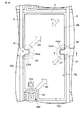
さらに、図1に示すように、本実施形態に係る液晶表示装置は、信号線駆動回路SD及び走査線駆動回路GD等を制御するコントローラCTR、および、液晶表示装置の外部の温度を測定するためのセンサSをさらに有している。コントローラCTRは、液晶表示装置が起動する際に、センサSからの測定結果によって液晶層LQに印加される電圧を制御する初期制御部CIを有している。 Further, as shown in FIG. 1, the liquid crystal display device according to the present embodiment measures the temperature outside the liquid crystal display device, and the controller CTR that controls the signal line drive circuit SD, the scanning line drive circuit GD, and the like. The sensor S is further provided. The controller CTR has an initial control unit CI that controls the voltage applied to the liquid crystal layer LQ according to the measurement result from the sensor S when the liquid crystal display device is activated.
コントローラCTRは走査線駆動回路GDを制御して、タイミング信号YTに合わせて走査線Yを選択させる。すなわち、走査線Yは走査線駆動回路GDからの走査信号Vgによって順次選択される。走査線Yが選択されると、選択された走査線Yに接続された画素スイッチSWが導通する。コントローラCTRは信号線駆動回路SDを制御して、タイミング信号XTに合わせて信号線Xに画像データVsを送信させる。信号線駆動回路SDから信号線Xに出力された画像データVsは、画素スイッチSWを介して画素電極PEに印加される。 The controller CTR controls the scanning line driving circuit GD to select the scanning line Y in accordance with the timing signal YT. That is, the scanning lines Y are sequentially selected by the scanning signal Vg from the scanning line driving circuit GD. When the scanning line Y is selected, the pixel switch SW connected to the selected scanning line Y becomes conductive. The controller CTR controls the signal line driving circuit SD to transmit the image data Vs to the signal line X in accordance with the timing signal XT. The image data Vs output from the signal line drive circuit SD to the signal line X is applied to the pixel electrode PE via the pixel switch SW.
コントローラCTRの初期制御部CIは、液晶表示装置の初期化の際に、図8に示すように、走査信号Vg、画像データVs、および、コモン信号Vcomを液晶表示パネル10に送信する。このときに、コントローラCTRの初期制御部CIは、センサSに外部の温度を測定させて、センサSの測定結果によって液晶表示パネル10に送信するコモン信号Vcomの大きさを制御する。
When the liquid crystal display device is initialized, the initial control unit CI of the controller CTR transmits the scanning signal Vg, the image data Vs, and the common signal Vcom to the liquid
すなわち、外部の温度が低くなると液晶材料の粘性が増し液晶分子の配列状態の変化が抑制される。そのため、初期制御部CIは、センサSの測定結果がある一定の温度よりも低い場合には、画像データVsの中央値Vscに対してコモン信号Vcomを大きく設定する。すなわち、|Vcom−Vsc|の値を大きくする。 That is, when the external temperature decreases, the viscosity of the liquid crystal material increases and the change in the alignment state of the liquid crystal molecules is suppressed. Therefore, when the measurement result of the sensor S is lower than a certain temperature, the initial control unit CI sets the common signal Vcom larger than the median value Vsc of the image data Vs. That is, the value of | Vcom−Vsc | is increased.
そうすると、液晶材料の粘性が高い場合には、画素電極PEと対向電極CEとの間に挟持された液晶層LQに印加される電圧が高くなる、すなわち、液晶分子の配列状態を非表示状態から表示状態へと変化させるための電圧が大きくなるため、液晶分子の転移に要する時間が短縮されることになる。 Then, when the viscosity of the liquid crystal material is high, the voltage applied to the liquid crystal layer LQ sandwiched between the pixel electrode PE and the counter electrode CE increases, that is, the alignment state of the liquid crystal molecules is changed from the non-display state. Since the voltage for changing to the display state increases, the time required for the transition of the liquid crystal molecules is shortened.
したがって、本実施形態に係る液晶表示装置によれば、OCBモードの液晶表示装置において初期化に要する時間を短縮することができ、特に、低温環境下であっても初期転移時間を短縮することができる液晶表示装置を提供できる。 Therefore, according to the liquid crystal display device according to the present embodiment, the time required for initialization in the OCB mode liquid crystal display device can be shortened, and in particular, the initial transition time can be shortened even in a low temperature environment. A liquid crystal display device can be provided.
次に、本発明の第2実施形態に係る液晶表示装置について図面を参照して説明する。なお、以下の説明において、第1実施形態に係る液晶表示装置と同様の構成については同一の符号を付して説明を省略する。 Next, a liquid crystal display device according to a second embodiment of the present invention will be described with reference to the drawings. In the following description, the same components as those of the liquid crystal display device according to the first embodiment are denoted by the same reference numerals and description thereof is omitted.
本実施形態に係る液晶表示装置は、前述の第1実施形態に係る液晶表示装置と同様に、各表示画素PXにおいてラビング方向D1の終端側に転移形成部A1を有している。すなわち、本実施形態に係る液晶表示装置では、転移形成部A1は、ラビング方向D1の終端側の端辺PE1であって、矩形状の表示画素PXの短辺側に設けられている。 Similarly to the liquid crystal display device according to the first embodiment, the liquid crystal display device according to the present embodiment has the transition formation portion A1 on the terminal side in the rubbing direction D1 in each display pixel PX. That is, in the liquid crystal display device according to the present embodiment, the transition formation portion A1 is provided on the end side PE1 on the terminal end side in the rubbing direction D1 and on the short side of the rectangular display pixel PX.
転移形成部A1は、画素電極PEの凹部PEAと、絶縁層を介して凹部PEAと一部において対向するとともに画素電極PEとは異なる電位となる配線、すなわち走査線Yとによって構成されている。画素電極PEの凹部PEAは、走査線Yと絶縁層を介して少なくともその一部が対向するように配置されている。 The transition formation portion A1 includes a recess PEA of the pixel electrode PE and a wiring that partially faces the recess PEA via an insulating layer and has a potential different from that of the pixel electrode PE, that is, a scanning line Y. The recess PEA of the pixel electrode PE is arranged so that at least a part thereof faces the scanning line Y with the insulating layer interposed therebetween.
すなわち、画素電極PEは、短辺であってラビング方向D1の終端側の端辺PE1に凹部PEAを有している。走査線Yは、図9および図10に示すように、画素電極PEの端辺PE1側に延びた凸部CVXを有している。画素電極PE1の凹部PEAと走査線Yの凸部CVXとは、絶縁層を介して少なくとも一部で対向するように配置されている。 That is, the pixel electrode PE has a concave portion PEA on the end side PE1 which is a short side and is on the terminal side in the rubbing direction D1. As shown in FIGS. 9 and 10, the scanning line Y has a convex portion CVX extending toward the end PE1 of the pixel electrode PE. The concave part PEA of the pixel electrode PE1 and the convex part CVX of the scanning line Y are arranged so as to be opposed at least partially via the insulating layer.
上記のように、転移形成部A1において画素電極PEの凹部PEAと走査線Yの凸部CVXとを配置すると、図5に示す場合と同様に、画素電極PEの凹部PEAの端辺に略直交する方向に電界が発生する。そうすると、画素電極PEの凹部PEAと走査線Yの凸部CVXとが重なる位置、すなわち転移形成部A1に転移核A2が形成されることになる。初期化の際には、この転移核A2によって転移が促される。 As described above, when the concave portion PEA of the pixel electrode PE and the convex portion CVX of the scanning line Y are arranged in the transition formation portion A1, as in the case shown in FIG. 5, it is substantially orthogonal to the edge of the concave portion PEA of the pixel electrode PE. An electric field is generated in the direction of Then, the transition nucleus A2 is formed at the position where the concave portion PEA of the pixel electrode PE and the convex portion CVX of the scanning line Y overlap, that is, the transition formation portion A1. At the time of initialization, the transition is promoted by the transition nucleus A2.
このとき、前述の第1実施形態の場合と同様に、転移が進む速さはラビング方向D1に対して逆方向D2に最も速くなる。従って、上記の様に各表示画素PXにおいてラビング方向D1の終端側に転移形成部A1を有することによって、初期化に要する時間を短縮することができる。 At this time, as in the case of the first embodiment described above, the speed at which the transition proceeds is the fastest in the reverse direction D2 with respect to the rubbing direction D1. Therefore, the time required for initialization can be shortened by having the transition formation portion A1 on the terminal side in the rubbing direction D1 in each display pixel PX as described above.
従って、本実施形態に係る液晶表示装置によれば、OCBモードの液晶表示装置において初期化に要する時間を短縮することができる。また、第1実施形態と同様にコントローラCTRが初期制御部CIを備える場合には、低温環境下であっても初期転移時間を短縮することができる液晶表示装置を提供できる。 Therefore, according to the liquid crystal display device according to the present embodiment, it is possible to reduce the time required for initialization in the OCB mode liquid crystal display device. Further, as in the first embodiment, when the controller CTR includes the initial control unit CI, it is possible to provide a liquid crystal display device that can shorten the initial transition time even in a low temperature environment.
次に、本発明の第3実施形態について図面を参照して説明する。 Next, a third embodiment of the present invention will be described with reference to the drawings.
本実施形態に係る液晶表示装置は、前述の第1実施形態に係る液晶表示装置と同様に、各表示画素においてラビング方向D1の終端側に転移形成部A1を有している。すなわち、本実施形態に係る液晶表示装置は、各表示画素PXにおいて、配向膜のラビング方向D1の終端側の端辺PE1である長辺側に転移形成部A1を有している。 Similarly to the liquid crystal display device according to the first embodiment described above, the liquid crystal display device according to the present embodiment has the transition formation portion A1 on the terminal side in the rubbing direction D1 in each display pixel. In other words, the liquid crystal display device according to the present embodiment has the transition formation portion A1 on the long side which is the end side PE1 on the end side in the rubbing direction D1 of the alignment film in each display pixel PX.
転移形成部A1は、画素電極PEの凹部PEAと、絶縁膜を介して凹部PEAと一部において対向するとともに画素電極PEとは異なる電位となる配線、すなわち補助容量線Csとによって構成されている。すなわち、図11に示すように、本実施形態に係る液晶表示装置の液晶表示パネル10は、表示部10Aにおいて走査線Yと略平行に延びる補助容量線Csを有している。補助容量線Csは画素電極PEを横断するように配置されている。
The transition formation portion A1 is configured by a recess PEA of the pixel electrode PE and a wiring that partially opposes the recess PEA via an insulating film and has a different potential from the pixel electrode PE, that is, an auxiliary capacitance line Cs. . That is, as shown in FIG. 11, the liquid
画素電極PEは、前述の第1実施形態の場合と同様に、配向膜のラビング方向D1の終端側の端辺PE1に凹部PEAを有している。凹部PEAは、補助容量線Csが配置されている位置に形成されている。すなわち、図12に示すように、補助容量線Cs上には絶縁膜が配置され、画素電極PE1の凹部PEAと補助容量線Csとは、この絶縁層を介して対向するように配置されている。 As in the case of the first embodiment described above, the pixel electrode PE has a recess PEA on the end side PE1 on the end side in the rubbing direction D1 of the alignment film. The recess PEA is formed at a position where the auxiliary capacitance line Cs is disposed. That is, as shown in FIG. 12, an insulating film is arranged on the auxiliary capacitance line Cs, and the concave portion PEA of the pixel electrode PE1 and the auxiliary capacitance line Cs are arranged so as to face each other through this insulating layer. .
上記の様に、補助容量線Csと画素電極PEの凹部PEAとを配置すると、図5に示す信号線Xと画素電極PEとの間と同様に、補助容量線Csと画素電極PEの凹部PEAとの間で、凹部PEAの端辺に対して略直交する方向に電界が発生する。そうすると、画素電極PEの凹部PEAと補助容量線Csとが重なる位置、すなわち転移形成部A1に、転移核A2が形成される。初期化の際にはこの転移核A2において転移が促される。 As described above, when the auxiliary capacitance line Cs and the concave portion PEA of the pixel electrode PE are arranged, the auxiliary capacitance line Cs and the concave portion PEA of the pixel electrode PE are disposed as between the signal line X and the pixel electrode PE shown in FIG. An electric field is generated in a direction substantially perpendicular to the edge of the recess PEA. As a result, the transition nucleus A2 is formed at the position where the concave portion PEA of the pixel electrode PE and the auxiliary capacitance line Cs overlap, that is, at the transition formation portion A1. At the time of initialization, the transition is promoted in the transition nucleus A2.
このとき、前述の第1実施形態の場合と同様に、転移が進む速さはラビング方向D1に対して逆方向D2に最も速くなる。従って、上記の様に各表示画素PXにおいてラビング方向D1の終端側に転移形成部A1を有することによって、初期化に要する時間を短縮することができる。 At this time, as in the case of the first embodiment described above, the speed at which the transition proceeds is the fastest in the reverse direction D2 with respect to the rubbing direction D1. Therefore, the time required for initialization can be shortened by having the transition formation portion A1 on the terminal side in the rubbing direction D1 in each display pixel PX as described above.
すなわち、本実施形態に係る液晶表示装置によれば、前述の第1実施形態の場合と同様に、OCBモードの液晶表示装置において初期化に要する時間を短縮することができる。また、第1実施形態と同様にコントローラCTRが初期制御部CIを備える場合には、低温環境下であっても初期転移時間を短縮することができる液晶表示装置を提供できる。 That is, according to the liquid crystal display device according to the present embodiment, the time required for initialization in the OCB mode liquid crystal display device can be shortened as in the case of the first embodiment described above. Further, as in the first embodiment, when the controller CTR includes the initial control unit CI, it is possible to provide a liquid crystal display device that can shorten the initial transition time even in a low temperature environment.
次に、本発明の第4実施形態に係る液晶表示装置について図面を参照して説明する。本実施形態に係る液晶表示装置は、前述の第1実施形態の場合と同様に、各表示画素PXにおいてラビング方向の終端側に転移形成部A1を有している。本実施形態に係る液晶表示装置は、各表示画素PXにおいて、画素電極PEのラビング方向D1の終端側の端辺PE1である長辺側と、ラビング方向D1の始端側の端辺である長辺側とに転移形成部A1を有している。 Next, a liquid crystal display device according to a fourth embodiment of the present invention is described with reference to the drawings. The liquid crystal display device according to the present embodiment has the transition formation portion A1 on the end side in the rubbing direction in each display pixel PX, as in the case of the first embodiment described above. In the liquid crystal display device according to the present embodiment, in each display pixel PX, the long side that is the end side PE1 of the pixel electrode PE in the rubbing direction D1 and the long side that is the end side of the starting end side in the rubbing direction D1. It has a transition formation portion A1 on the side.
転移形成部A1は、画素電極PEの凹部PEAと画素電極PEとは異なる電位となる配線、すなわち補助容量線Csとによって構成されている。すなわち、図13に示すように、表示部10Aにおいて走査線Yに対して略平行に延びる補助容量線Csを有している。補助容量線Csは、表示画素PXが配列する行に沿って配置された分岐部CsAを有している。すなわち、分岐部CsAは、図13に示すように、信号線Xに沿って延びている。分岐部CsAは、画素電極PE側に突出した凸部CVXを有している。
The transition formation portion A1 is constituted by a wiring having a different potential between the concave portion PEA of the pixel electrode PE and the pixel electrode PE, that is, an auxiliary capacitance line Cs. That is, as shown in FIG. 13, the
画素電極PEは、補助容量線Csの分岐部CsAの凸部CVXおよびとその一部が対向する凹部PEAを有している。凹部PEAは、少なくとも画素電極PEのラビング方向D1の終端側の端辺PE1に形成されている。本実施形態の場合、凹部PEAは画素電極PEの2つの長辺に形成されている。 The pixel electrode PE has a convex portion CVX of the branching portion CsA of the auxiliary capacitance line Cs and a concave portion PEA partially opposed to the convex portion CVX. The recess PEA is formed at least on the end PE1 on the terminal end side in the rubbing direction D1 of the pixel electrode PE. In the present embodiment, the recess PEA is formed on two long sides of the pixel electrode PE.
図14に示すように、補助容量線Cs上に絶縁膜が配置され、この絶縁膜上において補助容量線Csが配置された間に信号線Xが配置されている。信号線X上にはさらに絶縁膜が配置され、この絶縁膜を介して分岐部CsAの凸部CVXと画素電極PEの凹部PEAとがその一部において対向するように配置されている。 As shown in FIG. 14, an insulating film is arranged on the auxiliary capacitance line Cs, and the signal line X is arranged on the insulating film while the auxiliary capacitance line Cs is arranged. An insulating film is further disposed on the signal line X, and the convex portion CVX of the branch portion CsA and the concave portion PEA of the pixel electrode PE are arranged to face each other through the insulating film.
上記の様に、分岐部CsAの凸部CVXと画素電極PEの凹部PEAとを配置すると、図5に示す信号線Xと画素電極PEとの間と同様に、補助容量線Csの凸部CVXと画素電極PEの凹部PEAとの間で、凹部PEAの端辺に対して略直交する方向に電界が発生する。そうすると、凸部CVXと凹部PEAとのが配置された位置、すなわち転移核形成部A1に転移核A2が発生する。 As described above, when the convex portion CVX of the branch portion CsA and the concave portion PEA of the pixel electrode PE are arranged, the convex portion CVX of the auxiliary capacitance line Cs is provided as between the signal line X and the pixel electrode PE shown in FIG. And the recess PEA of the pixel electrode PE generate an electric field in a direction substantially orthogonal to the edge of the recess PEA. Then, the transition nucleus A2 is generated at the position where the convex portion CVX and the concave portion PEA are arranged, that is, the transition nucleus forming portion A1.
すなわち、本実施形態に係る液晶表示装置によれば、前述の第1実施形態の場合と同様に、OCBモードの液晶表示装置において初期化に要する時間を短縮することができる。また、第1実施形態と同様にコントローラCTRが初期制御部CIを有することによって、低温環境下であっても初期転移時間を短縮することができる液晶表示装置を提供できる。 That is, according to the liquid crystal display device according to the present embodiment, the time required for initialization in the OCB mode liquid crystal display device can be shortened as in the case of the first embodiment described above. Further, as in the first embodiment, the controller CTR includes the initial control unit CI, so that a liquid crystal display device that can shorten the initial transition time even in a low temperature environment can be provided.
さらに、本実施形態に係る液晶表示装置では、上記のように補助容量線Csが信号線Xに沿って延びる分岐部CsAを有し、分岐部CsAに沿って転移形成部A1を配置することができることから、前述の第3実施形態の場合と比較して、複数の転移形成部A1を配置することが容易となる。従って、各表示画素PXにおいて、複数の転移核A2を形成することが容易となり、初期化に要する時間をより短縮することができる。 Furthermore, in the liquid crystal display device according to the present embodiment, the storage capacitor line Cs has the branch portion CsA extending along the signal line X as described above, and the transition forming portion A1 is disposed along the branch portion CsA. Since this is possible, it becomes easier to dispose a plurality of transition forming portions A1 as compared to the case of the third embodiment described above. Therefore, it becomes easy to form a plurality of transition nuclei A2 in each display pixel PX, and the time required for initialization can be further shortened.
次に、第5実施形態に係る液晶表示装置について図面を参照して説明する。本実施形態に係る液晶表示装置は、本実施形態に係る液晶表示装置は、前述の第1実施形態と同様に、各表示画素PXにおいてラビング方向D1の終端側に転移形成部A1を有している。本実施形態に係る液晶表示装置は、各表示画素PXにおいて、図15に示すように略矩形状の画素電極PEを有している。本実施形態では、画素電極PEの信号線Xに対して略平行に延びる端辺と、走査線Yに対して略平行に延びる端辺とが略同一の長さとなっている。 Next, a liquid crystal display device according to a fifth embodiment will be described with reference to the drawings. In the liquid crystal display device according to this embodiment, the liquid crystal display device according to this embodiment has the transition formation portion A1 on the terminal side in the rubbing direction D1 in each display pixel PX, as in the first embodiment described above. Yes. The liquid crystal display device according to the present embodiment has a substantially rectangular pixel electrode PE as shown in FIG. 15 in each display pixel PX. In the present embodiment, the end side extending substantially parallel to the signal line X of the pixel electrode PE and the end side extending substantially parallel to the scanning line Y have substantially the same length.
この場合、画素電極PEには、配向膜のラビング方向の終端側の端辺PE1側に少なくとも1つの凹部PEAを配置する。本実施形態の場合、図15に示すように画素電極PEはラビング方向D1の終端側に2つの端辺PE1を有し、それぞれの端辺PE1側に1つの転移形成部A1を配置している。 In this case, at least one concave portion PEA is disposed on the pixel electrode PE on the end side PE1 side of the alignment film in the rubbing direction. In the case of the present embodiment, as shown in FIG. 15, the pixel electrode PE has two end edges PE1 on the end side in the rubbing direction D1, and one transition formation portion A1 is arranged on each end edge PE1 side. .
転移形成部A1は、画素電極PEの凹部PEAと、画素電極PEとは異なる電位となる配線、すなわち信号線Xおよび走査線Yとによって構成されている。すなわち、画素電極PEは、ラビング方向D1の終端側の端辺PE1に凹部PEAを有している。この凹部PEAが配置された画素電極PEの端辺PE1に沿って延びた信号線Xおよび走査線Yは、それぞれ画素電極PEの凹部PEAの位置に対応して凸部CVXを有している。画素電極PEの凹部PEAと信号線Xおよび走査線Yの凸部CVXとは、それぞれ絶縁層を介してその一部において対向するように配置されている。 The transition formation portion A1 includes a recess PEA of the pixel electrode PE and a wiring having a potential different from that of the pixel electrode PE, that is, the signal line X and the scanning line Y. That is, the pixel electrode PE has a recess PEA on the end side PE1 on the terminal end side in the rubbing direction D1. The signal line X and the scanning line Y extending along the edge PE1 of the pixel electrode PE in which the concave portion PEA is disposed have a convex portion CVX corresponding to the position of the concave portion PEA of the pixel electrode PE. The concave part PEA of the pixel electrode PE and the convex part CVX of the signal line X and the scanning line Y are arranged so as to face each other through an insulating layer.
本実施形態に係る液晶表示装置のように、各表示画素PXが端辺の長さが略同一である略矩形状である画素電極PEを有する場合、上記のように、画素電極PE、信号線X、および走査線Yを配置すると、図5に示す場合と同様に、信号線Xの凸部CVXと画素電極PEの凹部PEAとの間、および、走査線Yの凸部CVXと画素電極PEの凹部PEAとの間で凹部PEAの端辺に略直交する方向に電界が発生する。 As in the liquid crystal display device according to the present embodiment, when each display pixel PX has a pixel electrode PE having a substantially rectangular shape with substantially the same side length, the pixel electrode PE and the signal line as described above. When X and scanning line Y are arranged, similarly to the case shown in FIG. 5, between convex part CVX of signal line X and concave part PEA of pixel electrode PE, and convex part CVX of scanning line Y and pixel electrode PE. An electric field is generated in a direction substantially perpendicular to the edge of the recess PEA.
そうすると、信号線Xの凸部CVXと画素電極PEの凹部PEAとが配置された位置、および、走査線Yの凸部CVXと画素電極PEの凹部PEAとのが配置された位置、すなわち転移形成部A1に転移核A2が形成される。 Then, the position where the convex portion CVX of the signal line X and the concave portion PEA of the pixel electrode PE are arranged, and the position where the convex portion CVX of the scanning line Y and the concave portion PEA of the pixel electrode PE are arranged, that is, transition formation. A transition nucleus A2 is formed in the portion A1.
このとき、前述の第1実施形態の場合と同様に、転移が進む速さはラビング方向D1に対して逆方向D2に最も速くなる。従って、上記の様に各表示画素PXにおいてラビング方向D1の終端側に転移形成部A1を有することによって、初期化に要する時間を短縮することができる。 At this time, as in the case of the first embodiment described above, the speed at which the transition proceeds is the fastest in the reverse direction D2 with respect to the rubbing direction D1. Therefore, the time required for initialization can be shortened by having the transition formation portion A1 on the terminal side in the rubbing direction D1 in each display pixel PX as described above.
すなわち、本実施形態に係るOCBモードの液晶表示装置のように、略矩形状であって全ての端辺の長さが略等しい画素電極PEを有する場合に、上記の様に、転移核A2を形成することによって、初期化に要する時間を効果的に短縮することができる。また、第1実施形態と同様にコントローラCTRが初期制御部CIを有することによって、低温環境下であっても初期転移時間を短縮することができる液晶表示装置を提供できる。 That is, as in the case of the OCB mode liquid crystal display device according to the present embodiment, when the pixel electrode PE has a substantially rectangular shape and the lengths of all the edges are substantially equal, the transition nucleus A2 is formed as described above. By forming, the time required for initialization can be effectively shortened. Further, as in the first embodiment, the controller CTR includes the initial control unit CI, so that a liquid crystal display device that can shorten the initial transition time even in a low temperature environment can be provided.
次に、本発明の第6実施形態に係る液晶表示装置について図面を参照して説明する。本実施形態に係る液晶表示装置は、前述の第1実施形態に係る液晶表示装置と同様に、各表示画素PXにおいて、すくなくともラビング方向D1の終端側に転移形成部A1を有している。本実施形態にかかる液晶表示装置は、図16に示すように、各表示画素PXにおいて、ラビング方向D1の終端側と始端側とにそれそれ転移形成部A1を有している。 Next, a liquid crystal display device according to a sixth embodiment of the present invention is described with reference to the drawings. Similarly to the liquid crystal display device according to the first embodiment described above, the liquid crystal display device according to the present embodiment has the transition formation portion A1 at least on the terminal side in the rubbing direction D1 in each display pixel PX. As shown in FIG. 16, the liquid crystal display device according to the present embodiment has a transition formation portion A <b> 1 on each of the end side and the start side in the rubbing direction D <b> 1 in each display pixel PX.
この転移形成部A1は、画素電極PEの凹部PEAと、画素電極PEとは異なる電位となる配線、すなわち信号線Xとから構成されている。すなわち、本実施形態に係る液晶表示装置は、図16に示すように、略矩形状の画素電極PEを有している。画素電極PEは、第1実施形態の場合と同様に、配向膜のラビング方向D1の終端側の端辺PE1である長辺側に凹部PEAを有している。 The transition formation portion A1 is composed of a recess PEA of the pixel electrode PE and a wiring having a different potential from the pixel electrode PE, that is, a signal line X. That is, the liquid crystal display device according to the present embodiment has a substantially rectangular pixel electrode PE as shown in FIG. Similarly to the case of the first embodiment, the pixel electrode PE has a recess PEA on the long side which is the end side PE1 on the end side in the rubbing direction D1 of the alignment film.
さらに、画素電極PEは、配向膜のラビング方向D1の終端側でない端辺である長辺側にも凹部PEAを有している。すなわち、画素電極PEの長辺にそれぞれ凹部PEAが、配置されている。 Further, the pixel electrode PE has a recess PEA on the long side which is the end side which is not the end side in the rubbing direction D1 of the alignment film. That is, the recesses PEA are arranged on the long sides of the pixel electrodes PE, respectively.
画素電極PEの凹部PEAが配置された端辺に沿って延びている信号線Xは、凹部PEAと重なる位置に凸部CVXを有している。すなわち、画素電極PEの凹部PEAと、信号線Xの凸部CVXとは、絶縁層を介してその一部において対向するように配置されている。 The signal line X extending along the end side where the concave portion PEA of the pixel electrode PE is disposed has a convex portion CVX at a position overlapping the concave portion PEA. That is, the concave portion PEA of the pixel electrode PE and the convex portion CVX of the signal line X are arranged so as to face each other through the insulating layer.
上記の様に、画素電極PEおよび信号線Xを配置すると、図5に示す場合と同様に、信号線Xと画素電極PEの凹部PEAとの間で凹部PEAの端辺に対して略直交する方向に電界が発生する。そうすると、画素電極PEの凹部PEAと信号線Xの凸部とが配置された位置、すなわち、各表示画素PXのラビング方向のD1の終端側と始端側との転移形成部A1に転移核A2が形成される。 As described above, when the pixel electrode PE and the signal line X are arranged, the signal line X and the concave portion PEA of the pixel electrode PE are substantially orthogonal to the edge of the concave portion PEA as in the case shown in FIG. An electric field is generated in the direction. Then, the transition nucleus A2 is formed at the transition formation portion A1 at the position where the concave portion PEA of the pixel electrode PE and the convex portion of the signal line X are arranged, that is, the end side and the start end side of D1 in the rubbing direction of each display pixel PX. It is formed.
このとき、前述の第1実施形態の場合と同様に、転移が進む速さはラビング方向D1に対して逆方向D2に最も速くなる。従って、上記の様に各表示画素PXにおいてラビング方向D1の終端側および始端側に転移形成部A1を有することによって、初期化に要する時間をより短縮することができる。 At this time, as in the case of the first embodiment described above, the speed at which the transition proceeds is the fastest in the reverse direction D2 with respect to the rubbing direction D1. Therefore, the time required for initialization can be further shortened by having the transition forming portions A1 on the terminal side and the starting side in the rubbing direction D1 in each display pixel PX as described above.
また、第1実施形態と同様にコントローラCTRが初期制御部CIを有することによって、低温環境下であっても初期転移時間を短縮することができる液晶表示装置を提供できる。 Further, as in the first embodiment, the controller CTR includes the initial control unit CI, so that a liquid crystal display device that can shorten the initial transition time even in a low temperature environment can be provided.
次に、第7実施形態に係る液晶表示装置について図面を参照して説明する。本実施形態に係る液晶表示装置は、前述の第1実施形態に係る液晶表示装置と同様に、各表示画素PXにおいて、ラビング方向D1の終端側に転移形成部A1を有している。すなわち、本実施形態に係る液晶表示装置は、各表示画素PXにおいて、ラビング方向D1の終端側の端辺PE1である長辺側に2つの転移形成部A1を有している。 Next, a liquid crystal display device according to a seventh embodiment will be described with reference to the drawings. Similarly to the liquid crystal display device according to the first embodiment, the liquid crystal display device according to the present embodiment has the transition formation portion A1 on the terminal side in the rubbing direction D1 in each display pixel PX. That is, the liquid crystal display device according to the present embodiment has two transition forming portions A1 on the long side, which is the end side PE1 on the terminal side in the rubbing direction D1, in each display pixel PX.
この転移形成部A1は、画素電極PEの凹部PEAと画素電極PEとは異なる電位となる配線、すなわち信号線Xとによって構成されている。すなわち、本実施形態に係る液晶表示装置は、図17に示すように、略矩形状の画素電極PEを有している。画素電極PEは、配向膜のラビング方向D1の終端側の端辺PE1である長辺に2つの凹部PEAを有している。この凹部PEAは、端辺PE1において等間隔に配置されている。つまり、本実施形態の場合、各凹部PEAから最も近い画素電極PEの短辺までの距離と、凹部PEA間の距離とが略同一となるように配置されている。 The transition formation portion A1 is configured by a wiring having a different potential, that is, a signal line X, between the concave portion PEA of the pixel electrode PE and the pixel electrode PE. That is, the liquid crystal display device according to the present embodiment has a substantially rectangular pixel electrode PE as shown in FIG. The pixel electrode PE has two concave portions PEA on the long side which is the end side PE1 on the terminal end side in the rubbing direction D1 of the alignment film. The recesses PEA are arranged at equal intervals on the end PE1. That is, in the present embodiment, the distance from each recess PEA to the short side of the nearest pixel electrode PE and the distance between the recesses PEA are substantially the same.
信号線Xは、画素電極PEの凹部PEAの位置に対応した凸部CVXを有している。すなわち、画素電極PEの凹部PEAと信号線Xの凸部CVXとは絶縁層を介してその一部が対向するように配置されている。 The signal line X has a convex portion CVX corresponding to the position of the concave portion PEA of the pixel electrode PE. In other words, the concave portion PEA of the pixel electrode PE and the convex portion CVX of the signal line X are arranged so that a part thereof is opposed to each other through the insulating layer.
上記の様に、画素電極PEの凹部PEAおよび信号線Xの凸部CVXを配置すると、図5に示す場合と同様に、信号線Xの凸部CVXと画素電極PEの凹部PEAとの間で凹部PEAの端辺に対して略直交する方向に電界が発生する。したがって、本実施形態の場合、画素電極PEの凹部PEAと信号線Xの凸部とが配置された位置、すなわち転移形成部A1に転移核A2が形成される。 As described above, when the concave portion PEA of the pixel electrode PE and the convex portion CVX of the signal line X are arranged, similarly to the case shown in FIG. 5, between the convex portion CVX of the signal line X and the concave portion PEA of the pixel electrode PE. An electric field is generated in a direction substantially orthogonal to the end side of the recess PEA. Therefore, in the case of the present embodiment, the transition nucleus A2 is formed at the position where the concave portion PEA of the pixel electrode PE and the convex portion of the signal line X are arranged, that is, the transition formation portion A1.
このとき、前述の第1実施形態の場合と同様に、転移が進む速さはラビング方向D1に対して逆方向D2に最も速くなる。従って、上記の様に各表示画素PXにおいてラビング方向D1の終端側に2つの転移形成部A1を等間隔に配置し、これに対応した転移核A2を形成することによって、第1実施形態の場合と比較して初期化に要する時間を短縮することができる。 At this time, as in the case of the first embodiment described above, the speed at which the transition proceeds is the fastest in the reverse direction D2 with respect to the rubbing direction D1. Accordingly, in the case of the first embodiment, as described above, in each display pixel PX, the two transition forming portions A1 are arranged at equal intervals on the terminal side in the rubbing direction D1, and the corresponding transition nuclei A2 are formed. The time required for initialization can be shortened as compared with.
また、第1実施形態と同様にコントローラCTRが初期制御部CIを有することによって、低温環境下であっても初期転移時間を短縮することができる液晶表示装置を提供できる。 Further, as in the first embodiment, the controller CTR includes the initial control unit CI, so that a liquid crystal display device that can shorten the initial transition time even in a low temperature environment can be provided.
次に、第8実施形態に係る液晶表示装置について図面を参照して説明する。本実施形態に係る液晶表示装置は、前述の第1実施形態に係る液晶表示装置と同様に、各表示画素PXにおいて、ラビング方向D1の終端側に転移形成部A1を有している。すなわち、転移形成部A1は、各表示画素において、表示画素PEのラビング方向D1の終端側の端辺PE1である長辺側に設けられている。 Next, a liquid crystal display device according to an eighth embodiment will be described with reference to the drawings. Similarly to the liquid crystal display device according to the first embodiment, the liquid crystal display device according to the present embodiment has the transition formation portion A1 on the terminal side in the rubbing direction D1 in each display pixel PX. That is, the transition formation portion A1 is provided on each display pixel on the long side that is the end side PE1 on the terminal end side in the rubbing direction D1 of the display pixel PE.
この転移形成部A1は、矩形状の表示画素PXの長辺と短辺との交差部側、すなわち、長辺の短辺と交差する一端側までの間隔が、長辺の他端側までの間隔より小さくなるような位置に設けられている。つまり、転移形成部A1は、画素電極PEの長辺の短辺と交差する一端であって、画素スイッチSWが配置されている側までの間隔が、他端側までの間隔よりも小さくなるように配置されている。すなわち、ラビング方向D1の終端側の2つの端辺PE1が互いに交差する側までの間隔が、他端側までの間隔よりも小さくなるような位置に設けられている。 The transition forming portion A1 has an interval between the long side and the short side of the rectangular display pixel PX, that is, one end side that intersects the long side and the other side of the long side. It is provided at a position that is smaller than the interval. That is, the transition formation portion A1 is one end that intersects the short side of the long side of the pixel electrode PE, and the interval to the side where the pixel switch SW is arranged is smaller than the interval to the other end side. Are arranged. That is, it is provided at a position where the distance to the side where the two end edges PE1 on the end side in the rubbing direction D1 intersect each other is smaller than the distance to the other end side.
転移形成部A1は、画素電極PEの凹部PEAと画素電極PEとは異なる電位となる配線、すなわち信号線Xとによって構成されている。すなわち、本実施形態に係る液晶表示装置は、図18に示すように、各表示画素PXにおいて、画素電極PEのラビング方向D1の終端側の端辺PE1に凹部PEAを有している。信号線Xは、画素電極PEの凹部PEAに対応する位置に凸部CVXを有している。画素電極PEの凹部PEAと信号線Xの凸部CVXとは、絶縁層を介してその一部で対向するように配置されている。 The transition formation portion A1 is configured by a wiring having a different potential, that is, a signal line X, between the concave portion PEA of the pixel electrode PE and the pixel electrode PE. That is, as shown in FIG. 18, the liquid crystal display device according to the present embodiment has a recess PEA in the end side PE1 on the terminal side in the rubbing direction D1 of the pixel electrode PE in each display pixel PX. The signal line X has a convex portion CVX at a position corresponding to the concave portion PEA of the pixel electrode PE. The concave portion PEA of the pixel electrode PE and the convex portion CVX of the signal line X are arranged so as to face each other through an insulating layer.
上記の様に、画素電極PEの凹部PEAおよび信号線Xの凸部CVXを配置すると、図5に示す場合と同様に、信号線Xの凸部CVXと画素電極PEの凹部PEAとの間で凹部PEAの端辺に対して略直交する方向に電界が発生する。したがって、本実施形態の場合、画素電極PEの凹部PEAと信号線Xの凸部とが配置された位置、すなわち転移形成部A1に転移核A2が形成される。 As described above, when the concave portion PEA of the pixel electrode PE and the convex portion CVX of the signal line X are arranged, similarly to the case shown in FIG. 5, between the convex portion CVX of the signal line X and the concave portion PEA of the pixel electrode PE. An electric field is generated in a direction substantially orthogonal to the end side of the recess PEA. Therefore, in the case of the present embodiment, the transition nucleus A2 is formed at the position where the concave portion PEA of the pixel electrode PE and the convex portion of the signal line X are arranged, that is, the transition formation portion A1.
このとき、前述の第1実施形態の場合と同様に、転移が進む速さはラビング方向D1に対して逆方向D2に最も速くなる。従って、上記の様に各表示画素PXにおいてラビング方向D1の終端側に転移形成部A1を配置し、転移核A2を形成することによって、初期化に要する時間を短縮することができる。 At this time, as in the case of the first embodiment described above, the speed at which the transition proceeds is the fastest in the reverse direction D2 with respect to the rubbing direction D1. Therefore, the time required for initialization can be shortened by disposing the transition forming portion A1 on the end side in the rubbing direction D1 and forming the transition nucleus A2 in each display pixel PX as described above.
さらに、本実施形態の様に、転移形成部A1をラビング方向D1の終端側の端辺において、等間隔に配置せずに、ラビング方向D1の終端側において、端辺PE1が交差する側までの間隔が、他端までの間隔よりも小さくなる位置に配置することによって、最も転移が進む速さが速くなる方向D2において、転移核A2と表示画素PXの端部までの距離が長くなり、初期化に要する時間をより短縮することができる。 Further, as in the present embodiment, the transition forming portions A1 are not arranged at equal intervals on the end side in the rubbing direction D1, but on the end side in the rubbing direction D1 up to the side where the end side PE1 intersects. By disposing the distance at a position smaller than the distance to the other end, the distance from the transition nucleus A2 to the end of the display pixel PX becomes longer in the direction D2 in which the speed of the transition is the fastest. The time required for conversion can be further reduced.
なお、上記の説明では、各表示画素PXにおいて転移形成部A1が1つ設けられる場合について、説明したが、図19に示すように、複数の転移形成部A1が設けられる場合にも、本実施形態を適用することができる。この場合にも、転移形成部A1が、長辺の短辺と交差する一端側までの間隔が、長辺の他端側までの間隔より小さくなるような位置に設けられることによって、上記の転移形成部A1が1つの場合と同様の効果を得ることができる。 In the above description, the case where one transition forming portion A1 is provided in each display pixel PX has been described. However, as shown in FIG. 19, the present embodiment is also implemented when a plurality of transition forming portions A1 are provided. Forms can be applied. Also in this case, the transition forming portion A1 is provided at a position where the distance to one end side that intersects the short side of the long side is smaller than the distance to the other end side of the long side. The same effect as in the case where the number of forming portions A1 is one can be obtained.
また、第1実施形態と同様にコントローラCTRが初期制御部CIを有することによって、低温環境下であっても初期転移時間を短縮することができる液晶表示装置を提供できる。 Further, as in the first embodiment, the controller CTR includes the initial control unit CI, so that a liquid crystal display device that can shorten the initial transition time even in a low temperature environment can be provided.
従って、上述したように、本発明に係る液晶表示装置によれば、OCBモードの液晶表示装置において初期化に要する時間を短縮することができ、特に、低温環境下であっても初期転移時間を短縮することができる液晶表示装置を提供することができる。 Therefore, as described above, according to the liquid crystal display device according to the present invention, the time required for initialization in the OCB mode liquid crystal display device can be shortened, and in particular, the initial transition time can be reduced even in a low temperature environment. A liquid crystal display device that can be shortened can be provided.
なお、この発明は、上記実施形態そのままに限定されるものではなく、実施段階ではその要旨を逸脱しない範囲で構成要素を変形して具体化できる。 Note that the present invention is not limited to the above-described embodiment as it is, and can be embodied by modifying the constituent elements without departing from the scope of the invention in the implementation stage.
例えば、前述の各実施形態に係る液晶表示装置では、画素電極PEの凹部PEAと信号線X等の他の導電層の凸部CVXとが重なるように配置されている位置に、転移が促進される転移核A2を発生させた。しかし、転移核A2を発生させる構成はこれに限らない。例えば、図20に示すように、画素電極PEに凸部CVXを形成し、その凸部CVXを信号線X等の他の導電層と重なるように配置することによっても、図5に示す場合と同様に画素電極PEの凸部CVXの端辺のそれぞれに略直交する方向に電界が発生し、転移核A2が形成される。したがって、前述の各実施形態において、図20に示すように画素電極PEの凸部CVXとその他の導電層とを配置することによっても同様の効果を得ることが可能である。 For example, in the liquid crystal display device according to each of the above-described embodiments, the transition is promoted to a position where the concave portion PEA of the pixel electrode PE and the convex portion CVX of another conductive layer such as the signal line X overlap. The transition nucleus A2 was generated. However, the configuration for generating the transition nucleus A2 is not limited to this. For example, as shown in FIG. 20, the convex portion CVX is formed on the pixel electrode PE, and the convex portion CVX is arranged so as to overlap with another conductive layer such as the signal line X. Similarly, an electric field is generated in a direction substantially orthogonal to each of the end sides of the convex portion CVX of the pixel electrode PE, and a transition nucleus A2 is formed. Therefore, in each of the above-described embodiments, it is possible to obtain the same effect by disposing the convex portion CVX of the pixel electrode PE and other conductive layers as shown in FIG.
また、前述の実施形態に係る液晶表示装置では、画素電極PEの凹部PEAが信号線X、走査線Y又は補助容量線Csと重なるように配置して転移核A2を形成したが、画素電極PEの凹部PEAが他の導電層と重なる様に配置されていれば良く、例えば、図21に示すように、特別の信号が印加されない島状の導電層FEと重なるように配置されていてもよい。この場合にも、各実施形態に係る液晶表示装置と同様の効果を得ることができる。 In the liquid crystal display device according to the above-described embodiment, the transition nucleus A2 is formed by arranging the concave portion PEA of the pixel electrode PE so as to overlap the signal line X, the scanning line Y, or the auxiliary capacitance line Cs. The concave portion PEA may be disposed so as to overlap with other conductive layers. For example, as shown in FIG. 21, the concave portion PEA may be disposed so as to overlap with the island-shaped conductive layer FE to which no special signal is applied. . Also in this case, the same effect as the liquid crystal display device according to each embodiment can be obtained.
また、上記実施形態に開示されている複数の構成要素の適宜な組み合せにより種々の発明を形成できる。例えば、実施形態に示される全構成要素から幾つかの構成要素を削除してもよい。更に、異なる実施形態に亘る構成要素を適宜組み合わせてもよい。 In addition, various inventions can be formed by appropriately combining a plurality of constituent elements disclosed in the embodiment. For example, some components may be deleted from all the components shown in the embodiment. Furthermore, you may combine the component covering different embodiment suitably.
12…アレイ基板、14…対向基板、LQ…液晶層、PX…表示画素、10A…表示部、PE…画素電極、PE…画素電極、CE…対向電極、D1…ラビング方向、A1…転移形成部
DESCRIPTION OF
Claims (15)
前記第1基板は、前記複数の表示画素のそれぞれに対応して配置された画素電極を有し、
前記第2基板は、前記複数の画素電極に対向する対向電極を有し、
前記第1基板および前記第2基板は、前記画素電極および前記対向電極上にそれぞれ配置されているとともに、ラビング処理によって前記液晶層に含まれる液晶分子の配向状態を制御する一対の配向膜、を備え、
各表示画素において、前記配向膜のラビング方向の終端側に、前記液晶層に含まれる液晶分子の配向状態を非表示状態から表示状態へ転移させるための電界を形成する転移形成部が設けられている液晶表示装置。 An OCB mode liquid crystal display device having a liquid crystal layer sandwiched between a first substrate and a second substrate and having a display unit composed of a plurality of display pixels arranged in a matrix,
The first substrate has a pixel electrode disposed corresponding to each of the plurality of display pixels,
The second substrate has a counter electrode facing the plurality of pixel electrodes,
The first substrate and the second substrate are disposed on the pixel electrode and the counter electrode, respectively, and have a pair of alignment films that control the alignment state of the liquid crystal molecules contained in the liquid crystal layer by rubbing treatment. Prepared,
In each display pixel, a transition forming portion that forms an electric field for transitioning the alignment state of the liquid crystal molecules included in the liquid crystal layer from the non-display state to the display state is provided on the end side in the rubbing direction of the alignment film. Liquid crystal display device.
前記配線は、前記凹部と重なるように配置されている請求項8記載の液晶表示装置。 The pixel electrode has a recess in the transition forming portion,
The liquid crystal display device according to claim 8, wherein the wiring is disposed so as to overlap the recess.
前記配線は、前記凸部と重なるように配置されている請求項8記載の液晶表示装置。 The pixel electrode has a convex portion in the transition forming portion,
The liquid crystal display device according to claim 8, wherein the wiring is disposed so as to overlap the convex portion.
液晶分子の配向状態を表示状態へ転移させる際に、前記測定手段によって測定された温度が所定温度よりも低い場合に、前記対向電極に印加する電圧を制御して前記液晶層に印加される電圧を所定温度のときの設定電圧より大きく設定するコントローラと、をさらに備えた請求項1記載の液晶表示装置。 A measuring means for measuring the external temperature;
A voltage applied to the liquid crystal layer by controlling the voltage applied to the counter electrode when the temperature measured by the measuring means is lower than a predetermined temperature when the alignment state of the liquid crystal molecules is changed to the display state. The liquid crystal display device according to claim 1, further comprising a controller that sets a voltage larger than a set voltage at a predetermined temperature.
Priority Applications (2)
| Application Number | Priority Date | Filing Date | Title |
|---|---|---|---|
| JP2006146447A JP2007316387A (en) | 2006-05-26 | 2006-05-26 | Liquid crystal display |
| US11/753,175 US8416167B2 (en) | 2006-05-26 | 2007-05-24 | Active matrix liquid crystal display device including a transition-nucleus formation section |
Applications Claiming Priority (1)
| Application Number | Priority Date | Filing Date | Title |
|---|---|---|---|
| JP2006146447A JP2007316387A (en) | 2006-05-26 | 2006-05-26 | Liquid crystal display |
Publications (2)
| Publication Number | Publication Date |
|---|---|
| JP2007316387A true JP2007316387A (en) | 2007-12-06 |
| JP2007316387A5 JP2007316387A5 (en) | 2008-05-29 |
Family
ID=38749067
Family Applications (1)
| Application Number | Title | Priority Date | Filing Date |
|---|---|---|---|
| JP2006146447A Pending JP2007316387A (en) | 2006-05-26 | 2006-05-26 | Liquid crystal display |
Country Status (2)
| Country | Link |
|---|---|
| US (1) | US8416167B2 (en) |
| JP (1) | JP2007316387A (en) |
Cited By (3)
| Publication number | Priority date | Publication date | Assignee | Title |
|---|---|---|---|---|
| WO2010001642A1 (en) * | 2008-06-30 | 2010-01-07 | シャープ株式会社 | Liquid crystal display device |
| JP2013117680A (en) * | 2011-12-05 | 2013-06-13 | Japan Display Central Co Ltd | Liquid crystal display device and driving method for the same |
| JP2013137387A (en) * | 2011-12-28 | 2013-07-11 | Japan Display Central Co Ltd | Liquid crystal display device |
Families Citing this family (4)
| Publication number | Priority date | Publication date | Assignee | Title |
|---|---|---|---|---|
| JP5137241B2 (en) * | 2008-01-07 | 2013-02-06 | 株式会社ジャパンディスプレイセントラル | Liquid crystal display |
| JP2009251489A (en) * | 2008-04-10 | 2009-10-29 | Seiko Epson Corp | Liquid crystal device and electronic apparatus |
| JP2014206595A (en) * | 2013-04-11 | 2014-10-30 | 株式会社ジャパンディスプレイ | Liquid crystal display device |
| CN105892189B (en) * | 2016-06-23 | 2019-04-02 | 京东方科技集团股份有限公司 | Array substrate and display device |
Family Cites Families (11)
| Publication number | Priority date | Publication date | Assignee | Title |
|---|---|---|---|---|
| KR100573296B1 (en) * | 1998-09-03 | 2006-04-24 | 마쯔시다덴기산교 가부시키가이샤 | Liquid crystal display, method of manufacturing the same, method of driving liquid crystal display |
| JP4528455B2 (en) | 1999-03-15 | 2010-08-18 | 東芝モバイルディスプレイ株式会社 | Liquid crystal display |
| US6504592B1 (en) * | 1999-06-16 | 2003-01-07 | Nec Corporation | Liquid crystal display and method of manufacturing the same and method of driving the same |
| JP3971175B2 (en) | 2000-12-19 | 2007-09-05 | 東芝松下ディスプレイテクノロジー株式会社 | Liquid crystal display device and driving method thereof |
| WO2002050603A1 (en) * | 2000-12-19 | 2002-06-27 | Matsushita Electric Industrial Co., Ltd. | Liquid crystal display and its driving method |
| JP3334715B1 (en) | 2001-01-25 | 2002-10-15 | 松下電器産業株式会社 | Liquid crystal display |
| KR100498632B1 (en) * | 2002-12-31 | 2005-07-01 | 엘지.필립스 엘시디 주식회사 | Liquid crystal display panel and fabricating method thereof |
| KR100672643B1 (en) * | 2003-12-30 | 2007-01-24 | 엘지.필립스 엘시디 주식회사 | Circuit for driving common voltage in In-Plane Switching mode Liquid Crystal Display Device |
| JP4528775B2 (en) * | 2004-02-20 | 2010-08-18 | 東芝モバイルディスプレイ株式会社 | Liquid crystal display |
| TWI285861B (en) * | 2004-05-21 | 2007-08-21 | Sanyo Electric Co | Display device |
| US7737934B2 (en) * | 2005-09-23 | 2010-06-15 | Hannstar Display Corporation | Pixel structure of liquid crystal device and driving method thereof |
-
2006
- 2006-05-26 JP JP2006146447A patent/JP2007316387A/en active Pending
-
2007
- 2007-05-24 US US11/753,175 patent/US8416167B2/en not_active Expired - Fee Related
Cited By (5)
| Publication number | Priority date | Publication date | Assignee | Title |
|---|---|---|---|---|
| WO2010001642A1 (en) * | 2008-06-30 | 2010-01-07 | シャープ株式会社 | Liquid crystal display device |
| US8654297B2 (en) | 2008-06-30 | 2014-02-18 | Sharp Kabushiki Kaisha | Liquid crystal display device |
| JP2013117680A (en) * | 2011-12-05 | 2013-06-13 | Japan Display Central Co Ltd | Liquid crystal display device and driving method for the same |
| US8976100B2 (en) | 2011-12-05 | 2015-03-10 | Japan Display Inc. | Liquid crystal display having a transition from splay alignment to bend alignment and driving method thereof |
| JP2013137387A (en) * | 2011-12-28 | 2013-07-11 | Japan Display Central Co Ltd | Liquid crystal display device |
Also Published As
| Publication number | Publication date |
|---|---|
| US8416167B2 (en) | 2013-04-09 |
| US20070273634A1 (en) | 2007-11-29 |
Similar Documents
| Publication | Publication Date | Title |
|---|---|---|
| JP4989607B2 (en) | Antistatic circuit, manufacturing method thereof, and liquid crystal display device including the same | |
| JP4902010B2 (en) | Liquid crystal device | |
| JP2007316387A (en) | Liquid crystal display | |
| US20100295830A1 (en) | Electro-optical apparatus and display thereof | |
| CN102576162A (en) | Display apparatus | |
| JP2007298983A (en) | Array substrate for in-plane switching mode liquid crystal display device and method of driving display device including array substrate | |
| US9001101B2 (en) | Liquid crystal display device and method of driving the same | |
| JP4288511B2 (en) | OCB mode liquid crystal display device and driving method thereof | |
| JP4559721B2 (en) | Pixel structure of liquid crystal display, liquid crystal display driving method and driving circuit | |
| JP2007316387A5 (en) | ||
| JP2007101972A (en) | Liquid crystal device and electronic apparatus | |
| JP2010002504A (en) | Liquid crystal display device | |
| JP4768317B2 (en) | LCD panel | |
| JP2008281702A (en) | Liquid crystal display device and method for driving liquid crystal display device | |
| JP2007156013A (en) | Liquid crystal display panel | |
| JP2009058793A (en) | Liquid crystal device, method for driving liquid crystal device, integrated circuit device for driving liquid crystal, and electronic apparatus | |
| JP5588958B2 (en) | Liquid crystal display device and driving method of liquid crystal display device | |
| JP4891529B2 (en) | Liquid crystal device | |
| JP4974029B2 (en) | Liquid crystal display | |
| US8264439B2 (en) | Liquid crystal display panel and liquid crystal display device using the same | |
| JP2009058794A (en) | Liquid crystal device, method for driving liquid crystal device, integrated circuit device for driving liquid crystal device, and electronic apparatus | |
| JP2008180951A (en) | Liquid crystal device and electronic apparatus | |
| JP5032010B2 (en) | Liquid crystal display device and driving method thereof | |
| JP4675951B2 (en) | Driving method of liquid crystal device | |
| JP2009075215A (en) | Liquid crystal device, method for driving liquid crystal device, integrated circuit device for driving liquid crystal, and electronic apparatus |
Legal Events
| Date | Code | Title | Description |
|---|---|---|---|
| A521 | Written amendment |
Free format text: JAPANESE INTERMEDIATE CODE: A523 Effective date: 20080414 |
|
| A621 | Written request for application examination |
Free format text: JAPANESE INTERMEDIATE CODE: A621 Effective date: 20080414 |
|
| A977 | Report on retrieval |
Free format text: JAPANESE INTERMEDIATE CODE: A971007 Effective date: 20080708 |
|
| A131 | Notification of reasons for refusal |
Free format text: JAPANESE INTERMEDIATE CODE: A131 Effective date: 20080729 |
|
| A521 | Written amendment |
Free format text: JAPANESE INTERMEDIATE CODE: A523 Effective date: 20080925 |
|
| A02 | Decision of refusal |
Free format text: JAPANESE INTERMEDIATE CODE: A02 Effective date: 20081104 |