JP2008281702A - Liquid crystal display device and method for driving liquid crystal display device - Google Patents
Liquid crystal display device and method for driving liquid crystal display device Download PDFInfo
- Publication number
- JP2008281702A JP2008281702A JP2007124732A JP2007124732A JP2008281702A JP 2008281702 A JP2008281702 A JP 2008281702A JP 2007124732 A JP2007124732 A JP 2007124732A JP 2007124732 A JP2007124732 A JP 2007124732A JP 2008281702 A JP2008281702 A JP 2008281702A
- Authority
- JP
- Japan
- Prior art keywords
- liquid crystal
- substrate
- pixel
- display
- display device
- Prior art date
- Legal status (The legal status is an assumption and is not a legal conclusion. Google has not performed a legal analysis and makes no representation as to the accuracy of the status listed.)
- Pending
Links
Images


Abstract
Description
この発明は、液晶表示装置及び液晶表示装置の駆動方法に関し、特に、アクティブマトリクス型の液晶表示装置および液晶表示装置の駆動方法に関する。 The present invention relates to a liquid crystal display device and a driving method of the liquid crystal display device, and more particularly to an active matrix type liquid crystal display device and a driving method of the liquid crystal display device.
OCB(Optically Compensated Bend)モードによる液晶表示装置は、TNモード等の液晶表示装置に較べて、高速応答・高視野角の特徴を有する。このことから、OCBモードの液晶表示装置は、今後の市場拡大が期待されている液晶テレビ製品向けとして最適である。 A liquid crystal display device using an OCB (Optically Compensated Bend) mode has characteristics of a high-speed response and a high viewing angle compared to a liquid crystal display device such as a TN mode. Therefore, the OCB mode liquid crystal display device is optimal for liquid crystal television products that are expected to expand in the future market.
しかし、OCBモード液晶では、電源がオフ状態での液晶分子の配向状態であるスプレイ配向から、電源がオン状態での液晶分子の配向状態であるベンド配向へ配向状態を変化(以下、転移という)させることや、逆に、ベンド配向からスプレイ配向ヘの配向状態の変化(以下、逆転移という)を防ぐための駆動方法が必要となる。 However, in the OCB mode liquid crystal, the alignment state changes from splay alignment, which is the alignment state of liquid crystal molecules when the power is off, to bend alignment, which is the alignment state of liquid crystal molecules when the power is on (hereinafter referred to as transition). On the contrary, a driving method for preventing a change in the alignment state from the bend alignment to the splay alignment (hereinafter referred to as reverse transition) is required.
OCBモード液晶の逆転移現象は、一定時間以上にわたって一定電圧(Vc)以上の液晶電圧が印加されない場合に発生する。従来、OCBモード液晶を用いた液晶表示装置において、逆転移現象を防止するために黒挿入駆動を行う提案が成されている(特許文献1参照)。
しかし、カラー表示タイプの液晶表示装置にOCBモード液晶を用いた場合、液晶層と位相差フィルムとの間の波長分散に差があるために、各色表示画素によって透過率が異なることによりコントラストが低下したり、動画視認性が劣化したりする場合があった。 However, when an OCB mode liquid crystal is used in a color display type liquid crystal display device, there is a difference in wavelength dispersion between the liquid crystal layer and the retardation film, so that the contrast decreases due to a difference in transmittance for each color display pixel. Or the video visibility may be deteriorated.
本発明は、上記の問題点に鑑みて成されたものであって、表示品位の高いOCBモード液晶を用いた液晶表示装置およびその駆動方法を提供することを目的とする。 The present invention has been made in view of the above problems, and an object of the present invention is to provide a liquid crystal display device using an OCB mode liquid crystal with high display quality and a driving method thereof.
本発明の第1態様による液晶表示装置は、マトリクス状に配置された複数の表示画素からなる表示部を備える液晶表示装置であって、前記複数の表示画素のそれぞれに対応するように複数の画素電極が配置された第1基板と、前記複数の画素電極に対向した対向電極が配置された第2基板と、前記第1基板および前記第2基板間に挟持された液晶層と、前記第1基板および前記第2基板のいずれか一方に配置されたカラーフィルタと、を備え、前記表示画素は、前記カラーフィルタの色に応じた複数種類の色表示画素を有し、前記第1基板は前記画素電極および前記対向電極間の電位により生じる液晶容量と結合する補助容量を有し、前記補助容量は、前記複数種類の色表示画素それぞれにおいて異なる大きさである。 The liquid crystal display device according to the first aspect of the present invention is a liquid crystal display device including a display unit composed of a plurality of display pixels arranged in a matrix, and a plurality of pixels corresponding to each of the plurality of display pixels. A first substrate on which an electrode is disposed; a second substrate on which a counter electrode facing the plurality of pixel electrodes is disposed; a liquid crystal layer sandwiched between the first substrate and the second substrate; A color filter disposed on one of the substrate and the second substrate, wherein the display pixel has a plurality of types of color display pixels corresponding to the color of the color filter, and the first substrate includes the color filter The storage capacitor has a storage capacitor coupled with a liquid crystal capacitor generated by a potential between the pixel electrode and the counter electrode, and the storage capacitor has a different size in each of the plurality of types of color display pixels.
本発明の第2態様による液晶表示装置の駆動方法は、第1基板と、前記第1基板と対向して配置された第2基板と、前記第1基板と前記第2基板との間に挟持された液晶層と、マトリクス状に配置された複数の表示画素からなる表示部と、前記第1基板と前記第2基板とのいずれか一方に配置されたカラーフィルタと、を備える液晶表示装置の駆動方法であって、1フレーム期間の第1期間において、前記第1基板上の前記表示画素のそれぞれに配置された画素電極に逆転移防止電圧を印加し、画素充電後に、前記画素電極と前記画素電極と対向して配置された対向電極との間に生じる液晶容量と結合する補助容量に印加する電圧の大きさを一定値変化させ、1フレーム期間の第2期間において、前記画素電極に映像信号を印加し、画素充電後に、前記補助容量に印加する電圧の大きさを一定値変化させ、前記カラーフィルタの色に対応した複数種類の色表示画素毎に前記補助容量の大きさを変化させる。 A driving method of a liquid crystal display device according to a second aspect of the present invention includes a first substrate, a second substrate disposed opposite to the first substrate, and sandwiched between the first substrate and the second substrate. A liquid crystal layer, a display unit including a plurality of display pixels arranged in a matrix, and a color filter disposed on one of the first substrate and the second substrate. In the driving method, in the first period of one frame period, a reverse transition prevention voltage is applied to the pixel electrode disposed in each of the display pixels on the first substrate, and after pixel charging, the pixel electrode and the pixel electrode The magnitude of the voltage applied to the auxiliary capacitor coupled with the liquid crystal capacitor generated between the pixel electrode and the counter electrode arranged opposite to the pixel electrode is changed by a certain value, and an image is displayed on the pixel electrode in the second period of one frame period. Apply signal and charge pixel To the magnitude of the voltage applied to the auxiliary capacitance is changed for a certain value, the changing the size of the storage capacitor for each of a plurality kinds of color display pixels corresponding to the color of the color filter.
この発明によれば、表示品位の高いOCBモード液晶を用いた液晶表示装置を提供することができる。 According to the present invention, a liquid crystal display device using an OCB mode liquid crystal with high display quality can be provided.
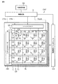
以下、本発明の第1実施形態に係る液晶表示装置について図面を参照して説明する。図1に示すように、本実施形態に係るに係る液晶表示装置はOCBモードの液晶表示パネルDP、この液晶表示パネルDPを照明するバックライトBL、および液晶表示パネルDPおよびバックライトBLを制御するコントローラCNTを備える。 Hereinafter, a liquid crystal display device according to a first embodiment of the present invention will be described with reference to the drawings. As shown in FIG. 1, the liquid crystal display device according to the present embodiment controls an OCB mode liquid crystal display panel DP, a backlight BL that illuminates the liquid crystal display panel DP, and the liquid crystal display panel DP and the backlight BL. A controller CNT is provided.
液晶表示パネルDPは一対の電極基板、すなわち、アレイ基板1および対向基板2と、アレイ基板1および対向基板2間に挟持された液晶層3とを有している。液晶層3は、例えば、ノーマリホワイトの表示動作のために、予めスプレイ配向からベンド配向に転移されるOCBモード液晶を液晶材料として含む。本実施形態では、液晶のベンド配向からスプレイ配向への逆転移は、黒表示に対応した駆動電圧を液晶層3に周期的に印加することにより阻止される。
The liquid crystal display panel DP has a pair of electrode substrates, that is, an
また、液晶表示パネルDPは、略マトリクス状に配置された表示画素PXからなる表示部を有している。アレイ基板1は、例えばガラス等の透明絶縁基板を有している。この透明絶縁基板上には、各表示画素PXに複数の画素電極PEが配置されている。
In addition, the liquid crystal display panel DP has a display unit composed of display pixels PX arranged in a substantially matrix shape. The
さらに、アレイ基板1は、複数の画素電極PEの行に沿って配置された複数の走査線G(G1〜Gm)、複数の画素電極PEの列に沿って配置された複数の信号線S(S1〜Sn)、および、これら走査線Gおよび信号線Sの交差位置近傍に配置され各々対応走査線Gを介して駆動されたときに対応信号線Sおよび対応画素電極PE間で導通する複数の画素スイッチWを有する。
Furthermore, the
各画素スイッチWは、例えば、薄膜トランジスタからなる。画素スイッチWのゲートが走査線Gに接続され、ソース−ドレインパスが信号線Sおよび画素電極PE間に接続されている。 Each pixel switch W is made of, for example, a thin film transistor. The gate of the pixel switch W is connected to the scanning line G, and the source-drain path is connected between the signal line S and the pixel electrode PE.
対向基板2は、例えば、ガラス等の透明絶縁基板上に配置された赤、緑、青の着色層からなるカラーフィルタ(図示せず)、および複数の画素電極PEに対向してカラーフィルタ上に配置される対向電極CE等を有している。
The
各画素電極PEおよび対向電極CEは例えばITO等の透明電極材料からなるとともに、互いに平行にラビング処理される配向膜でそれぞれ覆われている。各画素電極PEおよび対向電極CEは、画素電極PEおよび対向電極CEからの電界に対応した液晶分子配列に制御される液晶層3の一部である画素領域と共に表示画素PXを構成する。
Each pixel electrode PE and counter electrode CE are made of a transparent electrode material such as ITO, and are covered with alignment films that are rubbed in parallel to each other. Each pixel electrode PE and counter electrode CE constitute a display pixel PX together with a pixel region which is a part of the
複数の表示画素PXは各々画素電極PEおよび対向電極CE間に液晶容量Clcを有する。液晶容量Clcは、液晶材料の比誘電率、画素電極面積、液晶セルギャップによって決まるが、本実施形態に係る液晶表示装置においては画素の表示色による差はないものとする。また、画素電極PEに印加される電圧と、走査線Gと略平行に延びるように配置された補助容量線Cに印加される電圧とによって、補助容量Csが構成される。 Each of the plurality of display pixels PX has a liquid crystal capacitance Clc between the pixel electrode PE and the counter electrode CE. The liquid crystal capacitance Clc is determined by the relative dielectric constant of the liquid crystal material, the pixel electrode area, and the liquid crystal cell gap. In the liquid crystal display device according to the present embodiment, there is no difference depending on the display color of the pixel. Further, the auxiliary capacitance Cs is configured by the voltage applied to the pixel electrode PE and the voltage applied to the auxiliary capacitance line C disposed so as to extend substantially parallel to the scanning line G.
本実施形態に係る液晶表示装置では、補助容量Csは、カラーフィルタの色に対応した各色表示画素において異なる大きさとなっている。 In the liquid crystal display device according to the present embodiment, the auxiliary capacitance Cs has a different size in each color display pixel corresponding to the color of the color filter.
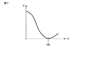
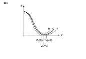
すなわち、黒表示に対応した電圧は、図7に示すように、液晶材料等の条件によって一意に決まる。しかし、カラー表示タイプの液晶表示装置の場合、図8に示したように、赤色表示画素における黒表示に対応した電圧Vb(R)、緑色表示画素における黒表示に対応した電圧Vb(G)、青色表示画素における黒表示に対応した電圧Vb(B)が異なる値となる。 That is, the voltage corresponding to black display is uniquely determined by the conditions of the liquid crystal material and the like as shown in FIG. However, in the case of a color display type liquid crystal display device, as shown in FIG. 8, a voltage Vb (R) corresponding to black display in a red display pixel, a voltage Vb (G) corresponding to black display in a green display pixel, The voltage Vb (B) corresponding to black display in the blue display pixel has a different value.
そこで、本実施形態に係る液晶表示装置では、赤色表示画素、青色表示画素、緑色表示画素のそれぞれに、異なる大きさの補助容量Cs(Cs(R)、Cs(G)、Cs(B))(図2を参照)を設け、単一の逆転移防止電圧を印加した場合であっても、各色表示画素それぞれが黒表示となるように設定している。 Therefore, in the liquid crystal display device according to the present embodiment, the auxiliary capacitors Cs (Cs (R), Cs (G), Cs (B)) having different sizes are provided for the red display pixel, the blue display pixel, and the green display pixel, respectively. (See FIG. 2), and even when a single reverse transition prevention voltage is applied, each color display pixel is set to display black.
具体的には、赤色表示画素、緑色表示画素、青色表示画素の各色表示画素において、補助容量Cs(x)は、下記数式1に基づき、Vb(x)=Vb(+) + dVd(x)=|Vb(−) − dVd(x)|となるように設定されている。

赤色表示画素、緑色表示画素、青色表示画素のそれぞれにおいて、逆転移防止電圧Vbの大きさが異なるため、上記のように設定された補助容量Csも各色表示画素のそれぞれにおいて異なる大きさとなる。 Since each of the red display pixel, the green display pixel, and the blue display pixel has a different reverse transition prevention voltage Vb, the auxiliary capacitance Cs set as described above has a different size for each color display pixel.
その結果、画素電圧Vdには、補助容量Cs(R)、Cs(G)、Cs(B)によって、赤色表示画素、緑色表示画素、青色表示画素のそれぞれの黒表示に対応した電圧とするような電圧が重畳される。 As a result, the pixel voltage Vd is set to a voltage corresponding to black display of each of the red display pixel, the green display pixel, and the blue display pixel by the auxiliary capacitors Cs (R), Cs (G), and Cs (B). A large voltage is superimposed.
上記のように各表示画素PXの補助容量Csの大きさを異ならせることによって、逆転移防止電圧として単一の黒表示に対応した電圧Vbを画素電極PEに印加した場合であっても、表示画素PXごとの透過率を略等しくすることができる。 Even if the voltage Vb corresponding to a single black display is applied to the pixel electrode PE as the reverse transition prevention voltage by making the size of the auxiliary capacitance Cs of each display pixel PX different as described above, display is possible. The transmittance for each pixel PX can be made substantially equal.
その結果、OCBモード液晶を有する液晶表示装置において、液晶の逆転移を防止するとともに、表示画像のコントラストの低下を防止し、動画視認性を向上させることができる。 As a result, in the liquid crystal display device having the OCB mode liquid crystal, the reverse transition of the liquid crystal can be prevented, the decrease in contrast of the display image can be prevented, and the moving image visibility can be improved.
コントローラCNTは、さらに複数の画素スイッチWを行単位に導通させるように複数の走査線G1〜Gmを順次駆動するゲートドライバGD、各行の画素スイッチWが対応走査線Gの駆動によって導通する期間において画素電圧Vdを複数の信号線S1〜Snにそれぞれ出力するソースドライバSD、バックライトBLを駆動するバックライト駆動部LD、およびゲートドライバGD、ソースドライバSDおよびバックライト駆動部(インバータ)LDを制御する制御回路5を備える。 The controller CNT further includes a gate driver GD that sequentially drives the plurality of scanning lines G1 to Gm so that the plurality of pixel switches W are conducted in units of rows, and a period in which the pixel switches W in each row are conducted by driving the corresponding scanning lines G. Controls the source driver SD that outputs the pixel voltage Vd to the plurality of signal lines S1 to Sn, the backlight driver LD that drives the backlight BL, and the gate driver GD, the source driver SD, and the backlight driver (inverter) LD, respectively. The control circuit 5 is provided.
制御回路5は電源投入時に対向電圧Vcomを変化させて比較的大きな駆動電圧を液晶層3に印加することにより液晶分子をスプレイ配向からベンド配向に転移させる初期化処理を行うように構成されている。
The control circuit 5 is configured to perform initialization processing for changing liquid crystal molecules from splay alignment to bend alignment by changing the counter voltage Vcom and applying a relatively large driving voltage to the
制御回路5は、外部信号源SSから入力される同期信号に基づいて発生される制御信号CTGをゲートドライバGDに出力し、外部信号源SSから入力される同期信号に基づいて発生される制御信号CTS、および外部信号源SSから入力される映像信号または黒挿入用の逆転移防止電圧をソースドライバSDに出力する。さらに、制御回路5は、対向電極CEに印加される対向電圧Vcomを対向基板CTの対向電極CEに対して出力する。 The control circuit 5 outputs a control signal CTG generated based on the synchronization signal input from the external signal source SS to the gate driver GD, and generates a control signal based on the synchronization signal input from the external signal source SS. The CTS and the video signal input from the external signal source SS or the reverse transition prevention voltage for black insertion are output to the source driver SD. Further, the control circuit 5 outputs a counter voltage Vcom applied to the counter electrode CE to the counter electrode CE of the counter substrate CT.
制御回路5では、外部信号源SSから入力される同期信号に基づき、第1期間および第2期間が設定される。第1期間は複数の表示画素PXに対して逆転移防止電圧Vbを書込む逆転移防止電圧書込を行うために用いられる。第2期間は複数の表示画素PXに対して映像信号Vsを書込む映像信号書込を行うために用いられる。第1期間および第2期間の合計時間長は1フレーム期間(1Fr)に等しい(図3参照)。 In the control circuit 5, the first period and the second period are set based on the synchronization signal input from the external signal source SS. The first period is used to perform reverse transition prevention voltage writing for writing the reverse transition prevention voltage Vb to the plurality of display pixels PX. The second period is used to perform video signal writing for writing the video signal Vs to the plurality of display pixels PX. The total time length of the first period and the second period is equal to one frame period (1Fr) (see FIG. 3).
ゲートドライバGDは、制御信号CTGの制御により、第1期間において複数の表示画素PXの行を逆転移防止電圧書込として順次選択するように複数の走査線G1〜Gmを順次駆動する。 The gate driver GD sequentially drives the plurality of scanning lines G1 to Gm so as to sequentially select the rows of the plurality of display pixels PX as reverse transition prevention voltage writing in the first period under the control of the control signal CTG.
第1期間に続く第2期間において、ゲートドライバGDは、複数の表示画素PXの行を映像信号書込走査として順次選択するように複数の走査線G1〜Gmを順次駆動する。 In the second period following the first period, the gate driver GD sequentially drives the plurality of scanning lines G1 to Gm so as to sequentially select the rows of the plurality of display pixels PX as video signal writing scans.
他方、ソースドライバSDは、第1期間において走査線G1〜Gmの各々が駆動される間に、1行分の逆転移防止電圧Vbを画素電圧Vdとして出力する。さらに、ソースドライバSDは、第2期間において走査線G1〜Gmの各々が駆動される間に、1行分の映像信号Vsを映像レベルの信号線入力電圧(ソース電圧)Vsoとして出力する。上記のように、ソースドライバSDは、並列的に複数の信号線S1〜Snを駆動する。 On the other hand, the source driver SD outputs the reverse transition prevention voltage Vb for one row as the pixel voltage Vd while each of the scanning lines G1 to Gm is driven in the first period. Further, the source driver SD outputs the video signal Vs for one row as the video level signal line input voltage (source voltage) Vso while each of the scanning lines G1 to Gm is driven in the second period. As described above, the source driver SD drives the plurality of signal lines S1 to Sn in parallel.
すなわち、本実施形態に係る液晶表示装置では、信号線S1〜Snの入力側がマルチプレクサMPXに接続されている。マルチプレクサMPXは、コントローラCNTの制御回路5によって制御され、ソースドライバSDの出力Vs、逆転移防止電圧Vb(+)、Vb(−)のいずれかを画素電圧Vdとして選択する(図2を参照)。なお、Vb(+)、Vb(−)はそれぞれ基準電圧Vcomに対して、各画素電位が正負となる場合の逆転移防止電圧印加時のソース電圧である。 That is, in the liquid crystal display device according to the present embodiment, the input sides of the signal lines S1 to Sn are connected to the multiplexer MPX. The multiplexer MPX is controlled by the control circuit 5 of the controller CNT, and selects one of the output Vs of the source driver SD, the reverse transition prevention voltage Vb (+), and Vb (−) as the pixel voltage Vd (see FIG. 2). . Vb (+) and Vb (−) are source voltages when a reverse transition prevention voltage is applied when each pixel potential is positive or negative with respect to the reference voltage Vcom.
ソース電圧Vsoは、対応する画素スイッチWを介して選択行の表示画素PXの画素電極PEに印加される。画素電極PEにおける画素電圧Vdと対向電極CEに印加された対向電圧Vcomによって、対向電極CEと画素電極PE間に液晶容量Clcが形成される。 The source voltage Vso is applied to the pixel electrode PE of the display pixel PX in the selected row via the corresponding pixel switch W. A liquid crystal capacitance Clc is formed between the counter electrode CE and the pixel electrode PE by the pixel voltage Vd at the pixel electrode PE and the counter voltage Vcom applied to the counter electrode CE.
このとき、本実施形態に係る液晶表示装置では、画素電圧Vdとしては補助容量Csによる電圧が重畳されている。すなわち、赤色表示画素では、画素電圧Vdに補助容量Cs(R)の大きさに応じた電圧が重畳されている。同様に、緑色表示画素および青色表示画素では、画素電圧Vdに補助容量Cs(G)および補助容量Cs(B)の大きさに応じた電圧が重畳されている。 At this time, in the liquid crystal display device according to the present embodiment, the voltage by the auxiliary capacitor Cs is superimposed as the pixel voltage Vd. That is, in the red display pixel, a voltage corresponding to the size of the auxiliary capacitor Cs (R) is superimposed on the pixel voltage Vd. Similarly, in the green display pixel and the blue display pixel, voltages corresponding to the sizes of the auxiliary capacitor Cs (G) and the auxiliary capacitor Cs (B) are superimposed on the pixel voltage Vd.
なお、全表示画素PXに対するソース電圧Vsoは、カラム反転駆動の場合には表示画素PXの列毎に逆極性に設定され、フレーム反転駆動の場合にはフレーム毎に逆極性に設定される。 Note that the source voltage Vso for all display pixels PX is set to a reverse polarity for each column of the display pixels PX in the case of column inversion driving, and is set to a reverse polarity for each frame in the case of frame inversion driving.
次に、上記の液晶表示装置の動作について以下に説明する。図3に示すように、ソースドライバSDは、1フレーム期間の第1期間において、信号線SLに逆転移防止電圧Vb(+)を出力する。 Next, the operation of the liquid crystal display device will be described below. As shown in FIG. 3, the source driver SD outputs the reverse transition prevention voltage Vb (+) to the signal line SL in the first period of one frame period.
このとき、ゲートドライバGDは、ゲート線GLを順次駆動する。ソース電圧Vso(x)は、ソース線S(x)に入力される映像信号であって、MPX(x)の制御により1フレーム(60Hz駆動であれば1/60sec)の前半を逆転移防止電圧Vb(+)あるいはVb(−)、後半を表示映像に応じた信号レベルを取る。 At this time, the gate driver GD sequentially drives the gate lines GL. The source voltage Vso (x) is a video signal input to the source line S (x), and the first half of one frame (1/60 sec for 60 Hz driving) is controlled by the MPX (x). Vb (+) or Vb (−), and the latter half takes a signal level corresponding to the display image.
ゲート電圧Vg1〜Vgmは、1〜m行目(mは液晶表示装置の走査線数)のゲート線Gに印加される電圧信号であり、1フレーム期間内に逆転移防止電圧と映像信号電圧とを表示画素PXに充電するため、第1期間と第2期間とのそれぞれにおいてオン電圧Vgonとなる。 The gate voltages Vg1 to Vgm are voltage signals applied to the gate lines G in the 1st to mth rows (m is the number of scanning lines of the liquid crystal display device), and the reverse transition prevention voltage and the video signal voltage are included in one frame period. Is charged to the display pixel PX, and the ON voltage Vgon is set in each of the first period and the second period.
補助容量電圧Vcs1〜Vcsmは、1〜m行目の補助容量線CsLに印加される電圧信号であって、表示画素PXに逆転移防止電圧あるいは映像信号電圧が充電された後、一定の電圧dVcsだけ信号レベルが変化する。 The auxiliary capacitance voltages Vcs1 to Vcsm are voltage signals applied to the auxiliary capacitance lines CsL in the 1st to m-th rows, and after the reverse transition prevention voltage or the video signal voltage is charged to the display pixel PX, the fixed voltage dVcs is set. Only the signal level changes.
Vd(x)は赤色表示画素、緑色表示画素、青色表示画素の各色表示画素の画素電圧(R、G、B)を示している。第1期間では、逆転移防止電圧Vb(+)あるいはVb(−)が充電される。第2期間では、各映像信号電圧Vsが充電される。 Vd (x) indicates the pixel voltage (R, G, B) of each color display pixel of the red display pixel, the green display pixel, and the blue display pixel. In the first period, the reverse transition prevention voltage Vb (+) or Vb (−) is charged. In the second period, each video signal voltage Vs is charged.
各色表示画素PXに、逆転移防止電圧Vb(+)、Vb(−)あるいは映像信号電圧Vsが充電された後に、さらに補助容量電圧の変化分dVcsによる電圧が重畳される。 After each color display pixel PX is charged with the reverse transition prevention voltage Vb (+), Vb (−) or the video signal voltage Vs, a voltage corresponding to the change dVcs of the auxiliary capacitance voltage is further superimposed.
このとき、重畳される電圧は、上記数式1にて表されるdVd(x)である。なお、容量Cdxは補助容量Cs(x)を除く表示画素の寄生容量の総和である。すなわち、赤色表示画素、緑色表示画素、青色表示画素のそれぞれにおいて、画素電圧Vd(x)には、補助容量Cs(R)、Cs(G)、Cs(B)の大きさに応じて、黒表示に対応した電圧とするような電圧が重畳される。
At this time, the superimposed voltage is dVd (x) expressed by the above
したがって、上記の液晶表示装置を図3に示すように駆動することによって、逆転移防止電圧Vb(x)を単一の信号電圧とした場合であっても、画素電圧Vdを各色表示画素における黒表示に対応した電圧とすることが可能になる。 Therefore, by driving the above-described liquid crystal display device as shown in FIG. 3, even when the reverse transition prevention voltage Vb (x) is a single signal voltage, the pixel voltage Vd is changed to black in each color display pixel. The voltage corresponding to the display can be set.
すなわち、本実施形態に係る液晶表示装置、および液晶表示装置の駆動方法によれば、表示品位の高いOCBモード液晶を用いた液晶表示装置を提供することができる。 That is, according to the liquid crystal display device and the driving method of the liquid crystal display device according to the present embodiment, a liquid crystal display device using OCB mode liquid crystal with high display quality can be provided.
次に、本発明の第2実施形態に係る液晶表示装置について図面を参照して以下に説明する。なお、以下の説明において、上述の第1実施形態に係る液晶表示装置と同様の構成については同一の符号を付して説明を省略する。 Next, a liquid crystal display device according to a second embodiment of the present invention will be described below with reference to the drawings. In the following description, the same components as those of the liquid crystal display device according to the first embodiment described above are denoted by the same reference numerals and description thereof is omitted.
図4及び図5に示すように、本実施形態に係る液晶表示装置では、互いに隣接する表示画素PXに対応する走査線Gに印加される電圧と画素電極PEに印加される電圧とによって補助容量Csが形成されている。 As shown in FIGS. 4 and 5, in the liquid crystal display device according to the present embodiment, the auxiliary capacitance is determined by the voltage applied to the scanning line G corresponding to the display pixels PX adjacent to each other and the voltage applied to the pixel electrode PE. Cs is formed.
すなわち、図5に示すように、走査線G(i)に印加される電圧によって導通する画素スイッチWを介して画素電圧Vdが印加される画素電極PEは、その隣接する行に配置された表示画素PXの画素電極PEに電圧を印加する走査線G(i−1)との間に補助容量Csを形成している。 That is, as shown in FIG. 5, the pixel electrode PE to which the pixel voltage Vd is applied via the pixel switch W that is turned on by the voltage applied to the scanning line G (i) is displayed in the adjacent row. An auxiliary capacitor Cs is formed between the scanning line G (i−1) for applying a voltage to the pixel electrode PE of the pixel PX.
本実施形態に係る液晶表示装置では、上述の第1実施形態と同様に、赤色表示画素、緑色表示画素、青色表示画素のそれぞれにおいて、異なる大きさの補助容量Cs(Cs(R)、Cs(G)、Cs(B))(図5を参照)が設けられ、単一の逆転移防止電圧を印加した場合であっても、各色表示画素それぞれが黒表示となるように設定される。 In the liquid crystal display device according to the present embodiment, as in the first embodiment described above, auxiliary capacitors Cs (Cs (R), Cs () having different sizes are respectively used for the red display pixel, the green display pixel, and the blue display pixel. G) and Cs (B)) (see FIG. 5) are provided, and each color display pixel is set to display black even when a single reverse transition prevention voltage is applied.
すなわち、上述の第1実施形態に係る液晶表示装置の場合と同様に、赤色表示画素、緑色表示画素、青色表示画素の各色表示画素において、補助容量Cs(x)は、上記数式1に基づき、Vb(x)=Vb(+) + dVd(x)=|Vb(−) − dVd(x)|となるように設定されている。
That is, as in the case of the liquid crystal display device according to the first embodiment described above, in each color display pixel of the red display pixel, the green display pixel, and the blue display pixel, the auxiliary capacitance Cs (x) is based on
赤色表示画素、緑色表示画素、青色表示画素のそれぞれにおいて、逆転移防止電圧Vbの大きさが異なるため、補助容量Csも異なる大きさとなる。その結果、画素電圧Vdには、補助容量Cs(R)、Cs(G)、Cs(B)によって、赤色表示画素、緑色表示画素、青色表示画素のそれぞれの黒表示に対応した電圧とするような電圧が重畳される。 Since each of the red display pixel, the green display pixel, and the blue display pixel has a different reverse transition prevention voltage Vb, the auxiliary capacitance Cs also has a different size. As a result, the pixel voltage Vd is set to a voltage corresponding to black display of each of the red display pixel, the green display pixel, and the blue display pixel by the auxiliary capacitors Cs (R), Cs (G), and Cs (B). A large voltage is superimposed.
上記の液晶表示装置の駆動方法を図6に示す。すなわち、ソースドライバSDは、1フレーム期間の第1期間において信号線S(x)に逆転移防止電圧Vbを印加する。なお、本実施形態に係る液晶表示装置では、上述の第1実施形態の場合と同様に、逆転移防止電圧Vbとして黒表示に対応した電圧を印加している。ソースドライバSDは、1フレーム期間の第2期間において、信号線S(x)に映像信号を印加する。 A driving method of the liquid crystal display device is shown in FIG. That is, the source driver SD applies the reverse transition prevention voltage Vb to the signal line S (x) in the first period of one frame period. In the liquid crystal display device according to the present embodiment, a voltage corresponding to black display is applied as the reverse transition prevention voltage Vb, as in the case of the first embodiment described above. The source driver SD applies a video signal to the signal line S (x) in the second period of one frame period.
ゲートドライバGDは、画素充電後に、前段のゲート信号Vg(i−1)をdVg(=dVcs)だけ変化させる、このことによって、各色表示画素の電圧重畳後の逆転移防止電圧Vbを単一の信号電圧とした場合であっても、画素電圧Vdを各色表示画素における黒表示に対応した電圧とすることが可能になる。 The gate driver GD changes the gate signal Vg (i−1) of the previous stage by dVg (= dVcs) after pixel charging, whereby the reverse transition prevention voltage Vb after voltage superposition of each color display pixel is changed to a single value. Even when the signal voltage is used, the pixel voltage Vd can be set to a voltage corresponding to black display in each color display pixel.
すなわち、本実施形態に係る液晶表示装置および液晶表示装置の駆動方法によれば、上述の第1実施形態に係る液晶表示装置と同様に、表示品位の高いOCBモード液晶を用いた液晶表示装置を提供することができる。 That is, according to the liquid crystal display device and the driving method of the liquid crystal display device according to the present embodiment, the liquid crystal display device using the OCB mode liquid crystal with high display quality is provided as in the liquid crystal display device according to the first embodiment. Can be provided.
なお、この発明は、上記実施形態そのままに限定されるものではなく、実施段階ではその要旨を逸脱しない範囲で構成要素を変形して具体化できる。 Note that the present invention is not limited to the above-described embodiment as it is, and can be embodied by modifying the constituent elements without departing from the scope of the invention in the implementation stage.
また、上記実施形態に開示されている複数の構成要素の適宜な組み合せにより種々の発明を形成できる。例えば、実施形態に示される全構成要素から幾つかの構成要素を削除してもよい。更に、異なる実施形態に亘る構成要素を適宜組み合わせてもよい。 Further, various inventions can be formed by appropriately combining a plurality of constituent elements disclosed in the embodiment. For example, some components may be deleted from all the components shown in the embodiment. Furthermore, you may combine the component covering different embodiment suitably.
PX…表示画素、PE…画素電極、G…ゲート線、S…ソース線、W…画素スイッチ、CE…対向電極、Clc…液晶容量、C…補助容量線、Cs…補助容量、Vb…逆転移防止電圧、Vd…画素電圧、1…アレイ基板、2…対向基板 PX ... display pixel, PE ... pixel electrode, G ... gate line, S ... source line, W ... pixel switch, CE ... counter electrode, Clc ... liquid crystal capacitor, C ... auxiliary capacitor line, Cs ... auxiliary capacitor, Vb ... reverse transition Prevention voltage, Vd ... pixel voltage, 1 ... array substrate, 2 ... counter substrate
Claims (6)
前記複数の表示画素のそれぞれに対応するように複数の画素電極が配置された第1基板と、
前記複数の画素電極に対向した対向電極が配置された第2基板と、
前記第1基板および前記第2基板間に挟持された液晶層と、
前記第1基板および前記第2基板のいずれか一方に配置されたカラーフィルタと、を備え、
前記表示画素は、前記カラーフィルタの色に応じた複数種類の色表示画素を有し、
前記第1基板は前記画素電極および前記対向電極間の電位により生じる液晶容量と結合する補助容量を有し、
前記補助容量は、前記複数種類の色表示画素それぞれにおいて異なる大きさである液晶表示装置。 A liquid crystal display device comprising a display unit comprising a plurality of display pixels arranged in a matrix,
A first substrate on which a plurality of pixel electrodes are arranged so as to correspond to each of the plurality of display pixels;
A second substrate on which a counter electrode facing the plurality of pixel electrodes is disposed;
A liquid crystal layer sandwiched between the first substrate and the second substrate;
A color filter disposed on one of the first substrate and the second substrate,
The display pixel has a plurality of types of color display pixels according to the color of the color filter,
The first substrate has a storage capacitor coupled with a liquid crystal capacitor generated by a potential between the pixel electrode and the counter electrode;
The auxiliary capacitor is a liquid crystal display device having a different size in each of the plurality of types of color display pixels.
前記表示画素の配列する行に沿って配置された複数の走査線と、
前記複数の走査線と平行に延びた補助容量線と、が配置され、
前記補助容量は、前記画素電極に印加される電圧と前記補助容量線に印加される電圧とによって形成される請求項1記載の液晶表示装置。 The display unit includes a plurality of signal lines arranged along a column in which the display pixels are arranged,
A plurality of scanning lines arranged along rows of the display pixels;
An auxiliary capacitance line extending in parallel with the plurality of scanning lines is disposed,
The liquid crystal display device according to claim 1, wherein the auxiliary capacitance is formed by a voltage applied to the pixel electrode and a voltage applied to the auxiliary capacitance line.
前記表示画素の配列する行に沿って配置された複数の走査線と、が配置され、
前記補助容量は、隣接する表示画素に走査信号を供給する走査線に印加される電圧と、前記画素電極に印加される電圧とによって形成される請求項1記載の液晶表示装置。 In the display unit, a plurality of signal lines positioned along a column in which the display pixels are arranged, and
A plurality of scanning lines arranged along a row in which the display pixels are arranged, and
The liquid crystal display device according to claim 1, wherein the auxiliary capacitor is formed by a voltage applied to a scanning line that supplies a scanning signal to an adjacent display pixel and a voltage applied to the pixel electrode.
1フレーム期間の第1期間において、前記第1基板上の前記表示画素のそれぞれに配置された画素電極に逆転移防止電圧を印加し、
画素充電後に、前記画素電極と前記画素電極と対向して配置された対向電極との間に生じる液晶容量と結合する補助容量に印加する電圧の大きさを一定値変化させ、
1フレーム期間の第2期間において、前記画素電極に映像信号を印加し、
画素充電後に、前記補助容量に印加する電圧の大きさを一定値変化させ、前記カラーフィルタの色に対応した複数種類の色表示画素毎に前記補助容量の大きさを変化させる液晶表示装置の駆動方法。 A first substrate; a second substrate disposed opposite to the first substrate; a liquid crystal layer sandwiched between the first substrate and the second substrate; and a plurality of displays disposed in a matrix A method for driving a liquid crystal display device comprising: a display unit including pixels; and a color filter disposed on one of the first substrate and the second substrate,
In the first period of one frame period, a reverse transition prevention voltage is applied to the pixel electrode disposed in each of the display pixels on the first substrate,
After pixel charging, the magnitude of the voltage applied to the auxiliary capacitor combined with the liquid crystal capacitor generated between the pixel electrode and the counter electrode arranged to face the pixel electrode is changed by a certain value,
In the second period of one frame period, a video signal is applied to the pixel electrode,
Driving a liquid crystal display device that changes the magnitude of the voltage applied to the auxiliary capacitor after pixel charging by a constant value and changes the size of the auxiliary capacitor for each of a plurality of types of color display pixels corresponding to the color of the color filter. Method.
Priority Applications (1)
| Application Number | Priority Date | Filing Date | Title |
|---|---|---|---|
| JP2007124732A JP2008281702A (en) | 2007-05-09 | 2007-05-09 | Liquid crystal display device and method for driving liquid crystal display device |
Applications Claiming Priority (1)
| Application Number | Priority Date | Filing Date | Title |
|---|---|---|---|
| JP2007124732A JP2008281702A (en) | 2007-05-09 | 2007-05-09 | Liquid crystal display device and method for driving liquid crystal display device |
Publications (1)
| Publication Number | Publication Date |
|---|---|
| JP2008281702A true JP2008281702A (en) | 2008-11-20 |
Family
ID=40142584
Family Applications (1)
| Application Number | Title | Priority Date | Filing Date |
|---|---|---|---|
| JP2007124732A Pending JP2008281702A (en) | 2007-05-09 | 2007-05-09 | Liquid crystal display device and method for driving liquid crystal display device |
Country Status (1)
| Country | Link |
|---|---|
| JP (1) | JP2008281702A (en) |
Cited By (3)
| Publication number | Priority date | Publication date | Assignee | Title |
|---|---|---|---|---|
| JP2011033956A (en) * | 2009-08-05 | 2011-02-17 | Seiko Epson Corp | Liquid crystal device, circuit and method for driving of pixel, and electronic apparatus |
| WO2012002073A1 (en) * | 2010-06-28 | 2012-01-05 | シャープ株式会社 | Display panel and display unit |
| JP2013117680A (en) * | 2011-12-05 | 2013-06-13 | Japan Display Central Co Ltd | Liquid crystal display device and driving method for the same |
-
2007
- 2007-05-09 JP JP2007124732A patent/JP2008281702A/en active Pending
Cited By (4)
| Publication number | Priority date | Publication date | Assignee | Title |
|---|---|---|---|---|
| JP2011033956A (en) * | 2009-08-05 | 2011-02-17 | Seiko Epson Corp | Liquid crystal device, circuit and method for driving of pixel, and electronic apparatus |
| WO2012002073A1 (en) * | 2010-06-28 | 2012-01-05 | シャープ株式会社 | Display panel and display unit |
| JP2013117680A (en) * | 2011-12-05 | 2013-06-13 | Japan Display Central Co Ltd | Liquid crystal display device and driving method for the same |
| US8976100B2 (en) | 2011-12-05 | 2015-03-10 | Japan Display Inc. | Liquid crystal display having a transition from splay alignment to bend alignment and driving method thereof |
Similar Documents
| Publication | Publication Date | Title |
|---|---|---|
| JP2005234544A (en) | Liquid crystal display device and its driving method | |
| US10089950B2 (en) | Electro-optical device, method of controlling electro-optical device, and electronic instrument | |
| JP5290419B2 (en) | Active matrix substrate, liquid crystal panel, liquid crystal display device, liquid crystal display unit, television receiver | |
| US8289255B2 (en) | Electro-optical apparatus and display thereof | |
| JP2010266738A (en) | Liquid crystal display device and method of driving the same | |
| US20160118002A1 (en) | Electro-optic apparatus, control method for electro-optic apparatus, and electronic device | |
| JP5121334B2 (en) | Liquid crystal display device and driving method of liquid crystal display device | |
| JP4342538B2 (en) | Liquid crystal display device and driving method of liquid crystal display device | |
| JP4178977B2 (en) | Display drive device and drive control method thereof, and active matrix liquid crystal display device and drive method thereof. | |
| JP2009244287A (en) | Liquid crystal display and method of driving liquid crystal display | |
| JP5035888B2 (en) | Liquid crystal display device and driving method of liquid crystal display device | |
| JP2008281702A (en) | Liquid crystal display device and method for driving liquid crystal display device | |
| US9489910B2 (en) | Display device | |
| KR20160091528A (en) | Display device and driving method for display device using the same | |
| US10665201B2 (en) | Display device | |
| JP5803483B2 (en) | Liquid crystal display device, driving method thereof, and electronic apparatus | |
| JP2007156013A (en) | Liquid crystal display panel | |
| JP5588958B2 (en) | Liquid crystal display device and driving method of liquid crystal display device | |
| JP2009244285A (en) | Liquid crystal display and method of driving liquid crystal display | |
| JP4974029B2 (en) | Liquid crystal display | |
| JP2010008576A (en) | Liquid crystal display, and method of driving liquid crystal display | |
| JP2009037072A (en) | Liquid crystal display, and drive method for the liquid crystal display | |
| US20210065638A1 (en) | Display device | |
| US8264439B2 (en) | Liquid crystal display panel and liquid crystal display device using the same | |
| JP2010113148A (en) | Liquid crystal display |