JP2007300088A - 複数の金属層から形成される半導体素子パッケージリードフレーム - Google Patents
複数の金属層から形成される半導体素子パッケージリードフレーム Download PDFInfo
- Publication number
- JP2007300088A JP2007300088A JP2007104458A JP2007104458A JP2007300088A JP 2007300088 A JP2007300088 A JP 2007300088A JP 2007104458 A JP2007104458 A JP 2007104458A JP 2007104458 A JP2007104458 A JP 2007104458A JP 2007300088 A JP2007300088 A JP 2007300088A
- Authority
- JP
- Japan
- Prior art keywords
- metal layer
- lead frame
- package
- die
- semiconductor device
- Prior art date
- Legal status (The legal status is an assumption and is not a legal conclusion. Google has not performed a legal analysis and makes no representation as to the accuracy of the status listed.)
- Pending
Links
Images


Classifications
-
- H—ELECTRICITY
- H10—SEMICONDUCTOR DEVICES; ELECTRIC SOLID-STATE DEVICES NOT OTHERWISE PROVIDED FOR
- H10W—GENERIC PACKAGES, INTERCONNECTIONS, CONNECTORS OR OTHER CONSTRUCTIONAL DETAILS OF DEVICES COVERED BY CLASS H10
- H10W90/00—Package configurations
- H10W90/701—Package configurations characterised by the relative positions of pads or connectors relative to package parts
- H10W90/721—Package configurations characterised by the relative positions of pads or connectors relative to package parts of bump connectors
- H10W90/726—Package configurations characterised by the relative positions of pads or connectors relative to package parts of bump connectors between a chip and a stacked lead frame, conducting package substrate or heat sink
-
- H—ELECTRICITY
- H10—SEMICONDUCTOR DEVICES; ELECTRIC SOLID-STATE DEVICES NOT OTHERWISE PROVIDED FOR
- H10W—GENERIC PACKAGES, INTERCONNECTIONS, CONNECTORS OR OTHER CONSTRUCTIONAL DETAILS OF DEVICES COVERED BY CLASS H10
- H10W90/00—Package configurations
- H10W90/701—Package configurations characterised by the relative positions of pads or connectors relative to package parts
- H10W90/751—Package configurations characterised by the relative positions of pads or connectors relative to package parts of bond wires
- H10W90/756—Package configurations characterised by the relative positions of pads or connectors relative to package parts of bond wires between a chip and a stacked lead frame, conducting package substrate or heat sink
Landscapes
- Lead Frames For Integrated Circuits (AREA)
Applications Claiming Priority (1)
| Application Number | Priority Date | Filing Date | Title |
|---|---|---|---|
| US11/416,994 US20070130759A1 (en) | 2005-06-15 | 2006-05-02 | Semiconductor device package leadframe formed from multiple metal layers |
Publications (2)
| Publication Number | Publication Date |
|---|---|
| JP2007300088A true JP2007300088A (ja) | 2007-11-15 |
| JP2007300088A5 JP2007300088A5 (https=) | 2011-06-23 |
Family
ID=38769289
Family Applications (1)
| Application Number | Title | Priority Date | Filing Date |
|---|---|---|---|
| JP2007104458A Pending JP2007300088A (ja) | 2006-05-02 | 2007-04-12 | 複数の金属層から形成される半導体素子パッケージリードフレーム |
Country Status (2)
| Country | Link |
|---|---|
| JP (1) | JP2007300088A (https=) |
| CN (1) | CN101068005B (https=) |
Cited By (2)
| Publication number | Priority date | Publication date | Assignee | Title |
|---|---|---|---|---|
| CN102117752A (zh) * | 2010-10-15 | 2011-07-06 | 日月光半导体制造股份有限公司 | 引脚框架封装结构及其制作方法 |
| US10847700B2 (en) | 2018-06-25 | 2020-11-24 | Nichia Corporation | Package, light emitting device, method of manufacturing package, and method of manufacturing light emitting device |
Families Citing this family (6)
| Publication number | Priority date | Publication date | Assignee | Title |
|---|---|---|---|---|
| CN101521164B (zh) * | 2008-02-26 | 2011-01-05 | 上海凯虹科技电子有限公司 | 引线键合芯片级封装方法 |
| CN102915988A (zh) * | 2012-10-31 | 2013-02-06 | 矽力杰半导体技术(杭州)有限公司 | 一种引线框架以及应用其的倒装封装装置 |
| CN103928431B (zh) * | 2012-10-31 | 2017-03-01 | 矽力杰半导体技术(杭州)有限公司 | 一种倒装封装装置 |
| CN103594448A (zh) * | 2013-11-15 | 2014-02-19 | 杰群电子科技(东莞)有限公司 | 一种引线框架 |
| CN110524891A (zh) * | 2018-05-24 | 2019-12-03 | 本田技研工业株式会社 | 连续超声波增材制造 |
| US11298775B2 (en) | 2018-05-24 | 2022-04-12 | Honda Motor Co., Ltd. | Continuous ultrasonic additive manufacturing |
Family Cites Families (3)
| Publication number | Priority date | Publication date | Assignee | Title |
|---|---|---|---|---|
| JP2582013B2 (ja) * | 1991-02-08 | 1997-02-19 | 株式会社東芝 | 樹脂封止型半導体装置及びその製造方法 |
| US6983537B2 (en) * | 2000-07-25 | 2006-01-10 | Mediana Electronic Co., Ltd. | Method of making a plastic package with an air cavity |
| JP2004281887A (ja) * | 2003-03-18 | 2004-10-07 | Himeji Toshiba Ep Corp | リードフレーム及びそれを用いた電子部品 |
-
2007
- 2007-04-09 CN CN200710090879.3A patent/CN101068005B/zh active Active
- 2007-04-12 JP JP2007104458A patent/JP2007300088A/ja active Pending
Cited By (2)
| Publication number | Priority date | Publication date | Assignee | Title |
|---|---|---|---|---|
| CN102117752A (zh) * | 2010-10-15 | 2011-07-06 | 日月光半导体制造股份有限公司 | 引脚框架封装结构及其制作方法 |
| US10847700B2 (en) | 2018-06-25 | 2020-11-24 | Nichia Corporation | Package, light emitting device, method of manufacturing package, and method of manufacturing light emitting device |
Also Published As
| Publication number | Publication date |
|---|---|
| CN101068005A (zh) | 2007-11-07 |
| CN101068005B (zh) | 2010-12-29 |
Similar Documents
| Publication | Publication Date | Title |
|---|---|---|
| US6720207B2 (en) | Leadframe, resin-molded semiconductor device including the leadframe, method of making the leadframe and method for manufacturing the device | |
| US9087827B2 (en) | Mixed wire semiconductor lead frame package | |
| US7026192B2 (en) | Terminal land frame and method for manufacturing the same | |
| US9698143B2 (en) | Wireless module with active devices | |
| US7132315B2 (en) | Leadframe, plastic-encapsulated semiconductor device, and method for fabricating the same | |
| US7691681B2 (en) | Chip scale package having flip chip interconnect on die paddle | |
| US20050260795A1 (en) | Method for fabricating leadless packages with mold locking characteristics | |
| JP2007300088A (ja) | 複数の金属層から形成される半導体素子パッケージリードフレーム | |
| DE112006001663T5 (de) | Halbleiterchip-Gehäuse und Verfahren zur Herstellung desselben | |
| KR101293685B1 (ko) | 반도체 디바이스용 높은 접착 라인 두께 | |
| JP2009094118A (ja) | リードフレーム、それを備える電子部品及びその製造方法 | |
| CN115605991A (zh) | 包含具有暴露背侧金属的下安装式裸片的半导体封装 | |
| US8106491B2 (en) | Methods of forming stacked semiconductor devices with a leadframe and associated assemblies | |
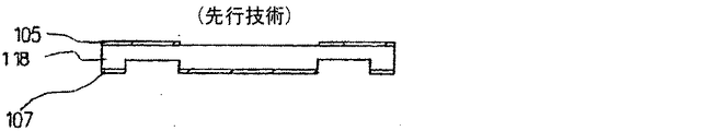
| US20070130759A1 (en) | Semiconductor device package leadframe formed from multiple metal layers | |
| JP3460646B2 (ja) | 樹脂封止型半導体装置およびその製造方法 | |
| KR101753416B1 (ko) | Ic 패키지용 리드프레임 및 제조방법 | |
| JP2010050288A (ja) | 樹脂封止型半導体装置およびその製造方法 | |
| JP2007287762A (ja) | 半導体集積回路素子とその製造方法および半導体装置 | |
| JP2006032871A (ja) | 半導体装置 | |
| JP3699966B2 (ja) | リードフレーム,樹脂封止型半導体装置及びその製造方法 | |
| JP3965813B2 (ja) | ターミナルランドフレームの製造方法 | |
| JP2006279088A (ja) | 半導体装置の製造方法 | |
| JP2006093556A (ja) | 半導体装置及びその製造方法 | |
| JP2005252314A (ja) | リードフレーム,樹脂封止型半導体装置及びその製造方法 | |
| JP2010129758A (ja) | 半導体装置及びその製造方法 |
Legal Events
| Date | Code | Title | Description |
|---|---|---|---|
| A521 | Request for written amendment filed |
Free format text: JAPANESE INTERMEDIATE CODE: A523 Effective date: 20071219 |
|
| A621 | Written request for application examination |
Free format text: JAPANESE INTERMEDIATE CODE: A621 Effective date: 20100408 |
|
| A521 | Request for written amendment filed |
Free format text: JAPANESE INTERMEDIATE CODE: A523 Effective date: 20110401 |
|
| A521 | Request for written amendment filed |
Free format text: JAPANESE INTERMEDIATE CODE: A523 Effective date: 20110511 |
|
| A977 | Report on retrieval |
Free format text: JAPANESE INTERMEDIATE CODE: A971007 Effective date: 20120416 |
|
| A131 | Notification of reasons for refusal |
Free format text: JAPANESE INTERMEDIATE CODE: A131 Effective date: 20120620 |
|
| A521 | Request for written amendment filed |
Free format text: JAPANESE INTERMEDIATE CODE: A523 Effective date: 20120919 |
|
| A02 | Decision of refusal |
Free format text: JAPANESE INTERMEDIATE CODE: A02 Effective date: 20130530 |