JP2007158253A - Heat treatment equipment - Google Patents
Heat treatment equipment Download PDFInfo
- Publication number
- JP2007158253A JP2007158253A JP2005355183A JP2005355183A JP2007158253A JP 2007158253 A JP2007158253 A JP 2007158253A JP 2005355183 A JP2005355183 A JP 2005355183A JP 2005355183 A JP2005355183 A JP 2005355183A JP 2007158253 A JP2007158253 A JP 2007158253A
- Authority
- JP
- Japan
- Prior art keywords
- substrate
- heat treatment
- casing
- planar heaters
- planar
- Prior art date
- Legal status (The legal status is an assumption and is not a legal conclusion. Google has not performed a legal analysis and makes no representation as to the accuracy of the status listed.)
- Granted
Links
Images


Classifications
-
- H—ELECTRICITY
- H01—ELECTRIC ELEMENTS
- H01L—SEMICONDUCTOR DEVICES NOT COVERED BY CLASS H10
- H01L21/00—Processes or apparatus adapted for the manufacture or treatment of semiconductor or solid state devices or of parts thereof
- H01L21/67—Apparatus specially adapted for handling semiconductor or electric solid state devices during manufacture or treatment thereof; Apparatus specially adapted for handling wafers during manufacture or treatment of semiconductor or electric solid state devices or components ; Apparatus not specifically provided for elsewhere
- H01L21/67005—Apparatus not specifically provided for elsewhere
- H01L21/67011—Apparatus for manufacture or treatment
- H01L21/67098—Apparatus for thermal treatment
- H01L21/67109—Apparatus for thermal treatment mainly by convection
-
- H—ELECTRICITY
- H01—ELECTRIC ELEMENTS
- H01L—SEMICONDUCTOR DEVICES NOT COVERED BY CLASS H10
- H01L21/00—Processes or apparatus adapted for the manufacture or treatment of semiconductor or solid state devices or of parts thereof
- H01L21/67—Apparatus specially adapted for handling semiconductor or electric solid state devices during manufacture or treatment thereof; Apparatus specially adapted for handling wafers during manufacture or treatment of semiconductor or electric solid state devices or components ; Apparatus not specifically provided for elsewhere
- H01L21/67005—Apparatus not specifically provided for elsewhere
- H01L21/67011—Apparatus for manufacture or treatment
- H01L21/67155—Apparatus for manufacturing or treating in a plurality of work-stations
- H01L21/67161—Apparatus for manufacturing or treating in a plurality of work-stations characterized by the layout of the process chambers
- H01L21/67173—Apparatus for manufacturing or treating in a plurality of work-stations characterized by the layout of the process chambers in-line arrangement
-
- H—ELECTRICITY
- H01—ELECTRIC ELEMENTS
- H01L—SEMICONDUCTOR DEVICES NOT COVERED BY CLASS H10
- H01L21/00—Processes or apparatus adapted for the manufacture or treatment of semiconductor or solid state devices or of parts thereof
- H01L21/67—Apparatus specially adapted for handling semiconductor or electric solid state devices during manufacture or treatment thereof; Apparatus specially adapted for handling wafers during manufacture or treatment of semiconductor or electric solid state devices or components ; Apparatus not specifically provided for elsewhere
- H01L21/67005—Apparatus not specifically provided for elsewhere
- H01L21/67011—Apparatus for manufacture or treatment
- H01L21/67155—Apparatus for manufacturing or treating in a plurality of work-stations
- H01L21/67207—Apparatus for manufacturing or treating in a plurality of work-stations comprising a chamber adapted to a particular process
Landscapes
- Engineering & Computer Science (AREA)
- Microelectronics & Electronic Packaging (AREA)
- Condensed Matter Physics & Semiconductors (AREA)
- General Physics & Mathematics (AREA)
- Manufacturing & Machinery (AREA)
- Computer Hardware Design (AREA)
- Physics & Mathematics (AREA)
- Power Engineering (AREA)
- Exposure Of Semiconductors, Excluding Electron Or Ion Beam Exposure (AREA)
- Container, Conveyance, Adherence, Positioning, Of Wafer (AREA)
- Resistance Heating (AREA)
- Control Of Resistance Heating (AREA)
- Tunnel Furnaces (AREA)
Abstract
Description
本発明は、フラットパネルディスプレイ(FPD)用のガラス基板等の基板に加熱処理を施す加熱処理装置に関する。 The present invention relates to a heat treatment apparatus for performing heat treatment on a substrate such as a glass substrate for a flat panel display (FPD).
FPDの製造においては、FPD用のガラス基板上に回路パターンを形成するためにフォトリソグラフィ技術が用いられる。フォトリソグラフィによる回路パターンの形成は、ガラス基板上にレジスト液を塗布してレジスト膜を形成し、回路パターンに対応するようにレジスト膜を露光し、これを現像処理するといった手順で行われる。 In manufacturing an FPD, a photolithography technique is used to form a circuit pattern on a glass substrate for FPD. The circuit pattern is formed by photolithography by applying a resist solution on a glass substrate to form a resist film, exposing the resist film so as to correspond to the circuit pattern, and developing the resist film.
フォトリソグラフィ技術では一般的に、レジスト膜の形成後および現像処理後に、レジスト膜を乾燥させるためにガラス基板に対して加熱処理が施される。このような加熱処理には、ガラス基板を収容可能なケーシングと、ケーシング内に設けられた、ガラス基板を載置して加熱する加熱プレートと、加熱プレート上から突出および没入するように昇降可能に設けられ、搬送アームにより把持されて搬送されたガラス基板を加熱プレート上に受け渡す昇降ピンとを具備した加熱処理装置が用いられている(例えば特許文献1、2、3参照)。 In the photolithography technique, generally, after the resist film is formed and developed, a heat treatment is performed on the glass substrate in order to dry the resist film. In such a heat treatment, a casing capable of accommodating a glass substrate, a heating plate provided in the casing for placing and heating the glass substrate, and raising and lowering so as to protrude and immerse from the heating plate can be performed. There is used a heat treatment apparatus that includes a lift pin that is provided and transfers a glass substrate held and conveyed by a transfer arm onto a heating plate (for example, see Patent Documents 1, 2, and 3).
ところで、近時、FPDの大型化が指向され、一辺が2m以上にもなる巨大なガラス基板が出現するに至っている。これに対して、上述した従来の加熱処理装置では、ガラス基板の加熱手段がガラス基板を載置する加熱プレートであるため、ガラス基板が大型になると、基板全体を均等に加熱することが難しくなり、加熱処理によってガラス基板に反りが生じてしまうおそれがある。また、ガラス基板は大型化に伴って取り扱い性が悪くなるため、この加熱処理装置では、ガラス基板が大型になると、搬送アームと昇降ピンとの間または昇降ピンと加熱プレートとの間の受け渡しの際の衝撃によって破損してしまうおそれもある。 By the way, recently, the enlargement of FPD has been directed and a huge glass substrate having a side of 2 m or more has appeared. On the other hand, in the conventional heat treatment apparatus described above, since the heating means for the glass substrate is a heating plate for placing the glass substrate, when the glass substrate becomes large, it becomes difficult to uniformly heat the entire substrate. The glass substrate may be warped by the heat treatment. In addition, since the glass substrate becomes difficult to handle as the size of the glass substrate increases, in this heat treatment apparatus, when the glass substrate becomes large, when the glass substrate becomes large, it is necessary to transfer between the transfer arm and the lifting pins or between the lifting pins and the heating plate. There is also a risk of damage due to impact.
その一方で、加熱処理装置では、基板の大型化に伴う装置自体の著しい巨大化を回避するため、ケーシング内の基板周りのスペースを極力小さく抑えてケーシングを小型化することが望まれている。
本発明は、かかる事情に鑑みてなされたものであって、基板が大型であっても基板の反りや破損等の不具合の発生を抑止することができるとともに、基板を収容するケーシングの小型化を図ることが可能な加熱処理装置の提供を目的とする。 The present invention has been made in view of such circumstances, and even if the substrate is large, it is possible to suppress the occurrence of problems such as warping and breakage of the substrate, and to reduce the size of the casing that accommodates the substrate. It is an object of the present invention to provide a heat treatment apparatus that can be used.
上記課題を解決するために、本発明は、基板に加熱処理を施す加熱処理装置であって、基板を一方向に搬送する搬送路と、前記搬送路を囲繞するように設けられたケーシングと、前記搬送路に沿って前記ケーシング内に、前記搬送路を搬送される基板に近接するように基板の両面側にそれぞれ設けられた第1および第2の面状ヒーターとを具備することを特徴とする加熱処理装置を提供する。 In order to solve the above problems, the present invention is a heat treatment apparatus for performing heat treatment on a substrate, a conveyance path for conveying the substrate in one direction, a casing provided so as to surround the conveyance path, The first and second planar heaters respectively provided on both sides of the substrate so as to be close to the substrate conveyed along the conveyance path in the casing along the conveyance path. A heat treatment apparatus is provided.
本発明において、前記搬送路は、一方向に間隔をあけて複数設けられたコロ部材の回転によって基板をコロ搬送し、前記第1の面状ヒーターは、前記コロ部材同士の間にそれぞれ設けられて搬送方向に複数配列されていることが好ましい。この場合に、前記第2の面状ヒーターは、前記第1の面状ヒーターの配列ピッチと対応するように搬送方向に複数配列され、前記複数の第1および第2の面状ヒーターは、個別または搬送方向に区分けされたグループごとに温度制御可能であることが好ましい。さらに、この場合に、前記複数の第1および第2の面状ヒーターが、個別または搬送方向に区分けされたグループごとに温度制御されることにより、前記複数の第1および第2の面状ヒーターからなるヒーター群は所定の温度プロファイルを形成することが好ましく、前記第1および第2の面状ヒーターはそれぞれ、前記搬送路の幅方向に複数に区分けされた領域ごとに温度制御可能であることが好ましく、前記第2の面状ヒーターは、前記ケーシングの一壁部に取り付けられており、前記ケーシングの前記一壁部は、前記ケーシング内を開閉する扉として機能することが好ましい。また、これらの場合に、前記コロ部材は、少なくとも外周面が熱伝導率の低い材料からなることが好ましい。 In the present invention, the transport path rolls the substrate by rotating a plurality of roller members provided at intervals in one direction, and the first planar heaters are provided between the roller members, respectively. It is preferable that a plurality are arranged in the transport direction. In this case, a plurality of the second planar heaters are arranged in the transport direction so as to correspond to the arrangement pitch of the first planar heaters, and the plurality of first and second planar heaters are individually provided. Alternatively, it is preferable that the temperature can be controlled for each group divided in the transport direction. Further, in this case, the plurality of first and second planar heaters are temperature-controlled individually or for each group divided in the transport direction, thereby the plurality of first and second planar heaters. It is preferable that the heater group consisting of the above-mentioned heaters forms a predetermined temperature profile, and the first and second planar heaters can each be temperature-controlled in a plurality of regions divided in the width direction of the transport path. Preferably, the second planar heater is attached to one wall portion of the casing, and the one wall portion of the casing functions as a door for opening and closing the inside of the casing. In these cases, it is preferable that at least the outer peripheral surface of the roller member is made of a material having low thermal conductivity.
以上の本発明において、前記ケーシングの壁部は、互いに空間をあけて設けられた内壁および外壁を備えた二重壁構造を有しており、前記内壁および外壁の間の空間が前記ケーシング内外を断熱する空気断熱層として機能することが好ましい。 In the present invention described above, the wall portion of the casing has a double wall structure including an inner wall and an outer wall that are provided with a space between each other, and a space between the inner wall and the outer wall extends between the inside and the outside of the casing. It preferably functions as an air insulation layer for heat insulation.
さらに、以上の本発明において、前記搬送路を搬送される基板の搬送経路と前記第1および第2の面状ヒーターとの間隔はそれぞれ、5〜30mmであることが好ましい。 Furthermore, in the present invention described above, it is preferable that the distance between the transport path of the substrate transported along the transport path and the first and second planar heaters is 5 to 30 mm.
本発明によれば、基板を一方向に搬送する搬送路を設けるとともに、基板を加熱する第1および第2の面状ヒーターを搬送路に沿って設けたため、基板に搬送による大きな衝撃が加わることを防止しつつ加熱処理を施すことができ、しかも、搬送路を囲繞するようにケーシングを設けるとともに、ケーシング内に、搬送路を搬送される基板に近接するように基板の両面側にそれぞれ、第1および第2の面状ヒーターを設けたため、基板の表面および裏面を均等に加熱することを可能としながらも、ケーシング内の基板両面側のスペースを小さく抑えることができる。したがって、基板が大型であっても基板の破損や反り等の不具合の発生を抑止することができるとともに、基板を収容するケーシングの薄型化、すなわち小型化を図ることが可能となる。 According to the present invention, the transport path for transporting the substrate in one direction is provided, and the first and second planar heaters for heating the substrate are provided along the transport path. In addition, a casing is provided so as to surround the transport path, and the casing is provided on each side of the substrate so as to be close to the substrate to be transported. Since the first and second planar heaters are provided, the front and back surfaces of the substrate can be heated evenly, and the space on both sides of the substrate in the casing can be kept small. Therefore, even if the substrate is large, it is possible to suppress the occurrence of problems such as breakage and warping of the substrate, and it is possible to reduce the thickness of the casing that accommodates the substrate, that is, to reduce the size.
以下、添付図面を参照して本発明の実施形態について具体的に説明する。
図1は、本発明の一実施形態に係る加熱処理装置が搭載された、FPD用のガラス基板(以下、単に「基板」と記す)へのレジスト膜の形成および露光処理後のレジスト膜の現像処理を行うレジスト塗布・現像処理システムの概略平面図である。
Hereinafter, embodiments of the present invention will be specifically described with reference to the accompanying drawings.
FIG. 1 shows the formation of a resist film on a glass substrate for FPD (hereinafter simply referred to as “substrate”) on which a heat treatment apparatus according to an embodiment of the present invention is mounted, and development of the resist film after exposure processing. It is a schematic plan view of a resist coating / development processing system that performs processing.
レジスト塗布・現像処理システム100は、複数の基板Gを収容するためのカセットCが載置されるカセットステーション1と、基板Gにレジスト塗布および現像を含む一連の処理を施す処理ステーション2と、基板Gに露光処理を施す露光装置9との間で基板Gの受け渡しを行うインターフェースステーション4とを備えており、カセットステーション1およびインターフェースステーション4はそれぞれ、処理ステーション2の両側に配置されている。なお、図1において、レジスト塗布・現像処理システム100の長手方向をX方向、平面上においてX方向と直交する方向をY方向とする。
The resist coating /
カセットステーション1は、カセットCをY方向に並列に載置可能な載置台12と、処理ステーション2との間で基板Gの搬入出を行う搬送装置11を備え、載置台12と外部との間でカセットCの搬送が行われる。搬送装置11に設けられた搬送アーム11aは、Y方向に延びるガイド10に沿って移動可能であるとともに、上下動、前後動および水平回転可能であり、カセットCと処理ステーション2との間で基板Gの搬入出を行うものである。
The cassette station 1 includes a mounting table 12 on which the cassette C can be mounted in parallel in the Y direction, and a
処理ステーション2は、カセットステーション1とインターフェースステーション4との間にX方向に伸びる平行な2列の基板Gの搬送ラインA、Bを有している。搬送ラインAは、コロ搬送やベルト搬送等の所謂平流し搬送によって基板Gをカセットステーション1側からインターフェースステーション4側に向かって搬送するように構成され、搬送ラインBは、コロ搬送やベルト搬送等の所謂平流し搬送によって基板Gをインターフェースステーション4側からカセットステーション1側に向かって搬送するように構成されている。 The processing station 2 has two parallel rows of substrate G transfer lines A and B extending in the X direction between the cassette station 1 and the interface station 4. The transport line A is configured to transport the substrate G from the cassette station 1 side to the interface station 4 side by so-called flat flow transport such as roller transport or belt transport, and the transport line B is roller transport or belt transport. The substrate G is transported from the interface station 4 side to the cassette station 1 side by so-called flat flow transport.
搬送ラインA上には、カセットステーション1側からインターフェースステーション4側に向かって、エキシマUV照射ユニット(e−UV)21、スクラブ洗浄ユニット(SCR)22、プレヒートユニット(PH)23、アドヒージョンユニット(AD)24、冷却ユニット(COL)25、レジスト塗布ユニット(CT)26、減圧乾燥ユニット(DP)27、加熱処理ユニット(HT)28、冷却ユニット(COL)29が順に配列されている。 On the transport line A, from the cassette station 1 side to the interface station 4 side, an excimer UV irradiation unit (e-UV) 21, a scrub cleaning unit (SCR) 22, a preheat unit (PH) 23, an adhesion unit (AD) 24, cooling unit (COL) 25, resist coating unit (CT) 26, reduced pressure drying unit (DP) 27, heat treatment unit (HT) 28, and cooling unit (COL) 29 are arranged in this order.
エキシマUV照射ユニット(e−UV)21は基板Gに含まれる有機物の除去処理を行い、スクラブ洗浄ユニット(SCR)22は基板Gのスクラブ洗浄処理および乾燥処理を行う。プレヒートユニット(PH)23は基板Gの加熱処理を行い、アドヒージョンユニット(AD)24は基板Gの疎水化処理を行い、冷却ユニット(COL)25は基板Gを冷却する。レジスト塗布ユニット(CT)26は基板G上にレジスト液を供給してレジスト膜を形成し、減圧乾燥ユニット(DP)27は、減圧下で基板G上のレジスト膜に含まれる揮発成分を蒸発させてレジスト膜を乾燥させる。後に詳述する加熱処理ユニット(HT)28は基板Gの加熱処理を行い、冷却ユニット(COL)29は冷却ユニット(COL)25と同様に基板Gを冷却する。 The excimer UV irradiation unit (e-UV) 21 performs a removal process of organic substances contained in the substrate G, and the scrub cleaning unit (SCR) 22 performs a scrub cleaning process and a drying process of the substrate G. The preheat unit (PH) 23 heats the substrate G, the adhesion unit (AD) 24 performs hydrophobic treatment of the substrate G, and the cooling unit (COL) 25 cools the substrate G. The resist coating unit (CT) 26 supplies a resist solution onto the substrate G to form a resist film, and the reduced pressure drying unit (DP) 27 evaporates volatile components contained in the resist film on the substrate G under reduced pressure. To dry the resist film. A heat treatment unit (HT) 28, which will be described in detail later, heats the substrate G, and a cooling unit (COL) 29 cools the substrate G in the same manner as the cooling unit (COL) 25.
搬送ラインB上には、インターフェースステーション4側からカセットステーション1側に向かって、現像ユニット(DEV)30、加熱処理ユニット(HT)31、冷却ユニット(COL)32が順に配列されている。なお、冷却ユニット(COL)32とセットステーション1との間には、レジスト塗布および現像を含む一連の処理が施された基板Gを検査する検査装置(IP)35が設けられている。 On the transport line B, a developing unit (DEV) 30, a heat treatment unit (HT) 31, and a cooling unit (COL) 32 are arranged in this order from the interface station 4 side to the cassette station 1 side. In addition, between the cooling unit (COL) 32 and the set station 1, an inspection device (IP) 35 for inspecting the substrate G subjected to a series of processes including resist coating and development is provided.
現像ユニット(DEV)30は、基板G上への現像液の塗布、基板Gのリンス処理、基板Gの乾燥処理を順次行う。加熱処理ユニット(HT)31は、加熱処理ユニット(HT)28と同様に基板Gの加熱処理を行い、冷却ユニット(COL)32は、冷却ユニット(COL)25と同様に基板Gを冷却する。 The development unit (DEV) 30 sequentially performs the application of the developer onto the substrate G, the rinsing process of the substrate G, and the drying process of the substrate G. The heat treatment unit (HT) 31 heats the substrate G similarly to the heat treatment unit (HT) 28, and the cooling unit (COL) 32 cools the substrate G similarly to the cooling unit (COL) 25.
インターフェースステーション4は、基板Gを収容可能なバッファカセットが配置された、基板Gの受け渡し部であるロータリーステージ(RS)44と、搬送ラインAを搬送された基板Gを受け取ってロータリーステージ(RS)44に搬送する搬送アーム43とを備えている。搬送アーム43は、上下動、前後動および水平回転可能であり、搬送アーム43に隣接して設けられた露光装置9と、搬送アーム43および現像ユニット(DEV)30に隣接して設けられた、周辺露光装置(EE)およびタイトラー(TITLER)を有する外部装置ブロック90とにもアクセス可能である。
The interface station 4 receives a rotary stage (RS) 44, which is a transfer section of the substrate G, in which a buffer cassette capable of accommodating the substrate G is arranged, and a rotary stage (RS) that receives the substrate G transferred on the transfer line A. And a
レジスト塗布・現像処理装置100は、CPUを備えたプロセスコントローラ101に接続されて制御されるように構成されている。プロセスコントローラ101には、工程管理者がレジスト塗布・現像処理装置100の各部または各ユニットを管理するためにコマンドの入力操作等を行うキーボードや、各部または各ユニットの稼働状況を可視化して表示するディスプレイ等からなるユーザーインターフェース102と、レジスト塗布・現像処理装置100で実行される加熱処理や冷却処理などの各種処理をプロセスコントローラ101の制御にて実現するための制御プログラムや処理条件データ等が記録されたレシピが格納された記憶部103とが接続されている。
The resist coating / developing
そして、必要に応じて、ユーザーインターフェース102からの指示等にて任意のレシピを記憶部103から呼び出してプロセスコントローラ101に実行させることで、プロセスコントローラ101の制御下で、レジスト塗布・現像処理装置100で所望の処理が行われる。また、制御プログラムや処理条件データ等のレシピは、コンピュータ読み取り可能な記憶媒体、例えばCD−ROM、ハードディスク、フレキシブルディスク、フラッシュメモリなどに格納された状態のものを利用したり、あるいは、他の装置から、例えば専用回線を介して随時伝送させてオンラインで利用したりすることも可能である。
If necessary, an arbitrary recipe is called from the
このように構成されたレジスト塗布現像処理装置100においては、まず、カセットステーション1の載置台12に載置されたカセットC内の基板Gが、搬送装置11の搬送アーム11aによって処理ステーション2の搬送ラインAの上流側端部に搬送され、さらに搬送ラインA上を搬送されて、エキシマUV照射ユニット(e−UV)21で基板Gに含まれる有機物の除去処理が行われる。エキシマUV照射ユニット(e−UV)21での有機物の除去処理が終了した基板Gは、搬送ラインA上を搬送されて、スクラブ洗浄ユニット(SCR)22でスクラブ洗浄処理および乾燥処理が施される。
In the resist coating and developing
スクラブ洗浄ユニット(SCR)22でのスクラブ洗浄処理および乾燥処理が終了した基板Gは、搬送ラインA上を搬送されて、プレヒートユニット(PH)23で加熱処理が施され脱水される。プレヒートユニット(PH)23での加熱処理が終了した基板Gは、搬送ラインA上を搬送されて、アドヒージョンユニット(AD)24で疎水化処理が施される。アドヒージョンユニット(AD)24での疎水化処理が終了した基板Gは、搬送ラインA上を搬送されて、冷却ユニット(COL)25で冷却される。 The substrate G that has been subjected to the scrub cleaning process and the drying process in the scrub cleaning unit (SCR) 22 is transported on the transport line A, subjected to a heat treatment in the preheat unit (PH) 23, and dehydrated. The substrate G that has been subjected to the heat treatment in the preheat unit (PH) 23 is transported on the transport line A and subjected to a hydrophobic treatment in the adhesion unit (AD) 24. The substrate G that has been subjected to the hydrophobization process in the adhesion unit (AD) 24 is transported on the transport line A and cooled by the cooling unit (COL) 25.
冷却ユニット(COL)25で冷却された基板Gは、搬送ラインA上を搬送されて、レジスト塗布ユニット(CT)26でレジスト膜が形成される。レジスト塗布ユニット(CT)26でのレジスト膜の形成は、基板Gが搬送ラインA上を搬送されながら、基板G上にレジスト液が供給されることにより行われる。 The substrate G cooled by the cooling unit (COL) 25 is transported on the transport line A, and a resist film is formed by the resist coating unit (CT) 26. The resist film is formed in the resist coating unit (CT) 26 by supplying a resist solution onto the substrate G while the substrate G is being transported on the transport line A.
レジスト塗布ユニット(CT)26でレジスト膜が形成された基板Gは、搬送ラインA上を搬送されて、減圧乾燥ユニット(DP)27で減圧雰囲気に晒されることにより、レジスト膜の乾燥処理が施される。 The substrate G on which the resist film is formed by the resist coating unit (CT) 26 is transported on the transport line A and exposed to a reduced pressure atmosphere by the reduced pressure drying unit (DP) 27, whereby the resist film is dried. Is done.
減圧乾燥ユニット(DP)27でレジスト膜の乾燥処理が施された基板Gは、搬送ラインA上を搬送されて、加熱処理ユニット(HT)28で加熱処理が施され、レジスト膜に含まれる溶剤が除去される。基板Gの加熱処理は、後述するコロ搬送機構5によって搬送ラインA上を搬送されながら行われる。加熱処理ユニット(HT)28での加熱処理が終了した基板Gは、搬送ラインA上を搬送されて、冷却ユニット(COL)29で冷却される。
The substrate G that has been subjected to the drying process of the resist film by the reduced pressure drying unit (DP) 27 is transported on the transport line A, and is subjected to the heating process by the heat processing unit (HT) 28, and the solvent contained in the resist film. Is removed. The heat treatment of the substrate G is performed while being transported on the transport line A by the
冷却ユニット(COL)29で冷却された基板Gは、搬送ラインA上を下流側端部まで搬送された後、インターフェースステーション4の搬送アーム43によってロータリーステージ(RS)44に搬送される。次に、基板Gは、搬送アーム43によって外部装置ブロック90の周辺露光装置(EE)に搬送されて、周辺露光装置(EE)でレジスト膜の外周部(不要部分)を除去するための露光処理が施される。続いて、基板Gは、搬送アーム43により露光装置9に搬送され、レジスト膜に所定パターンの露光処理が施される。なお、基板Gは、一時的にロータリーステージ(RS)44上のバッファカセットに収容された後に、露光装置9に搬送される場合がある。露光処理が終了した基板Gは、搬送アーム43により外部装置ブロック90のタイトラー(TITLER)に搬送され、タイトラー(TITLER)で所定の情報が記される。
The substrate G cooled by the cooling unit (COL) 29 is transported on the transport line A to the downstream end, and then transported to the rotary stage (RS) 44 by the
タイトラー(TITLER)で所定の情報が記された基板Gは、搬送ラインB上を搬送されて、現像ユニット(DEV)30で現像液の塗布処理、リンス処理および乾燥処理が順次施される。現像液の塗布処理、リンス処理および乾燥処理は、例えば、基板Gが搬送ラインB上を搬送されながら基板G上に現像液が液盛りされ、次に、搬送が一旦停止されて基板が所定角度傾斜して現像液が流れ落ち、この状態で基板G上にリンス液が供給されて現像液が洗い流され、その後、基板Gが水平姿勢に戻って再び搬送されながら基板Gに乾燥ガスが吹き付けられるといった手順で行われる。 The substrate G on which the predetermined information is written by the titler (TITLER) is transported on the transport line B, and the developing unit (DEV) 30 sequentially performs a developer coating process, a rinsing process, and a drying process. In the coating process, the rinsing process and the drying process of the developer, for example, the developer is deposited on the substrate G while the substrate G is transported on the transport line B, and then the transport is temporarily stopped and the substrate is set at a predetermined angle. In this state, the developer flows down and rinse solution is supplied onto the substrate G to wash away the developer. Thereafter, the substrate G returns to the horizontal posture and is transported again, so that dry gas is blown onto the substrate G. Performed in the procedure
現像ユニット(DEV)30での現像液の塗布処理、リンス処理および乾燥処理が終了した基板Gは、搬送ラインB上を搬送されて、加熱処理ユニット(HT)31で加熱処理が施され、レジスト膜に含まれる溶剤および水分が除去される。基板Gの加熱処理は、後述するコロ搬送機構5によって搬送ラインB上を搬送されながら行われる。なお、現像ユニット(DEV)30と加熱処理ユニット(HT)31との間には、現像液の脱色処理を行うi線UV照射ユニットを設けてもよい。加熱処理ユニット(HT)31での加熱処理が終了した基板Gは、搬送ラインB上を搬送されて、冷却ユニット(COL)32で冷却される。
The substrate G that has been subjected to the developer coating process, the rinsing process, and the drying process in the development unit (DEV) 30 is transported on the transport line B, and is subjected to the heat process in the heat processing unit (HT) 31 to be resist The solvent and moisture contained in the film are removed. The heat treatment of the substrate G is performed while being transported on the transport line B by the
冷却ユニット(COL)32で冷却された基板Gは、搬送ラインB上を搬送されて、検査ユニット(IP)35で検査される。検査を通過した基板Gは、カセットステーション1に設けられた搬送装置11の搬送アーム11aにより載置台12に載置された所定のカセットCに収容されることとなる。
The substrate G cooled by the cooling unit (COL) 32 is transported on the transport line B and inspected by the inspection unit (IP) 35. The substrate G that has passed the inspection is accommodated in a predetermined cassette C mounted on the mounting table 12 by the
次に、加熱処理ユニット(HT)28について詳細に説明する。なお、加熱処理ユニット(HT)31も加熱処理ユニット(HT)28と全く同じ構造を有している。
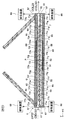
図2は加熱処理ユニット(HT)28(加熱処理装置)を示す平面方向の断面図であり、図3はその側面方向の断面図である。
Next, the heat treatment unit (HT) 28 will be described in detail. The heat treatment unit (HT) 31 has the same structure as the heat treatment unit (HT) 28.
2 is a cross-sectional view in the plane direction showing the heat treatment unit (HT) 28 (heat treatment apparatus), and FIG. 3 is a cross-sectional view in the side surface direction.
加熱処理ユニット(HT)28は、基板GをX方向一方側に向かって搬送するコロ搬送機構5と、コロ搬送機構5を囲繞または収納するように設けられたケーシング6と、ケーシング6内でコロ搬送機構5によってコロ搬送されている基板Gを加熱する加熱機構7とを具備している。
The heat treatment unit (HT) 28 includes a
コロ搬送機構5は、Y方向に延びる略円柱状の回転可能なコロ部材50をX方向に間隔をあけて複数有している。コロ部材50はそれぞれ、回転軸51が図示しないモーター等の駆動源に直接的または間接的に接続され、駆動源の駆動によって回転し、これにより、基板Gが複数のコロ部材50上をX方向一方側に向かって搬送される。また、コロ部材50はそれぞれ、基板Gの全幅(Y方向)にわたって接する形状を有しており、加熱機構7によって加熱された基板Gの熱が伝達しにくいように、外周面部52が樹脂等の熱伝導率の低い材料で形成され、回転軸51がアルミニウム、ステンレス、セラミック等の高強度ながらも熱伝導率の比較的低い材料で形成されている。コロ搬送機構5は、その搬送路または搬送面が搬送ラインA(加熱処理ユニット(HT)31においては搬送ラインB)の一部を構成している。
The
ケーシング6は、薄型の箱状に形成されて基板Gを略水平状態で収容可能であり、X方向に対向する側壁部にそれぞれ、搬送ラインA(加熱処理ユニット(HT)31では搬送ラインB)上の基板Gが通過可能なY方向に延びるスリット状の搬入口61および搬出口62を有している。コロ搬送機構5のコロ部材50はそれぞれ、回転軸51がケーシング6のY方向に対向する側壁部に設けられた軸受け60に回転可能に支持されてケーシング6内に配置されている。
The
ケーシング6の壁部、ここでは上壁部、底壁部およびY方向に対向する側壁部は、互いに空間をあけて設けられた内壁63および外壁64を備えた二重壁構造を有しており、内壁63および外壁64の間の空間65がケーシング6内外を断熱する空気断熱層として機能する。なお、外壁64の内側面にも、ケーシング6内外を断熱するための断熱材66が設けられている。
The wall portion of the
加熱機構7は、コロ搬送機構5による基板Gの搬送路に沿ってケーシング6内に設けられた第1および第2の面状ヒーター71(71a〜71r)、72(72a〜72r)を備えており、第1および第2の面状ヒーター71、72はそれぞれ、コロ搬送機構5によって搬送される基板に近接するように、コロ搬送機構5によって搬送される基板Gの裏面(下面)側および表面(上面)側に設けられている。これにより、ケーシング6の薄型化が図られている。
The
第1の面状ヒーター71は、Y方向に延びる短冊状に形成され、コロ部材50同士の間にそれぞれ設けられてX方向に複数(X方向上流側から順に71a〜71r)配列されている。これにより、ケーシング6のさらなる薄型化が図られている。第1の面状ヒーター71は、例えば、ケーシング6のY方向に対向する側壁部に取り付けられて支持されている。第2の面状ヒーター72は、Y方向に延びる短冊状に形成され、第1の面状ヒーター71の配列ピッチと対応するようにX方向に複数(X方向上流側から順に72a〜72r)配列されている。第2の面状ヒーター72は、ケーシング6に上壁部に取り付けられて支持されている。第1の面状ヒーター71とコロ搬送機構5によって搬送される基板Gの搬送経路との間隔と、第2の面状ヒーター72とコロ搬送機構5によって搬送される基板Gの搬送経路との間隔とは等しくなっている。
The first
本実施形態では、基板Gを加熱するための第1および第2の面状ヒーター71、72を等しいピッチでX方向に複数配列したことにより、第1の面状ヒーター71同士(または第2の面状ヒーター72同士)の間の位置(例えば図3の符号P位置)でケーシング6をX方向に複数分割可能に構成することができる。これにより、基板Gが大型化しても加熱処理装置28自体の運搬が容易である。
In the present embodiment, a plurality of first and second
さらに、本実施形態では、基板Gを加熱するための第2の面状ヒーター72をX方向に複数配列したことにより、第2の面状ヒーター72同士の間の位置(例えば図3の符号P位置)で、ケーシング6の上壁部を観音扉状に開閉可能に構成することができる(図3の仮想線参照)。これにより、ケーシング6内のコロ搬送機構5や加熱機構7のメンテナンスを容易に行うことができる。
Furthermore, in this embodiment, by arranging a plurality of second
第1および第2の面状ヒーター71、72はそれぞれ、図4に示すように(図4は加熱処理装置28を構成する第1および第2の面状ヒーター71、72の概略平面図)、マイカ板に発熱体を設けて構成された複数、例えば4枚のマイカヒーター73(73a、73b、73c、73d)と、これらの複数のマイカヒーター73がY方向に配列されるように取り付けられた短冊状の伝熱体74とを有している。
As shown in FIG. 4, each of the first and second
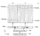
複数の第1および第2の面状ヒーター71a〜71r、72a〜72rは、図5に示すように(図5は第1および第2の面状ヒーター71、72の制御系を示す概念図)、X方向に区分けされたX方向上流側グループの第1および第2の面状ヒーター71a〜71g、72a〜72g(のマイカヒーター73)とX方向下流側グループの第1および第2の面状ヒーター71h〜71r、72h〜72r(のマイカヒーター73)とがそれぞれ、異なるヒーター電源105a、105bに接続されている。X方向上流側グループの第1および第2の面状ヒーター71a〜71g、72a〜72gおよびX方向下流側グループの第1および第2の面状ヒーター71h〜71r、72h〜72rにはそれぞれ、図示しない温度センサーが設けられ、ヒーター電源105a、105bはそれぞれ、温度センサーの検出信号およびプロセスコントローラ101からの指令を受けたヒーターコントローラ(制御部)104によって制御される。すなわち、X方向上流側グループの第1および第2の面状ヒーター71a〜71g、72a〜72gからなる領域SとX方向下流側グループの第1および第2の面状ヒーター71h〜71r、72h〜72rからなる領域Tとは、ヒーターコントローラ104によって別個に温度制御されるように構成されている。なお、領域Sと領域Tとを同じ電源に接続し、この電源における領域Sの出力と領域Tの出力とを変えるように構成してもよい。
The plurality of first and second
ケーシング6のX方向両端部の例えば上壁部および底壁部にはそれぞれ排気口67が設けられており、排気口67には排気装置68が接続されている。そして、排気装置68が作動することにより、排気口67を介してケーシング6内の排気が行われるように構成されている。排気口67および排気装置68は、ケーシング6内が排気する排気機構を構成している。排気口67は、例えば、Y方向に複数形成されていてもよく、Y方向に延びる長孔状に形成されていてもよい。排気機構をケーシング6のX方向両端部にそれぞれ設けることにより、搬入口61および搬出口62にエアカーテンが形成され、外部の塵埃等が搬入口61および搬出口62からケーシング6内に侵入してしまうことが抑止される。なお、排気口67は側壁部に形成されていてもよく、この場合には、X方向に複数、あるいはX方向に延びる長孔状に形成されていてもよい。
一方、ケーシング6のX方向中央部の例えば上壁部および底壁部には、ケーシング内に吸気を行う吸気機構としての吸気口69が設けられている。吸気口69は、例えば、Y方向に複数形成されていてもよく、Y方向に延びる長孔状に形成されていてもよい。排気口67とは対照的に吸気口69をケーシング6のX方向中央部に設けることにより、ケーシング6内の雰囲気の滞留を確実に防止することができるため、加熱機構7による熱をケーシング6内に効果的に拡散させるとともに、加熱処理の際に発生する、レジスト膜に含まれる昇華物のケーシング6内への付着を防止することができる。なお、吸気口69は側壁部に形成されていてもよく、この場合には、X方向に複数、あるいはX方向に延びる長孔状に形成されていてもよい。また、吸気口69に吸気装置(図示せず)を接続し、この吸気装置の作動により、熱せられた空気がケーシング6内に導入されるように構成してもよい。
On the other hand, for example, an upper wall portion and a bottom wall portion of the central portion in the X direction of the
次に、上述の通り構成された加熱処理ユニット(HT)28での基板Gの加熱処理について説明する。 Next, the heat treatment of the substrate G in the heat treatment unit (HT) 28 configured as described above will be described.
加熱処理ユニット(HT)28では、減圧乾燥ユニット(DP)27側(加熱処理ユニット(HT)31では現像ユニット(DEV)30側)の搬送機構によって搬送された基板Gが、搬入口61を通過すると、コロ搬送機構5に受け渡され、このコロ搬送機構5によって搬送されながら、ヒーターコントローラ104によって温度制御された第1および第2の面状ヒーター71、72によりケーシング6内で加熱される。したがって、基板の搬送および加熱が並行して行われるため、処理時間の短縮化が図られる。基板Gは、第1および第2の面状ヒーター71、72によって両面側から加熱されるため、反りが生じるといったことが抑止される。コロ搬送機構5によって搬送された基板Gが、搬出口62を通過すると、冷却ユニット(COL)29側(加熱処理ユニット(HT)31では冷却ユニット(COL)32側)の搬送機構に受け渡され、この平流し式の搬送機構によって搬送されることとなる。したがって、加熱処理時および加熱処理前後の基板Gの搬送がコロ搬送機構5等による所謂平流し式のみなので、基板Gを安全に搬送することができる。
In the heat treatment unit (HT) 28, the substrate G transported by the transport mechanism on the reduced pressure drying unit (DP) 27 side (on the heat treatment unit (HT) 31 on the development unit (DEV) 30 side) passes through the
加熱処理に際しては、X方向上流側グループの第1および第2の面状ヒーター71a〜71g、72a〜72gとX方向下流側グループの第1および第2の面状ヒーター71h〜71r、72h〜72rとがそれぞれ、異なるヒーター電源105a、105bに接続されているため、X方向上流側グループの第1および第2の面状ヒーター71a〜71g、72a〜72gからなる領域SとX方向下流側グループの第1および第2の面状ヒーター71h〜71r、72h〜72rからなる領域Tとを異なる温度に設定することができる。基板Gを所定の温度、例えば130℃程度に加熱する場合に、領域Tを所定の温度の略等しい、または所定の温度よりもやや高い温度、例えば140〜150℃程度に設定し、領域Sを領域Tの温度よりも高い温度、例えば170〜180℃程度に設定すれば、図6に示すように(図6は加熱処理ユニット(HT)28での基板Gの加熱処理を説明するための図)、コロ搬送機構5によって搬送されている基板Gを、領域Sにおいて加熱して(図6(a)参照)、所定の温度近傍まで急速に昇温させた後、領域Tにおいて加熱して(図6(b)参照)、所定の温度に保温するといったことができ、加熱処理時間の短縮化を図ることが可能となる。
In the heat treatment, the first and second
また、第1の面状ヒーター71の配列ピッチと第2の面状ヒーター72の配列ピッチとが等しいため、上下に対応する第1および第2の面状ヒーター71、72を等しい加熱温度に設定することにより、基板Gの反りの発生を確実に防止することが可能となる。
Further, since the arrangement pitch of the first
次に、第1および第2の面状ヒーター71、72の制御系の他の例について説明する。
図7は第1および第2の面状ヒーター71、72の制御系の他の例を示す概念図である。
Next, another example of the control system for the first and second
FIG. 7 is a conceptual diagram showing another example of the control system for the first and second
複数の第1および第2の面状ヒーター71a〜71r、72a〜72rを、X方向に区分けされたグループごとに温度制御可能に構成するとともに、各グループを、マイカヒーター73によってY方向に複数に区分けされた領域ごとに温度制御可能に構成してもよい。例えば、第1および第2の面状ヒーター71a〜71c、72a〜72cのY方向両側部のマイカヒーター73a、73dを有する領域Hと、第1および第2の面状ヒーター71a〜71c、72a〜72cのY方向中央部のマイカヒーター73b、73cを有する領域Iと、第1および第2の面状ヒーター71d〜71g、72d〜72gのY方向両側部のマイカヒーター73a、73dを有する領域Jと、第1および第2の面状ヒーター71d〜71g、72d〜72gのY方向中央部のマイカヒーター73b、73cを有するKと、第1および第2の面状ヒーター71h〜71o、72h〜72oのY方向両側部のマイカヒーター73a、73dを有するLと、第1および第2の面状ヒーター71h〜71o、72h〜72oのY方向中央部のマイカヒーター73b、73cを有するMと、第1および第2の面状ヒーター71p〜71r、72p〜72rのY方向両側部のマイカヒーター73a、73dを有するNと、第1および第2の面状ヒーター71p〜71r、72p〜72rのY方向中央部のマイカヒーター73b、73cを有する領域Oとをそれぞれ、異なるヒーター電源105c〜jに接続し、ヒーター電源105c〜jをそれぞれ、温度センサーの検出信号およびプロセスコントローラ101からの指令を受けたヒーターコントローラ104によって制御させてもよい。このような構成により、複数の第1および第2の面状ヒーター71a〜71r、72a〜72rからなるヒーター群をより細かく制御することができる。なお、領域H〜Oを同じ電源に接続し、この電源における領域H〜Oの出力を変えるように構成してもよく、図5に示した制御系と併用して、領域H〜Kおよび領域L〜Oをそれぞれ同じ電源に接続し、これらの電源における領域H〜Kおよび領域L〜Oの出力をそれぞれ変えるように構成してもよい。
The plurality of first and second
この場合に、ケーシング6の側壁部や排気機構等による熱損失を考慮して、領域Sにおいては、領域Kよりも領域I、Jの温度を高く設定し、かつ、領域I、Jよりも領域Hの温度を高く設定するとともに、領域Tにおいては、領域Mよりも領域O、Lの温度を高く設定し、かつ、領域O、Lよりも領域Nの温度を高く設定すれば、加熱処理時間の短縮化を図ることができるとともに、領域Sおよび領域Tにおいて、ケーシング6内の基板Gの全面を均等な温度に加熱することでき、加熱処理の品質を向上させることが可能となる。
In this case, in consideration of heat loss due to the side wall portion of the
ヒーターは通常、被加熱物に対してある程度の距離をあけて設けると、被加熱物を均等に加熱しやすくなる代わりに加熱効率が低くなるが、本実施形態では、複数の第1および第2の面状ヒーター71a〜71r、72a〜72rからなるヒーター群が区分けされた領域ごとに温度制御可能であるため、第1および第2の面状ヒーター71、72をコロ搬送機構5によって搬送される基板Gと近接するように設けても、基板G全体を均等に加熱することが可能となる。コロ搬送機構5によって搬送される基板Gが第1および第2の面状ヒーター71、72と接触しないように、かつ、第1および第2の面状ヒーター71、72の加熱効率を低下させないように、コロ搬送機構5によって搬送される基板Gの搬送経路と第1の面状ヒーター71および第2の面状ヒーター72との間隔はそれぞれ、5〜30mmとすることが好ましい。
Normally, when the heater is provided at a certain distance from the object to be heated, the heating efficiency is lowered instead of easily heating the object to be heated. In the present embodiment, a plurality of first and second elements are used. Since the temperature control is possible for each area where the heater group composed of the
なお、第1および第2の面状ヒーター71a〜71r、72a〜72rをそれぞれ、異なるヒーター電源に接続して、ヒーターコントローラ104によって個別に温度制御可能に構成してもよく、さらには、第1および第2の面状ヒーター71a〜71r、72a〜72rのマイカヒーター73a〜73dをそれぞれ、異なるヒーター電源に接続して、ヒーターコントローラ104によって個別に温度制御可能に構成してもよい。
Note that the first and second
本実施形態においては、複数の第1および第2の面状ヒーター71a〜71r、72a〜72rが個別またはX方向に区分けされたグループごとに温度制御され、るため、複数の第1および第2の面状ヒーター71a〜71r、72a〜72rからなるヒーター群は、用途に応じた所定の温度プロファイルを形成することが可能となる。
In the present embodiment, the plurality of first and second
本発明によれば、FPD用のガラス基板のように特に基板が大型の場合に好適であるが、ガラス基板に限らず、半導体ウエハなどの他の基板の加熱処理にも広く適用することができる。 According to the present invention, it is suitable particularly when the substrate is large, such as an FPD glass substrate, but is not limited to the glass substrate and can be widely applied to heat treatment of other substrates such as a semiconductor wafer. .
28、31…加熱処理ユニット(加熱処理装置)
5…コロ搬送機構
6…ケーシング
50…コロ部材
52…外周面部
63…内壁
64…外壁
65…空間
71(71a〜71r)…第1の面状ヒーター
72(72a〜72r)…第2の面状ヒーター
G…基板
28, 31 ... Heat treatment unit (heat treatment apparatus)
DESCRIPTION OF
Claims (9)
基板を一方向に搬送する搬送路と、
前記搬送路を囲繞するように設けられたケーシングと、
前記搬送路に沿って前記ケーシング内に、前記搬送路を搬送される基板に近接するように基板の両面側にそれぞれ設けられた第1および第2の面状ヒーターと
を具備することを特徴とする加熱処理装置。 A heat treatment apparatus for performing heat treatment on a substrate,
A transport path for transporting the substrate in one direction;
A casing provided so as to surround the conveyance path;
The first and second planar heaters respectively provided on both sides of the substrate so as to be close to the substrate conveyed along the conveyance path in the casing along the conveyance path. Heat treatment equipment.
前記第1の面状ヒーターは、前記コロ部材同士の間にそれぞれ設けられて搬送方向に複数配列されていることを特徴とする請求項1に記載の加熱処理装置。 The transport path rolls the substrate by rotating a plurality of roller members provided at intervals in one direction,
2. The heat treatment apparatus according to claim 1, wherein a plurality of the first planar heaters are provided between the roller members and arranged in the transport direction.
前記複数の第1および第2の面状ヒーターは、個別または搬送方向に区分けされたグループごとに温度制御可能であることを特徴とする請求項2に記載の加熱処理装置。 A plurality of the second planar heaters are arranged in the transport direction so as to correspond to the arrangement pitch of the first planar heaters,
The heat treatment apparatus according to claim 2, wherein the plurality of first and second planar heaters can be controlled in temperature individually or for each group divided in the transport direction.
前記ケーシングの前記一壁部は、前記ケーシング内を開閉する扉として機能することを特徴とする請求項3から請求項5のいずれか1項に記載の加熱処理装置。 The second planar heater is attached to one wall portion of the casing,
The heat treatment apparatus according to any one of claims 3 to 5, wherein the one wall portion of the casing functions as a door that opens and closes the inside of the casing.
Priority Applications (4)
| Application Number | Priority Date | Filing Date | Title |
|---|---|---|---|
| JP2005355183A JP4531690B2 (en) | 2005-12-08 | 2005-12-08 | Heat treatment device |
| TW095145644A TWI339872B (en) | 2005-12-08 | 2006-12-07 | Heat treatment unit |
| KR1020060123948A KR101269748B1 (en) | 2005-12-08 | 2006-12-07 | Heat treatment unit |
| CNB2006101656028A CN100474507C (en) | 2005-12-08 | 2006-12-08 | Heat treatment unit |
Applications Claiming Priority (1)
| Application Number | Priority Date | Filing Date | Title |
|---|---|---|---|
| JP2005355183A JP4531690B2 (en) | 2005-12-08 | 2005-12-08 | Heat treatment device |
Publications (2)
| Publication Number | Publication Date |
|---|---|
| JP2007158253A true JP2007158253A (en) | 2007-06-21 |
| JP4531690B2 JP4531690B2 (en) | 2010-08-25 |
Family
ID=38130875
Family Applications (1)
| Application Number | Title | Priority Date | Filing Date |
|---|---|---|---|
| JP2005355183A Active JP4531690B2 (en) | 2005-12-08 | 2005-12-08 | Heat treatment device |
Country Status (4)
| Country | Link |
|---|---|
| JP (1) | JP4531690B2 (en) |
| KR (1) | KR101269748B1 (en) |
| CN (1) | CN100474507C (en) |
| TW (1) | TWI339872B (en) |
Cited By (11)
| Publication number | Priority date | Publication date | Assignee | Title |
|---|---|---|---|---|
| JP2011066318A (en) * | 2009-09-18 | 2011-03-31 | Tokyo Electron Ltd | Heat processing apparatus |
| JP2011216572A (en) * | 2010-03-31 | 2011-10-27 | Dainippon Screen Mfg Co Ltd | Substrate processing apparatus |
| KR20120002428A (en) | 2010-06-30 | 2012-01-05 | 도쿄엘렉트론가부시키가이샤 | Local site exposure apparatus and local site exposure method and storage medium |
| KR20120071347A (en) | 2010-12-22 | 2012-07-02 | 도쿄엘렉트론가부시키가이샤 | Local exposure method and local exposure apparatus |
| JP2012182308A (en) * | 2011-03-01 | 2012-09-20 | Tokyo Electron Ltd | Levitation coating apparatus |
| KR20120105374A (en) | 2011-03-15 | 2012-09-25 | 도쿄엘렉트론가부시키가이샤 | Local site exposure method and local site exposure apparatus |
| JP2013061081A (en) * | 2011-09-12 | 2013-04-04 | Dainippon Screen Mfg Co Ltd | Heat treatment apparatus |
| JP2020035884A (en) * | 2018-08-30 | 2020-03-05 | 東京エレクトロン株式会社 | Substrate processing apparatus and substrate processing method |
| JP2020035935A (en) * | 2018-08-30 | 2020-03-05 | 東京エレクトロン株式会社 | Substrate processing apparatus and substrate processing method |
| KR20200081257A (en) | 2018-12-27 | 2020-07-07 | 도쿄엘렉트론가부시키가이샤 | Substrate processing apparatus and substrate processing method |
| KR20200081256A (en) | 2018-12-27 | 2020-07-07 | 도쿄엘렉트론가부시키가이샤 | Substrate processing apparatus and substrate processing method |
Families Citing this family (5)
| Publication number | Priority date | Publication date | Assignee | Title |
|---|---|---|---|---|
| KR101055862B1 (en) * | 2009-03-23 | 2011-08-09 | 주식회사 테라세미콘 | Inline heat treatment equipment |
| JP5226037B2 (en) * | 2010-06-04 | 2013-07-03 | 東京エレクトロン株式会社 | Heat treatment apparatus and heat treatment method |
| JP7265314B2 (en) * | 2017-03-03 | 2023-04-26 | 株式会社Screenホールディングス | Heat treatment method and heat treatment apparatus |
| US11476167B2 (en) | 2017-03-03 | 2022-10-18 | SCREEN Holdings Co., Ltd. | Heat treatment method and heat treatment apparatus of light irradiation type |
| KR102220853B1 (en) * | 2019-05-27 | 2021-02-26 | 주식회사 선코리아 | Thermal processing apparatus |
Citations (9)
| Publication number | Priority date | Publication date | Assignee | Title |
|---|---|---|---|---|
| JPS62252989A (en) * | 1986-04-25 | 1987-11-04 | 日本電気株式会社 | Manufacture of printed circuit board |
| JPH0193121A (en) * | 1987-10-05 | 1989-04-12 | Kawasaki Steel Corp | Semiconductor wafer baking device |
| JPH0270426A (en) * | 1988-09-06 | 1990-03-09 | Kawasaki Steel Corp | Composite steel plate having vibration suppressing property |
| JPH04243119A (en) * | 1991-01-17 | 1992-08-31 | Sharp Corp | Resist heating apparatus |
| JPH0531223U (en) * | 1991-09-30 | 1993-04-23 | 日本電気株式会社 | LCD Display Active Device Manufacturing Equipment |
| JPH0845817A (en) * | 1994-07-28 | 1996-02-16 | Fujitsu Ltd | Baking device |
| JPH0953881A (en) * | 1995-08-11 | 1997-02-25 | Fuji Photo Film Co Ltd | Baking device of hard board |
| JPH09310198A (en) * | 1996-05-20 | 1997-12-02 | Dainippon Printing Co Ltd | Electrodeposition resist drying device |
| JPH1147668A (en) * | 1997-06-06 | 1999-02-23 | Kansai Denshi Kk | Substrate dryer |
Family Cites Families (1)
| Publication number | Priority date | Publication date | Assignee | Title |
|---|---|---|---|---|
| JP2005123284A (en) * | 2003-10-15 | 2005-05-12 | Renesas Technology Corp | Semiconductor manufacturing device |
-
2005
- 2005-12-08 JP JP2005355183A patent/JP4531690B2/en active Active
-
2006
- 2006-12-07 TW TW095145644A patent/TWI339872B/en not_active IP Right Cessation
- 2006-12-07 KR KR1020060123948A patent/KR101269748B1/en active IP Right Grant
- 2006-12-08 CN CNB2006101656028A patent/CN100474507C/en not_active Expired - Fee Related
Patent Citations (9)
| Publication number | Priority date | Publication date | Assignee | Title |
|---|---|---|---|---|
| JPS62252989A (en) * | 1986-04-25 | 1987-11-04 | 日本電気株式会社 | Manufacture of printed circuit board |
| JPH0193121A (en) * | 1987-10-05 | 1989-04-12 | Kawasaki Steel Corp | Semiconductor wafer baking device |
| JPH0270426A (en) * | 1988-09-06 | 1990-03-09 | Kawasaki Steel Corp | Composite steel plate having vibration suppressing property |
| JPH04243119A (en) * | 1991-01-17 | 1992-08-31 | Sharp Corp | Resist heating apparatus |
| JPH0531223U (en) * | 1991-09-30 | 1993-04-23 | 日本電気株式会社 | LCD Display Active Device Manufacturing Equipment |
| JPH0845817A (en) * | 1994-07-28 | 1996-02-16 | Fujitsu Ltd | Baking device |
| JPH0953881A (en) * | 1995-08-11 | 1997-02-25 | Fuji Photo Film Co Ltd | Baking device of hard board |
| JPH09310198A (en) * | 1996-05-20 | 1997-12-02 | Dainippon Printing Co Ltd | Electrodeposition resist drying device |
| JPH1147668A (en) * | 1997-06-06 | 1999-02-23 | Kansai Denshi Kk | Substrate dryer |
Cited By (18)
| Publication number | Priority date | Publication date | Assignee | Title |
|---|---|---|---|---|
| JP2011066318A (en) * | 2009-09-18 | 2011-03-31 | Tokyo Electron Ltd | Heat processing apparatus |
| JP2011216572A (en) * | 2010-03-31 | 2011-10-27 | Dainippon Screen Mfg Co Ltd | Substrate processing apparatus |
| KR20120002428A (en) | 2010-06-30 | 2012-01-05 | 도쿄엘렉트론가부시키가이샤 | Local site exposure apparatus and local site exposure method and storage medium |
| US9146481B2 (en) | 2010-06-30 | 2015-09-29 | Tokyo Electron Limited | Local exposure apparatus, local exposure method and storage medium |
| US8691481B2 (en) | 2010-12-22 | 2014-04-08 | Tokyo Electron Limited | Local exposure method and local exposure apparatus |
| KR20120071347A (en) | 2010-12-22 | 2012-07-02 | 도쿄엘렉트론가부시키가이샤 | Local exposure method and local exposure apparatus |
| JP2012182308A (en) * | 2011-03-01 | 2012-09-20 | Tokyo Electron Ltd | Levitation coating apparatus |
| KR20120105374A (en) | 2011-03-15 | 2012-09-25 | 도쿄엘렉트론가부시키가이샤 | Local site exposure method and local site exposure apparatus |
| JP2013061081A (en) * | 2011-09-12 | 2013-04-04 | Dainippon Screen Mfg Co Ltd | Heat treatment apparatus |
| JP2020035884A (en) * | 2018-08-30 | 2020-03-05 | 東京エレクトロン株式会社 | Substrate processing apparatus and substrate processing method |
| JP2020035935A (en) * | 2018-08-30 | 2020-03-05 | 東京エレクトロン株式会社 | Substrate processing apparatus and substrate processing method |
| KR20200026085A (en) | 2018-08-30 | 2020-03-10 | 도쿄엘렉트론가부시키가이샤 | Substate processing apparatus and substate processing method |
| KR20200026084A (en) | 2018-08-30 | 2020-03-10 | 도쿄엘렉트론가부시키가이샤 | Substate processing apparatus and substate processing method |
| JP7232596B2 (en) | 2018-08-30 | 2023-03-03 | 東京エレクトロン株式会社 | SUBSTRATE PROCESSING APPARATUS AND SUBSTRATE PROCESSING METHOD |
| JP7232593B2 (en) | 2018-08-30 | 2023-03-03 | 東京エレクトロン株式会社 | SUBSTRATE PROCESSING APPARATUS AND SUBSTRATE PROCESSING METHOD |
| KR20200081257A (en) | 2018-12-27 | 2020-07-07 | 도쿄엘렉트론가부시키가이샤 | Substrate processing apparatus and substrate processing method |
| CN111383975A (en) * | 2018-12-27 | 2020-07-07 | 东京毅力科创株式会社 | Substrate processing apparatus and substrate processing method |
| KR20200081256A (en) | 2018-12-27 | 2020-07-07 | 도쿄엘렉트론가부시키가이샤 | Substrate processing apparatus and substrate processing method |
Also Published As
| Publication number | Publication date |
|---|---|
| KR101269748B1 (en) | 2013-05-30 |
| CN100474507C (en) | 2009-04-01 |
| CN1979765A (en) | 2007-06-13 |
| KR20070061418A (en) | 2007-06-13 |
| JP4531690B2 (en) | 2010-08-25 |
| TWI339872B (en) | 2011-04-01 |
| TW200737393A (en) | 2007-10-01 |
Similar Documents
| Publication | Publication Date | Title |
|---|---|---|
| JP4531690B2 (en) | Heat treatment device | |
| JP4672538B2 (en) | Heat treatment device | |
| JP4542577B2 (en) | Normal pressure drying apparatus, substrate processing apparatus, and substrate processing method | |
| JP4537324B2 (en) | Substrate cooling device, substrate cooling method, control program, computer-readable storage medium | |
| JP4341978B2 (en) | Substrate processing equipment | |
| JP5377463B2 (en) | Heat treatment device | |
| JP4384686B2 (en) | Normal pressure drying apparatus, substrate processing apparatus, and substrate processing method | |
| JP4537323B2 (en) | Substrate cooling device | |
| JP4319175B2 (en) | Vacuum dryer | |
| KR20080060165A (en) | Substrate processing apparatus | |
| JP4407971B2 (en) | Substrate processing equipment | |
| JP2010056359A (en) | Substrate transfer device | |
| TWI797325B (en) | Substrate processing apparatus and substrate processing method | |
| JP3576826B2 (en) | Heat treatment apparatus and heat treatment method | |
| JP4472647B2 (en) | Heat treatment apparatus, heat treatment method, and computer-readable storage medium | |
| JP4015015B2 (en) | Heat treatment equipment | |
| JP3966884B2 (en) | Substrate processing apparatus, substrate processing method, and substrate manufacturing method | |
| JP2008166820A (en) | Apparatus and method for processing substrate, method for manufacturing substrate, and electronic instrument | |
| JP2008109158A (en) | Substrate treatment apparatus, substrate treatment method, substrate producing method and electronic device | |
| JP2008124502A (en) | Substrate treatment equipment, method for treating substrate, method for manufacturing substrate, and electronic instrument | |
| JP2005142590A (en) | Substrate processing device and method, and method for manufacturing substrate | |
| JP2011121775A (en) | Substrate processing device, substrate processing method, and recording medium recording program for executing the substrate processing method |
Legal Events
| Date | Code | Title | Description |
|---|---|---|---|
| A621 | Written request for application examination |
Free format text: JAPANESE INTERMEDIATE CODE: A621 Effective date: 20070903 |
|
| A131 | Notification of reasons for refusal |
Free format text: JAPANESE INTERMEDIATE CODE: A131 Effective date: 20091222 |
|
| A521 | Request for written amendment filed |
Free format text: JAPANESE INTERMEDIATE CODE: A523 Effective date: 20100219 |
|
| TRDD | Decision of grant or rejection written | ||
| A01 | Written decision to grant a patent or to grant a registration (utility model) |
Free format text: JAPANESE INTERMEDIATE CODE: A01 Effective date: 20100608 |
|
| A01 | Written decision to grant a patent or to grant a registration (utility model) |
Free format text: JAPANESE INTERMEDIATE CODE: A01 |
|
| A61 | First payment of annual fees (during grant procedure) |
Free format text: JAPANESE INTERMEDIATE CODE: A61 Effective date: 20100609 |
|
| R150 | Certificate of patent or registration of utility model |
Ref document number: 4531690 Country of ref document: JP Free format text: JAPANESE INTERMEDIATE CODE: R150 Free format text: JAPANESE INTERMEDIATE CODE: R150 |
|
| FPAY | Renewal fee payment (event date is renewal date of database) |
Free format text: PAYMENT UNTIL: 20130618 Year of fee payment: 3 |
|
| R250 | Receipt of annual fees |
Free format text: JAPANESE INTERMEDIATE CODE: R250 |
|
| R250 | Receipt of annual fees |
Free format text: JAPANESE INTERMEDIATE CODE: R250 |
|
| R250 | Receipt of annual fees |
Free format text: JAPANESE INTERMEDIATE CODE: R250 |
|
| R250 | Receipt of annual fees |
Free format text: JAPANESE INTERMEDIATE CODE: R250 |
|
| R250 | Receipt of annual fees |
Free format text: JAPANESE INTERMEDIATE CODE: R250 |
|
| R250 | Receipt of annual fees |
Free format text: JAPANESE INTERMEDIATE CODE: R250 |
|
| R250 | Receipt of annual fees |
Free format text: JAPANESE INTERMEDIATE CODE: R250 |