JP2006507683A - A transistor including a p-type buried layer under a source region and a manufacturing method thereof. - Google Patents
A transistor including a p-type buried layer under a source region and a manufacturing method thereof. Download PDFInfo
- Publication number
- JP2006507683A JP2006507683A JP2004555310A JP2004555310A JP2006507683A JP 2006507683 A JP2006507683 A JP 2006507683A JP 2004555310 A JP2004555310 A JP 2004555310A JP 2004555310 A JP2004555310 A JP 2004555310A JP 2006507683 A JP2006507683 A JP 2006507683A
- Authority
- JP
- Japan
- Prior art keywords
- conductivity type
- forming
- field effect
- effect transistor
- source
- Prior art date
- Legal status (The legal status is an assumption and is not a legal conclusion. Google has not performed a legal analysis and makes no representation as to the accuracy of the status listed.)
- Pending
Links
- 238000004519 manufacturing process Methods 0.000 title claims description 54
- 239000004065 semiconductor Substances 0.000 claims abstract description 113
- 230000005669 field effect Effects 0.000 claims abstract description 103
- 108091006146 Channels Proteins 0.000 claims description 175
- HBMJWWWQQXIZIP-UHFFFAOYSA-N silicon carbide Chemical compound [Si+]#[C-] HBMJWWWQQXIZIP-UHFFFAOYSA-N 0.000 claims description 150
- 229910010271 silicon carbide Inorganic materials 0.000 claims description 140
- 229910052751 metal Inorganic materials 0.000 claims description 108
- 239000002184 metal Substances 0.000 claims description 108
- 239000000758 substrate Substances 0.000 claims description 91
- 238000000034 method Methods 0.000 claims description 31
- PXHVJJICTQNCMI-UHFFFAOYSA-N Nickel Chemical compound [Ni] PXHVJJICTQNCMI-UHFFFAOYSA-N 0.000 claims description 26
- JBRZTFJDHDCESZ-UHFFFAOYSA-N AsGa Chemical compound [As]#[Ga] JBRZTFJDHDCESZ-UHFFFAOYSA-N 0.000 claims description 24
- 238000005530 etching Methods 0.000 claims description 23
- JMASRVWKEDWRBT-UHFFFAOYSA-N Gallium nitride Chemical compound [Ga]#N JMASRVWKEDWRBT-UHFFFAOYSA-N 0.000 claims description 22
- BASFCYQUMIYNBI-UHFFFAOYSA-N platinum Chemical compound [Pt] BASFCYQUMIYNBI-UHFFFAOYSA-N 0.000 claims description 19
- 239000002019 doping agent Substances 0.000 claims description 18
- 238000002513 implantation Methods 0.000 claims description 17
- 239000000463 material Substances 0.000 claims description 17
- 229910001218 Gallium arsenide Inorganic materials 0.000 claims description 16
- 229910002601 GaN Inorganic materials 0.000 claims description 14
- 239000007943 implant Substances 0.000 claims description 14
- 229910052759 nickel Inorganic materials 0.000 claims description 13
- PCHJSUWPFVWCPO-UHFFFAOYSA-N gold Chemical compound [Au] PCHJSUWPFVWCPO-UHFFFAOYSA-N 0.000 claims description 12
- 229910052737 gold Inorganic materials 0.000 claims description 11
- 239000010931 gold Substances 0.000 claims description 11
- 230000005684 electric field Effects 0.000 claims description 10
- 238000000137 annealing Methods 0.000 claims description 9
- 239000011651 chromium Substances 0.000 claims description 9
- 229910052697 platinum Inorganic materials 0.000 claims description 9
- VYZAMTAEIAYCRO-UHFFFAOYSA-N Chromium Chemical compound [Cr] VYZAMTAEIAYCRO-UHFFFAOYSA-N 0.000 claims description 7
- 229910052804 chromium Inorganic materials 0.000 claims description 7
- 238000000151 deposition Methods 0.000 claims description 6
- FTWRSWRBSVXQPI-UHFFFAOYSA-N alumanylidynearsane;gallanylidynearsane Chemical compound [As]#[Al].[As]#[Ga] FTWRSWRBSVXQPI-UHFFFAOYSA-N 0.000 claims description 5
- 230000000694 effects Effects 0.000 claims description 5
- 238000002347 injection Methods 0.000 claims description 5
- 239000007924 injection Substances 0.000 claims description 5
- 230000002093 peripheral effect Effects 0.000 claims description 4
- 102000004129 N-Type Calcium Channels Human genes 0.000 claims description 2
- 108090000699 N-Type Calcium Channels Proteins 0.000 claims description 2
- RNQKDQAVIXDKAG-UHFFFAOYSA-N aluminum gallium Chemical compound [Al].[Ga] RNQKDQAVIXDKAG-UHFFFAOYSA-N 0.000 claims description 2
- 230000003213 activating effect Effects 0.000 claims 1
- 230000000149 penetrating effect Effects 0.000 claims 1
- 230000015556 catabolic process Effects 0.000 description 16
- 230000008569 process Effects 0.000 description 8
- 239000012212 insulator Substances 0.000 description 6
- IJGRMHOSHXDMSA-UHFFFAOYSA-N Atomic nitrogen Chemical compound N#N IJGRMHOSHXDMSA-UHFFFAOYSA-N 0.000 description 4
- 229910001385 heavy metal Inorganic materials 0.000 description 4
- 150000002500 ions Chemical class 0.000 description 4
- 238000002955 isolation Methods 0.000 description 4
- 230000007704 transition Effects 0.000 description 4
- XUIMIQQOPSSXEZ-UHFFFAOYSA-N Silicon Chemical compound [Si] XUIMIQQOPSSXEZ-UHFFFAOYSA-N 0.000 description 3
- 229910052782 aluminium Inorganic materials 0.000 description 3
- XAGFODPZIPBFFR-UHFFFAOYSA-N aluminium Chemical compound [Al] XAGFODPZIPBFFR-UHFFFAOYSA-N 0.000 description 3
- 230000015572 biosynthetic process Effects 0.000 description 3
- 150000001875 compounds Chemical class 0.000 description 3
- 239000013078 crystal Substances 0.000 description 3
- 230000007547 defect Effects 0.000 description 3
- 238000001312 dry etching Methods 0.000 description 3
- 229910052710 silicon Inorganic materials 0.000 description 3
- 239000010703 silicon Substances 0.000 description 3
- 229910052720 vanadium Inorganic materials 0.000 description 3
- LEONUFNNVUYDNQ-UHFFFAOYSA-N vanadium atom Chemical compound [V] LEONUFNNVUYDNQ-UHFFFAOYSA-N 0.000 description 3
- -1 AlGaN Chemical compound 0.000 description 2
- ZOXJGFHDIHLPTG-UHFFFAOYSA-N Boron Chemical compound [B] ZOXJGFHDIHLPTG-UHFFFAOYSA-N 0.000 description 2
- GYHNNYVSQQEPJS-UHFFFAOYSA-N Gallium Chemical compound [Ga] GYHNNYVSQQEPJS-UHFFFAOYSA-N 0.000 description 2
- 230000008901 benefit Effects 0.000 description 2
- 229910052796 boron Inorganic materials 0.000 description 2
- 239000000969 carrier Substances 0.000 description 2
- 230000007423 decrease Effects 0.000 description 2
- 230000008021 deposition Effects 0.000 description 2
- 229910052733 gallium Inorganic materials 0.000 description 2
- 230000017525 heat dissipation Effects 0.000 description 2
- 238000005468 ion implantation Methods 0.000 description 2
- 150000002739 metals Chemical class 0.000 description 2
- 229910052757 nitrogen Inorganic materials 0.000 description 2
- 230000003071 parasitic effect Effects 0.000 description 2
- 229920006395 saturated elastomer Polymers 0.000 description 2
- 238000001039 wet etching Methods 0.000 description 2
- ZXEYZECDXFPJRJ-UHFFFAOYSA-N $l^{3}-silane;platinum Chemical compound [SiH3].[Pt] ZXEYZECDXFPJRJ-UHFFFAOYSA-N 0.000 description 1
- RYGMFSIKBFXOCR-UHFFFAOYSA-N Copper Chemical compound [Cu] RYGMFSIKBFXOCR-UHFFFAOYSA-N 0.000 description 1
- OAICVXFJPJFONN-UHFFFAOYSA-N Phosphorus Chemical compound [P] OAICVXFJPJFONN-UHFFFAOYSA-N 0.000 description 1
- BQCADISMDOOEFD-UHFFFAOYSA-N Silver Chemical compound [Ag] BQCADISMDOOEFD-UHFFFAOYSA-N 0.000 description 1
- RTAQQCXQSZGOHL-UHFFFAOYSA-N Titanium Chemical compound [Ti] RTAQQCXQSZGOHL-UHFFFAOYSA-N 0.000 description 1
- 238000003763 carbonization Methods 0.000 description 1
- 229910052802 copper Inorganic materials 0.000 description 1
- 239000010949 copper Substances 0.000 description 1
- 230000008878 coupling Effects 0.000 description 1
- 238000010168 coupling process Methods 0.000 description 1
- 238000005859 coupling reaction Methods 0.000 description 1
- 238000010586 diagram Methods 0.000 description 1
- 238000009616 inductively coupled plasma Methods 0.000 description 1
- 238000011835 investigation Methods 0.000 description 1
- 229910044991 metal oxide Inorganic materials 0.000 description 1
- 150000004706 metal oxides Chemical class 0.000 description 1
- 238000004377 microelectronic Methods 0.000 description 1
- 230000003647 oxidation Effects 0.000 description 1
- 238000007254 oxidation reaction Methods 0.000 description 1
- 229910052698 phosphorus Inorganic materials 0.000 description 1
- 239000011574 phosphorus Substances 0.000 description 1
- 238000001020 plasma etching Methods 0.000 description 1
- 229910021339 platinum silicide Inorganic materials 0.000 description 1
- 239000000843 powder Substances 0.000 description 1
- 239000002994 raw material Substances 0.000 description 1
- 230000004044 response Effects 0.000 description 1
- 229910052709 silver Inorganic materials 0.000 description 1
- 239000004332 silver Substances 0.000 description 1
- 239000010936 titanium Substances 0.000 description 1
- 229910052719 titanium Inorganic materials 0.000 description 1
- 238000001771 vacuum deposition Methods 0.000 description 1
Images


Classifications
-
- H—ELECTRICITY
- H01—ELECTRIC ELEMENTS
- H01L—SEMICONDUCTOR DEVICES NOT COVERED BY CLASS H10
- H01L29/00—Semiconductor devices adapted for rectifying, amplifying, oscillating or switching, or capacitors or resistors with at least one potential-jump barrier or surface barrier, e.g. PN junction depletion layer or carrier concentration layer; Details of semiconductor bodies or of electrodes thereof ; Multistep manufacturing processes therefor
- H01L29/66—Types of semiconductor device ; Multistep manufacturing processes therefor
- H01L29/66007—Multistep manufacturing processes
- H01L29/66075—Multistep manufacturing processes of devices having semiconductor bodies comprising group 14 or group 13/15 materials
- H01L29/66227—Multistep manufacturing processes of devices having semiconductor bodies comprising group 14 or group 13/15 materials the devices being controllable only by the electric current supplied or the electric potential applied, to an electrode which does not carry the current to be rectified, amplified or switched, e.g. three-terminal devices
- H01L29/66409—Unipolar field-effect transistors
- H01L29/66848—Unipolar field-effect transistors with a Schottky gate, i.e. MESFET
- H01L29/66856—Unipolar field-effect transistors with a Schottky gate, i.e. MESFET with an active layer made of a group 13/15 material
-
- H—ELECTRICITY
- H01—ELECTRIC ELEMENTS
- H01L—SEMICONDUCTOR DEVICES NOT COVERED BY CLASS H10
- H01L29/00—Semiconductor devices adapted for rectifying, amplifying, oscillating or switching, or capacitors or resistors with at least one potential-jump barrier or surface barrier, e.g. PN junction depletion layer or carrier concentration layer; Details of semiconductor bodies or of electrodes thereof ; Multistep manufacturing processes therefor
- H01L29/66—Types of semiconductor device ; Multistep manufacturing processes therefor
- H01L29/66007—Multistep manufacturing processes
- H01L29/66053—Multistep manufacturing processes of devices having a semiconductor body comprising crystalline silicon carbide
- H01L29/66068—Multistep manufacturing processes of devices having a semiconductor body comprising crystalline silicon carbide the devices being controllable only by the electric current supplied or the electric potential applied, to an electrode which does not carry the current to be rectified, amplified or switched, e.g. three-terminal devices
-
- H—ELECTRICITY
- H01—ELECTRIC ELEMENTS
- H01L—SEMICONDUCTOR DEVICES NOT COVERED BY CLASS H10
- H01L29/00—Semiconductor devices adapted for rectifying, amplifying, oscillating or switching, or capacitors or resistors with at least one potential-jump barrier or surface barrier, e.g. PN junction depletion layer or carrier concentration layer; Details of semiconductor bodies or of electrodes thereof ; Multistep manufacturing processes therefor
- H01L29/66—Types of semiconductor device ; Multistep manufacturing processes therefor
- H01L29/68—Types of semiconductor device ; Multistep manufacturing processes therefor controllable by only the electric current supplied, or only the electric potential applied, to an electrode which does not carry the current to be rectified, amplified or switched
- H01L29/76—Unipolar devices, e.g. field effect transistors
- H01L29/772—Field effect transistors
- H01L29/80—Field effect transistors with field effect produced by a PN or other rectifying junction gate, i.e. potential-jump barrier
- H01L29/812—Field effect transistors with field effect produced by a PN or other rectifying junction gate, i.e. potential-jump barrier with a Schottky gate
- H01L29/8128—Field effect transistors with field effect produced by a PN or other rectifying junction gate, i.e. potential-jump barrier with a Schottky gate with recessed gate
-
- H—ELECTRICITY
- H01—ELECTRIC ELEMENTS
- H01L—SEMICONDUCTOR DEVICES NOT COVERED BY CLASS H10
- H01L29/00—Semiconductor devices adapted for rectifying, amplifying, oscillating or switching, or capacitors or resistors with at least one potential-jump barrier or surface barrier, e.g. PN junction depletion layer or carrier concentration layer; Details of semiconductor bodies or of electrodes thereof ; Multistep manufacturing processes therefor
- H01L29/02—Semiconductor bodies ; Multistep manufacturing processes therefor
- H01L29/12—Semiconductor bodies ; Multistep manufacturing processes therefor characterised by the materials of which they are formed
- H01L29/16—Semiconductor bodies ; Multistep manufacturing processes therefor characterised by the materials of which they are formed including, apart from doping materials or other impurities, only elements of Group IV of the Periodic System
- H01L29/1608—Silicon carbide
-
- H—ELECTRICITY
- H01—ELECTRIC ELEMENTS
- H01L—SEMICONDUCTOR DEVICES NOT COVERED BY CLASS H10
- H01L29/00—Semiconductor devices adapted for rectifying, amplifying, oscillating or switching, or capacitors or resistors with at least one potential-jump barrier or surface barrier, e.g. PN junction depletion layer or carrier concentration layer; Details of semiconductor bodies or of electrodes thereof ; Multistep manufacturing processes therefor
- H01L29/02—Semiconductor bodies ; Multistep manufacturing processes therefor
- H01L29/12—Semiconductor bodies ; Multistep manufacturing processes therefor characterised by the materials of which they are formed
- H01L29/20—Semiconductor bodies ; Multistep manufacturing processes therefor characterised by the materials of which they are formed including, apart from doping materials or other impurities, only AIIIBV compounds
- H01L29/2003—Nitride compounds
Abstract
Description
本発明は、ソース領域の下にp型埋込み層を備えたトランジスタ及びその作製方法に関し、より詳細には、微小電子デバイス、例えば、金属半導体電界効果トランジスタ(MESFET)及びその作製方法に関する。 The present invention relates to a transistor having a p-type buried layer under a source region and a manufacturing method thereof, and more particularly to a microelectronic device such as a metal semiconductor field effect transistor (MESFET) and a manufacturing method thereof.
なお、本発明は、米国海軍省の契約番号第N39997−99−C−3761号の助成契約の少なくとも部分的な助成の基でなされた。米国政府は、本発明に何らかの権利を有することができる。 The present invention was made on the basis of at least partial subsidy of the subsidy contract of the US Navy contract number N39997-99-C-3761. The US government may have some rights in the invention.
無線周波数(500MHz)、S−バンド(3GHz)、及びX−バンド(10GHz)などの高周波で動作しつつ、ハイパワー(>20ワット)の処理能力を必要とする電気回路が、近年より普及してきた。ハイパワーの高周波回路が増加したため、これに対応して、よりハイパワーの負荷の処理能力を維持したまま無線周波数以上で高い信頼性で動作することができるトランジスタの需要が増大してきた。従来は、バイポーラトランジスタ及び金属酸化膜半導体電界効果トランジスタ(MOSFET)がハイパワー用途に使用されてきたが、このようなデバイスのパワー処理能力は、動作周波数が高くなると限定されてくることがある。通常、接合型電界効果トランジスタ(JFET)が高周波用途に使用されるが、従来知られているJFETのパワー処理能力もやはり限界がある。 Electrical circuits that require high power (> 20 watts) processing capability while operating at high frequencies such as radio frequency (500 MHz), S-band (3 GHz), and X-band (10 GHz) have become more popular in recent years. It was. As the number of high-power high-frequency circuits has increased, the demand for transistors that can operate with high reliability above the radio frequency while maintaining the processing capability of higher-power loads has increased accordingly. Conventionally, bipolar transistors and metal oxide semiconductor field effect transistors (MOSFETs) have been used for high power applications, but the power handling capabilities of such devices may be limited as the operating frequency increases. Normally, a junction field effect transistor (JFET) is used for high frequency applications, but the power processing capability of the conventionally known JFET is also limited.
近年、金属半導体電界効果トランジスタ(MESFET)が高周波用途に開発されてきた。このMESFETの構造は、多数キャリアのみが電流を運ぶので高周波用途に好ましい。このMESFETの設計は、ゲート容量が小さいことによりゲート入力のスイッチング時間をより速くすることができるので、最近のMOSFETの設計より好ましい可能性がある。したがって、あらゆる電界効果トランジスタは、電流を運ぶのに多数キャリアのみを使用するが、MESFETのショトッキゲート構造により、MESFETは高周波用途により望ましいものとなる。 In recent years, metal semiconductor field effect transistors (MESFETs) have been developed for high frequency applications. This MESFET structure is preferred for high frequency applications because only majority carriers carry current. This MESFET design may be preferred over recent MOSFET designs because the gate capacitance can be reduced, resulting in faster gate input switching time. Thus, all field effect transistors use only majority carriers to carry current, but the MESFET's Shotokki gate structure makes MESFETs more desirable for high frequency applications.
構造のタイプに加えて、トランジスタが形成される半導体材料の特性も、おそらくより根本的に動作パラメータに影響を及ぼす。トランジスタの動作パラメータに影響する特性のうちで、電子移動度、飽和電子ドリフト速度(suturated electron drift velocity)、絶縁破壊電界(electric breakdown field)、及び熱伝導度がトランジスタの高周波ハイパワー特性に最大の影響を及ぼす可能性がある。 In addition to the type of structure, the properties of the semiconductor material from which the transistor is formed also probably more fundamentally affect the operating parameters. Among the characteristics that affect transistor operating parameters, electron mobility, saturated electron drift velocity, dielectric breakdown field, and thermal conductivity are the highest in high frequency high power characteristics of the transistor. May have an effect.
電子移動度は、電場の存在下その飽和速度まで電子が如何に速く加速されるかの速度である。従来は、電子移動度の高い半導体材料が好まれた。というのは、より少ない電場でより多くの電流を生み出すことができ、その結果、電場が印加されたとき応答時間がより速くなるからである。飽和電子ドリフト速度は、電子が半導体材料中で得ることができる最大速度である。飽和電子ドリフト速度がより速い材料は、高周波用途に好ましい。というのは、速度が速いことはより短時間でソースからドレインへ到達することだからである。 Electron mobility is the rate at which electrons are accelerated to their saturation velocity in the presence of an electric field. Conventionally, semiconductor materials with high electron mobility have been preferred. This is because more current can be generated with less electric field, resulting in faster response time when the electric field is applied. Saturated electron drift velocity is the maximum velocity that electrons can obtain in a semiconductor material. Materials with a higher saturation electron drift velocity are preferred for high frequency applications. This is because faster speed means reaching the drain from the source in a shorter time.
絶縁破壊電界とは、ショトッキ接合の絶縁破壊が生じ、デバイスのゲートを通過する電流が突然増大する電界である。絶縁破壊電界が高い材料は、ハイパワー、高周波数トランジスタに好ましい。というのは、一般的に、より高い電界を所与の材料寸法によって支持することができるからである。低電界よりも高電界による方がより速く電子を加速することができるので、高電界はより速い過渡現象(transient)を可能にする。 The breakdown electric field is an electric field in which a breakdown of the Shotokki junction occurs and the current passing through the gate of the device suddenly increases. A material with a high breakdown field is preferred for high power, high frequency transistors. This is because, in general, higher electric fields can be supported by a given material size. A high electric field enables faster transients because electrons can be accelerated faster with a high electric field than with a low electric field.
熱伝導率は半導体材料の放熱能力である。典型的な動作では、すべてのトランジスタは熱を発生する。ハイパワー、高周波トランジスタは、通常、小信号トランジスタより多い熱量を発生する。温度が増大するにつれてキャリア移動度が低下するので、半導体材料の温度が上昇するにつれて、接合の漏れ電流が一般的に増大し、電界効果トランジスタを通る電流が一般的に減少する。したがって、半導体から熱が放散された場合、この材料はより低い温度のままとなり、小さい漏れ電流で大電流を運ぶことができる。 Thermal conductivity is the heat dissipation capability of a semiconductor material. In typical operation, all transistors generate heat. High power, high frequency transistors typically generate more heat than small signal transistors. As carrier temperature decreases as temperature increases, junction leakage current generally increases and current through field effect transistors generally decreases as the temperature of the semiconductor material increases. Thus, when heat is dissipated from the semiconductor, the material remains at a lower temperature and can carry a large current with a small leakage current.
従来、高周波MESFETは、その電子移動度の高さ故に、ガリウムヒ素(GsAs)などのn型III−V化合物で製造されてきた。これらのデバイスは、動作周波数を増大させ、電力処理能力をほどほどに向上させたが、これらの材料は比較的絶縁破壊電圧が低く、熱伝導度が低いのでハイパワー用途への有用性が制限される。 Conventionally, high-frequency MESFETs have been manufactured with n-type III-V compounds such as gallium arsenide (GsAs) because of their high electron mobility. Although these devices have increased operating frequencies and moderately improved power handling capabilities, these materials have relatively low breakdown voltage and low thermal conductivity, which limits their usefulness for high power applications. The
炭化ケイ素(SiC)は、長年、シリコン(Si)又はGaAsから製造したデバイスより高温、ハイパワー、及び高周波で動作できる電子デバイスの製造を理論的には可能にするはずの優れた物理的電子的特性を持つことが知られていた。約4×10⁶V/cmの高い絶縁破壊電界、約2.0×107cm/secの高い飽和電子ドリフト速度、及び、約4.9W/cm−Kの高い熱伝導度は、SiCが高周波、ハイパワー用途に適しているはずであることを示唆している。残念なことに、製造上の困難の故に、高周波、ハイパワー用途へのSiCの有用性が制限されてきた。 Silicon carbide (SiC) has long been a superior physical electronic device that would theoretically enable the manufacture of electronic devices that can operate at higher temperatures, higher powers, and higher frequencies than devices made from silicon (Si) or GaAs. It was known to have characteristics. A high breakdown field of about 4 × 10 6 V / cm, a high saturation electron drift velocity of about 2.0 × 10 7 cm / sec and a high thermal conductivity of about 4.9 W / cm-K This suggests that it should be suitable for high frequency and high power applications. Unfortunately, due to manufacturing difficulties, the usefulness of SiC for high frequency, high power applications has been limited.
シリコン基板上に製造された炭化ケイ素のチャネル層を備えるMESFETが製造されている(Suzukiらの特許文献1、Kondohらの特許文献2参照)。MESFETの半導体層はエピタキシャルなので、各エピタキシャル層がその上に成長される層は、デバイス性能に影響を及ぼす。すなわち、Si基板上に成長したSiCエピタキシャル層は、異なる基板上に成長したSiCエピタキシャル層と異なる電気的、熱的特性を有する。特許文献1及び特許文献2に記載されたSi基板上のSiCデバイスは、改善した熱特性を示すこともあったが、Si基板を使用すると一般的にこのようなデバイスの放熱能力が制限される。Si上へのSiCの成長は、エピタキシャル層中に欠陥をもたらし、この欠陥はデバイスが動作するとき漏れ電流を大きくする。
MESFETs having a silicon carbide channel layer fabricated on a silicon substrate have been fabricated (see U.S. Pat. Nos. 6,099,097 to Suzuki et al. And U.S. Pat. Since the semiconductor layer of MESFET is epitaxial, the layer on which each epitaxial layer is grown affects device performance. That is, the SiC epitaxial layer grown on the Si substrate has different electrical and thermal characteristics from the SiC epitaxial layer grown on a different substrate. Although SiC devices on Si substrates described in
SiC基板を用いる他のMESFETも開発されている。その開示の全体が本明細書に参照により組み込まれている1990年7月19日に出願され、現在は放棄されている、特許文献3には、Si基板上に成長したSiCのエピタキシャル層を備えるSiC MESFETが記載されている。これらのデバイスは、SiC基板上に成長させたエピタキシャル層の結晶品質が向上しているので従来のデバイスより向上した熱特性を示す。しかし、ハイパワー、高周波数を得るために、SiCの低電子移動度の制約の克服が必要なことがある。 Other MESFETs using SiC substrates have also been developed. Patent document 3 filed on July 19, 1990, the entire disclosure of which is incorporated herein by reference and is now abandoned, comprises an epitaxial layer of SiC grown on a Si substrate. A SiC MESFET is described. These devices exhibit improved thermal properties over conventional devices due to the improved crystal quality of the epitaxial layers grown on the SiC substrate. However, in order to obtain high power and high frequency, it may be necessary to overcome the limitations of SiC's low electron mobility.
同様に、本発明の譲受人に譲渡されたPalmourの特許文献4には、SiCのn領域上、及び、基板とチャネルがその中に形成されたn型層との間の低濃度にドープされた任意選択のエピタキシャル層のn領域上に形成されたソース及びドレインを備えるSiC MESFETが記載されている。Sriramらの特許文献5にも、SiC MESFET及び高周波動作の場合MESFETの性能を低下させることがある「表面効果」を克服するものとしての構造が記載されている。スピラム(Sriram)らは、nソース及びドレインコンタクト領域ならびにp型バッファ層を使用するSiC MESFETも記載している。 Similarly, Palmour, assigned to the assignee of the present invention, U.S. Pat. No. 6,057,056 is doped lightly on the SiC n-region and between the substrate and the channel in which the n-type layer is formed. A SiC MESFET with a source and drain formed on the n region of the optional epitaxial layer is described. Sriram et al. Also in US Pat. No. 6,057,049 also describes a structure that overcomes “surface effects” that can degrade the performance of SiC MESFETs and MESFETs for high frequency operation. Sriram et al. Also describe a SiC MESFET that uses n-source and drain contact regions and a p-type buffer layer.
さらに、従来のSiC FET構造は、同一の導電型の低濃度にドープされた領域によってゲートからずらされた高濃度にドープされた極薄チャネル(デルタドープチャネル)を使用して、FETの全動作範囲、すなわち、完全に開放されたチャネルからピンチオフ電圧近くまでの間に一定の特性を提供することができた。デルタドープチャネルは、非特許文献1及び非特許文献2に詳細に記載されている。しかし、SiC MESFETにおいてさらなる改善を図ることができる。
In addition, the conventional SiC FET structure uses a highly doped ultrathin channel (delta doped channel) that is offset from the gate by a lightly doped region of the same conductivity type, which allows full operation of the FET. A certain characteristic could be provided in the range, ie, from a fully open channel to near the pinch-off voltage. The delta doped channel is described in detail in
例えば、SiC MESFETを高効率、ハイパワー、高線形性の無線周波数(RF)用途に使用する場合、その絶縁破壊電界が高く漏れ電流が低いことは重要なことがある。高い絶縁破壊電圧をもたらすために、バナジウムドープ半絶縁SiCなどの高度に補償された基板を備えるデバイスが提供されてきた。一般的に、これらのデバイスは適切な絶縁破壊電圧ならびに低い漏れ電流をもたらすが、基板中の望まないトラップ効果のためデバイス性能を犠牲にすることがある。さらに、FETのチャネルの下の高濃度にドープされたp型層を備えるデバイスが提供され、良好に電子を閉じ込め、漏れ電流を低くすることに成功した。しかし、一般的に、これらのデバイスはデバイスのRF性能を劣化させる過剰な寄生現象を含んでいる。したがって、現在のSiC FETデバイスに関して、それらがデバイスの他の動作特性を犠牲にすることなく向上した絶縁破壊電圧を提供することができるような改善を図ることができる。 For example, when using SiC MESFETs for high efficiency, high power, high linearity radio frequency (RF) applications, it may be important that the breakdown field is high and the leakage current is low. In order to provide high breakdown voltages, devices with highly compensated substrates such as vanadium doped semi-insulating SiC have been provided. In general, these devices provide adequate breakdown voltage as well as low leakage current, but may sacrifice device performance due to unwanted trapping effects in the substrate. In addition, a device comprising a heavily doped p-type layer under the channel of the FET was provided, successfully confining electrons and reducing leakage current. In general, however, these devices contain excessive parasitics that degrade the RF performance of the device. Thus, improvements can be made with current SiC FET devices such that they can provide an improved breakdown voltage without sacrificing other operating characteristics of the device.
本発明は、このような問題に鑑みてなされたもので、その目的とするところは、ソース領域の下にp型埋込み層を備えたトランジスタ、具体的には、金属半導体電界効果トランジスタ及びその作製方法を提供することにある。 The present invention has been made in view of such a problem, and an object of the present invention is to provide a transistor having a p-type buried layer under a source region, specifically, a metal semiconductor field effect transistor and a fabrication thereof. It is to provide a method.
本発明の各実施形態は、金属半導体電界効果トランジスタ(MESFET)の単位セルを提供する。MESFETの単位セルは、ソース、ドレイン、及びゲートを備えるMESFETを含んでいる。ゲートは、ソース及びドレインの間及びn導電型チャネル層上に設けられている。p導電型領域は、ソースの下に設けられ、ドレインに向かって延びる端部を備えている。このp導電型領域は、n導電型チャネル層から隔てられソースと電気的に結合している。 Each embodiment of the present invention provides a unit cell of a metal semiconductor field effect transistor (MESFET). The unit cell of the MESFET includes a MESFET having a source, a drain, and a gate. The gate is provided between the source and drain and on the n-conducting channel layer. The p conductivity type region is provided under the source and has an end portion extending toward the drain. The p conductivity type region is separated from the n conductivity type channel layer and is electrically coupled to the source.
本発明のいくつかの実施形態では、ゲートがn導電型チャネル層の内部に延びることができる。このゲートは、第1側壁及び第2側壁を備えている。ゲートの第1側壁は、ゲートのソース側に付随することができ、ゲートの第2側壁は、ゲートのドレイン側に付随することができる。このp導電型領域は、ソースの下からゲートの第1側壁まで延びてもよいがゲートの第1側壁を越えて延びることはできず、あるいはソースの下からゲートの第2側壁まで延びてもよいがゲートの第2側壁を越えて延びることはできず、あるいはソースの下からゲートの第1側壁と第2側壁の間に延びてもよい。いくつかの実施形態では、p導電型領域は、ソースの下から第1側壁のソース側上で第1側壁の内側約0.1〜約0.3μmまで延びている。いくつかの実施形態では、p導電型領域は、ソースコンタクト及び/又はソース注入領域の下から延びているが、ドレインコンタクトの下までは延びていない。また、このp導電型領域は、ソースコンタクト及び/又はソース注入領域の下から延びることもあるが、ドレイン注入領域の下までは延びていない。 In some embodiments of the present invention, the gate can extend into the n-conducting channel layer. The gate has a first sidewall and a second sidewall. The first sidewall of the gate can be associated with the source side of the gate and the second sidewall of the gate can be associated with the drain side of the gate. This p-conductivity type region may extend from under the source to the first sidewall of the gate, but cannot extend beyond the first sidewall of the gate, or may extend from under the source to the second sidewall of the gate. Although it may not extend beyond the second sidewall of the gate, it may extend from under the source between the first and second sidewalls of the gate. In some embodiments, the p-conductivity type region extends from below the source on the source side of the first sidewall to about 0.1 to about 0.3 μm inside the first sidewall. In some embodiments, the p-conductivity type region extends from below the source contact and / or source implant region but does not extend below the drain contact. Further, the p conductivity type region may extend from below the source contact and / or the source implantation region, but does not extend below the drain implantation region.
本発明の他の実施形態では、MESFETはSiC基板を備える(SiC)MESFETである。p導電型領域は、SiC基板上に設けることができる。いくつかの実施形態では、p導電型領域がSiC基板中にある。n導電型チャネル層はn導電型SiCを含むことができ、また、p導電型領域はp導電型SiCを含むことができる。 In another embodiment of the invention, the MESFET is a (SiC) MESFET comprising a SiC substrate. The p conductivity type region can be provided on the SiC substrate. In some embodiments, the p conductivity type region is in the SiC substrate. The n conductivity type channel layer may include n conductivity type SiC, and the p conductivity type region may include p conductivity type SiC.
本発明の他の実施形態では、p導電型領域は、約1.0×1018cm−3〜1.0×1020cm−3までのキャリア濃度を持つことができる。n導電型チャネル層は、第1のn導電型チャネル層及び第2のn導電型チャネル層を備えることができる。第1のn導電型チャネル層のキャリア濃度は、約3×1017cm−3でよく、第2のn導電型チャネル層のキャリア濃度は、約1×1016cm−3のキャリア濃度でよい。第1のn導電型チャネル層の厚さは、約0.28μmでよく、第2のn導電型チャネル層の厚さは、約900Åの厚さでよい。本発明のある実施形態では、n導電型チャネル層は、第1,第2及び第3のn導電型チャネル層を備えている。これらの第1,第2及び第3のn導電型チャネル層は、それぞれ第1,第2及び第3のキャリア濃度を有することができる。 In other embodiments of the present invention, the p-conductivity type region can have a carrier concentration of about 1.0 × 10 18 cm −3 to 1.0 × 10 20 cm −3 . The n-conducting channel layer can include a first n-conducting channel layer and a second n-conducting channel layer. The carrier concentration of the first n-conduction type channel layer may be about 3 × 10 17 cm −3 , and the carrier concentration of the second n-conduction type channel layer may be about 1 × 10 16 cm −3. . The thickness of the first n-conducting channel layer may be about 0.28 μm, and the thickness of the second n-conducting channel layer may be about 900 mm. In one embodiment of the invention, the n-conducting channel layer comprises first, second and third n-conducting channel layers. These first, second, and third n-conducting channel layers can have first, second, and third carrier concentrations, respectively.
本発明のいくつかの実施形態では、MESFETがさらにSiC基板上にバッファ層を備えることができる。p導電型領域は、バッファ層中に形成することができる。このp型層をSiC基板中に形成することもできる。このp型層は、バッファ層又はSiC基板内部に約0.4μm延びることができる。 In some embodiments of the present invention, the MESFET may further comprise a buffer layer on the SiC substrate. The p conductivity type region can be formed in the buffer layer. This p-type layer can also be formed in a SiC substrate. This p-type layer can extend about 0.4 μm inside the buffer layer or the SiC substrate.
本発明の他の実施形態では、バッファ層の厚さが約2μmでよい。このバッファ層は、p導電型SiCを含み、そのキャリア濃度は、約0.5×1015cm−3〜約3×1015cm−3でよい。また、このバッファ層は、n導電型SiCを含み、そのキャリア濃度は、約5×1014cm−3未満でよい。最後にこのバッファ層は、未ドープSiCを含むことができる。 In other embodiments of the present invention, the thickness of the buffer layer may be about 2 μm. The buffer layer includes p-conductivity type SiC, and the carrier concentration may be about 0.5 × 10 15 cm −3 to about 3 × 10 15 cm −3 . The buffer layer may include n-conductivity type SiC, and the carrier concentration may be less than about 5 × 10 14 cm −3 . Finally, the buffer layer can contain undoped SiC.
本発明の他の実施形態では、MESFETがガリウムヒ素(GaAs)MESFET又は窒化ガリウム(GaN)MESFETとなることができる。MESFETは、GaAs基板又はGaN基板でよい基板を備えることができる。p導電型領域を、GaAs基板上又はGaN基板上に設けることができる。n導電型チャネル層は、n導電型のガリウムヒ素(GaAs)又はGaNを含むことができ、p導電型領域は、p導電型のGaAs又はGaNを含むことができる。 In other embodiments of the present invention, the MESFET can be a gallium arsenide (GaAs) MESFET or a gallium nitride (GaN) MESFET. The MESFET can comprise a substrate, which can be a GaAs substrate or a GaN substrate. A p-conductivity type region can be provided on a GaAs substrate or a GaN substrate. The n conductivity type channel layer may include n conductivity type gallium arsenide (GaAs) or GaN, and the p conductivity type region may include p conductivity type GaAs or GaN.
本発明のいくつかの実施形態では、MESFETがさらにn導電型チャネル層上に第1及び第2のオーミックコンタクトを備えることができ、これらのオーミックコンタクトは、それぞれソース及びドレインを構成する。n導電型チャネル層上を露出させる第1の陥凹部をソースとドレインの間に設けることができる。この第1の陥凹部中にゲートを設けることができ、このゲートは、n導電型チャネル層の内部に延びることができる。p導電型領域を露出させるコンタクトビアホールをソースに隣接して設けることができ、この露出したp導電型領域上に第3のオーミックコンタクトを設けることができる。 In some embodiments of the present invention, the MESFET may further comprise first and second ohmic contacts on the n-conducting channel layer, these ohmic contacts constituting the source and drain, respectively. A first recess exposing the n-conducting channel layer can be provided between the source and the drain. A gate can be provided in the first recess, and the gate can extend into the n-conducting channel layer. A contact via hole exposing the p conductivity type region can be provided adjacent to the source, and a third ohmic contact can be provided on the exposed p conductivity type region.
本発明の他の実施形態では、第2のオーミックコンタクト上に第1のオーバー層を、ソースの第1及び第3のオーミックコンタクト上ならびにp導電型領域の露出部分上に第2のオーバー層をそれぞれ設けることができる。この第2のオーバー層は、ソースの第1のオーミックコンタクト及びp導電型領域の露出部分の第3のオーミックコンタクトを電気的に結合させることができる。 In another embodiment of the present invention, a first overlayer is formed on the second ohmic contact, and a second overlayer is formed on the first and third ohmic contacts of the source and on an exposed portion of the p-conductivity type region. Each can be provided. This second overlayer can electrically couple the first ohmic contact of the source and the third ohmic contact of the exposed portion of the p conductivity type region.
本発明の他の実施形態では、MESFETがソース及びドレインの下のn導電型チャネル層中に注入されたSiCのn導電型領域をさらに備えることができる。この注入されたSiCのn導電型領域は、n導電型チャネル層のキャリア濃度を超えるキャリア濃度を持つことができる。第1及び第2のオーミックコンタクトをこのSiCのn導電型領域上に設ける。この注入されたSiCのn導電型領域のキャリア濃度は、約1×1019cm−3である。第1,第2及び第3のオーミックコンタクトは、ニッケルコンタクトを備えることができる。 In other embodiments of the present invention, the MESFET may further comprise an n-type region of SiC implanted into the n-type channel layer under the source and drain. The implanted n conductivity type region of SiC can have a carrier concentration exceeding the carrier concentration of the n conductivity type channel layer. First and second ohmic contacts are provided on this SiC n-type region. The carrier concentration of the n-type conductivity region of the implanted SiC is about 1 × 10 19 cm −3 . The first, second and third ohmic contacts can comprise nickel contacts.
本発明のある実施形態では、ゲート用の二重陥凹構造が設けられている。ソースとドレインの間に第1陥凹部を設けることができ、これはn導電型チャネル層を露出させる。この第1陥凹部は、第1及び第2の側壁を備えている。第1陥凹部の第1の側壁と第2の側壁の間に第2陥凹部を配設することができる。第2陥凹部中にゲートを設け、n導電型チャネル層の内部に延ばすことができる。 In one embodiment of the invention, a double recessed structure for the gate is provided. A first recess may be provided between the source and drain, which exposes the n-conducting channel layer. The first recess has first and second side walls. A second recessed portion can be disposed between the first sidewall and the second sidewall of the first recessed portion. A gate can be provided in the second recess and can extend into the n-conducting channel layer.
本発明のいくつかの実施形態では、p導電型領域とn導電型チャネル層間に第2バッファ層を設けることができる。この第2バッファ層は、p型SiCを含むことができ、そのキャリア濃度は、約1×1016cm−3〜約5×1016cm−3でよいが、通常は約1.5×1016cm−3である。このバッファ層の厚さは、約0.5μm〜約1.0μmでよい。 In some embodiments of the present invention, a second buffer layer may be provided between the p-conducting region and the n-conducting channel layer. The second buffer layer may include p-type SiC, and the carrier concentration may be about 1 × 10 16 cm −3 to about 5 × 10 16 cm −3 , but is typically about 1.5 × 10 10. 16 cm −3 . The buffer layer may have a thickness of about 0.5 μm to about 1.0 μm.
本発明の他の実施形態では、n導電型チャネル層及び第2のバッファ層が、トランジスタの周縁部を構成し、n導電型チャネル層及び第2のバッファ層を貫通して延びる側壁を有するメサを形成することができる。さらに、このメサの側壁は、p導電型領域を貫通して基板内に延びることができる。n導電型チャネル層上に酸化膜層を形成することができる。 In another embodiment of the present invention, the n-conducting channel layer and the second buffer layer form a peripheral portion of the transistor and have a mesa having sidewalls extending through the n-conducting channel layer and the second buffer layer. Can be formed. In addition, the mesa sidewalls can extend through the p conductivity type region into the substrate. An oxide film layer can be formed on the n conductivity type channel layer.
本発明の他の実施形態では、n導電型チャネル層上にゲートがクロムの第1ゲート層を備えている。このゲートは、第1ゲート層上にオーバー層をさらに備えるとこができる。このオーバー層は、白金及び金を含むことができる。あるいは、このゲートは、n導電型チャネル層上にニッケルの第1ゲート層を備えることもできる。ゲートは、第1ゲート層上にオーバー層をさらに備えることができる。このオーバー層は金を含むことができる。このゲートは、n導電型チャネル層の内部に約600Å延びる底面を備える二重陥凹構造内に設けることもできる。このゲート長は、約0.4μm〜約0.7μmでよい。ソースからゲートまでの間隔は、約0.5μm〜約0.7μmでよい。ドレインからゲートまでの間隔は、約1.5μm〜約2μmでよい。複数の単位セルを含むMESFETにおいて、第1ゲートから第2ゲートまでの間隔は、約20μm〜約50μmでよい。 In another embodiment of the present invention, the gate comprises a first gate layer of chromium on the n-conducting channel layer. The gate can further comprise an over layer on the first gate layer. The overlayer can include platinum and gold. Alternatively, the gate may comprise a first gate layer of nickel on the n-conducting channel layer. The gate may further include an over layer on the first gate layer. This overlayer can include gold. This gate can also be provided in a double recessed structure with a bottom surface extending about 600 mm inside the n-conducting channel layer. The gate length may be about 0.4 μm to about 0.7 μm. The distance from the source to the gate may be about 0.5 μm to about 0.7 μm. The distance from the drain to the gate may be about 1.5 μm to about 2 μm. In a MESFET including a plurality of unit cells, the distance from the first gate to the second gate may be about 20 μm to about 50 μm.
本発明のいくつかの実施形態では、トランジスタの単位セルを提供する。このトランジスタの単位セルは、ソース、ドレイン、及びゲートを備えている。トランジスタのゲートは、ソースとドレインの間ならびに半導体材料の第1の層上にある。p導電型領域がソースの下に設けられ、この領域はドレインに向かって延びる端部を備えている。このp導電型領域は、半導体材料の第1の層から隔てられ、ソースに電気的に結合している。 Some embodiments of the present invention provide a unit cell of a transistor. The unit cell of this transistor includes a source, a drain, and a gate. The gate of the transistor is between the source and drain as well as on the first layer of semiconductor material. A p-conductivity type region is provided below the source, and this region has an end extending toward the drain. The p-conductivity type region is separated from the first layer of semiconductor material and is electrically coupled to the source.
本発明の他の実施形態では、ゲートが半導体材料の第1の層の内部に延びている。トランジスタは、炭化ケイ素(SiC)トランジスタ、ガリウムヒ素(GaAs)系トランジスタ、アルミニウムガリウムヒ素(AlGaAs)系トランジスタ、窒化ガリウム(GaN)系トランジスタ、及び/又は窒化アルミニウムガリウム(AlGaN)系トランジスタを含むことができる。本明細書で使用されるとき、GaN系、AlGaN系、GaAs系、及びAlGaAs系という用語は、GaN、AlGaN、及びAlInGaNなど、それぞれの化合物の二元、三元、及び四元化合物を示している。例えば、GaN系トランジスタは、GaN領域、AlGaN領域、InAlGaN領域等を含むことができる。 In other embodiments of the invention, the gate extends into the first layer of semiconductor material. The transistors may include silicon carbide (SiC) transistors, gallium arsenide (GaAs) based transistors, aluminum gallium arsenide (AlGaAs) based transistors, gallium nitride (GaN) based transistors, and / or aluminum gallium nitride (AlGaN) based transistors. it can. As used herein, the terms GaN, AlGaN, GaAs, and AlGaAs refer to binary, ternary, and quaternary compounds of each compound, such as GaN, AlGaN, and AlInGaN. Yes. For example, the GaN-based transistor can include a GaN region, an AlGaN region, an InAlGaN region, and the like.
本発明を主としてMESFETに関して上述したが、他のタイプのトランジスタならびにトランジスタの製造方法、特にMESFETの製造方法も提供する。 Although the present invention has been described above primarily with respect to MESFETs, other types of transistors as well as methods for making the transistors, particularly methods for making the MESFET, are also provided.
以下、図面を参照して本発明の実施の形態について説明する。
図に例示するとき、層又は領域の寸法は説明のために誇張してあり、すなわち、本発明の一般的な構造を説明するために提供している。さらに、本発明の様々な形態を基板又は他の層上に形成される層に関して説明する。当然のことながら当業者なら、層が他の層又は基板「上」に形成されるという表現は追加の層が介在できることを意図していることが分かるであろう。層が介在層無しで他の層又は基板上に形成されるという表現は本明細書では層又は基板の「直接上」に形成されることを意味する。さらに、下に(beneath)などの相対的な用語は、本明細書では、図に示されているように1方の層又は領域の他方の層又は領域に対する関係を説明するために使用することができる。これらの用語は、図に示された向きに加えてデバイスの異なる向きを包含するように意図されている。例えば、図中のデバイスが反転された場合、他の層又は領域の「下の」と記載されていた層又は領域は、以後はこれらの他の層又は領域の「上に」向くはずである。この状況では、「下の(beneath)」という用語は、上及び下のどちらをも包含するものである。同一番号は、全体にわたって同一要素を示している。
Embodiments of the present invention will be described below with reference to the drawings.
When illustrated in the figures, the dimensions of the layers or regions are exaggerated for purposes of illustration, i.e., provided to illustrate the general structure of the invention. Furthermore, various aspects of the invention are described with reference to layers formed on a substrate or other layer. Of course, those skilled in the art will appreciate that the expression that a layer is formed “on” another layer or substrate is intended to allow additional layers to intervene. The expression that a layer is formed on another layer or substrate without an intervening layer means here that it is formed "directly on" the layer or substrate. In addition, relative terms such as beneath are used herein to describe the relationship of one layer or region to the other layer or region as shown in the figures. Can do. These terms are intended to encompass different orientations of the device in addition to the orientation shown in the figures. For example, if the device in the figure is flipped, a layer or region that has been described as “below” other layers or regions should then be directed “above” these other layers or regions. . In this context, the term “beneath” encompasses both above and below. The same number indicates the same element throughout.
本明細書で、第1,第2という用語を様々な領域、層、及び/又は区画の説明に使用するが、これらの領域、層、及び/又は区画をこれらの用語に限定すべきではない。これらの用語は、単に、一方の領域、層、又は区画を他方の領域、層、又は区画と区別するために使用されている。すなわち、以下の説明する第1の領域、層、又は区画を、第2の領域、層、又は区画と呼ぶことができ、同様に、本発明の教示から逸脱することなく第2の領域、層、又は区画を、第1の領域、層、又は区画と呼ぶことができる。 In this specification, the terms first and second are used to describe various regions, layers, and / or sections, but these regions, layers, and / or sections should not be limited to these terms. . These terms are only used to distinguish one region, layer or section from the other region, layer or section. That is, a first region, layer, or section described below may be referred to as a second region, layer, or section, and similarly, the second region, layer, without departing from the teachings of the present invention. Or the compartment may be referred to as a first region, layer, or compartment.
以下、本発明の実施形態を、本発明の様々な実施形態及び本発明の実施形態の様々な製造プロセスを説明する図1乃至図8Bを参照しながら詳細に説明する。トランジスタ、例えば、金属半導体電界効果トランジスタ(MESFET)が、MESFETのドレインに向かって延びている端部を備えるMESFETのソースの下のp導電型領域を備えて提供される。以下に詳細に説明するように、p導電型領域、例えば、p導電型炭化ケイ素(SiC)が存在すると、例えば、デバイスの他の動作特性を譲歩せずに向上した絶縁破壊電圧を有するデバイスをもたらすことができる。p導電型領域が存在するとソースからの電子注入を禁止することができるので絶縁破壊電圧を向上させることができ、このため、絶縁破壊電圧を増大させることができる。本発明の実施形態によるトランジスタは、例えば、符号分割多重接続(CDMA)及び/又は広帯域CDMA(WCDMA)などの複雑な変調方式を用いる基地局用パワー増幅器などの高効率線形パワー増幅器に有用である。 Embodiments of the present invention will now be described in detail with reference to FIGS. 1-8B which describe various embodiments of the present invention and various manufacturing processes of the embodiments of the present invention. A transistor, for example a metal semiconductor field effect transistor (MESFET), is provided with a p-conductivity type region under the source of the MESFET with an end extending towards the drain of the MESFET. As described in detail below, the presence of a p-conductivity type region, for example, p-conductivity type silicon carbide (SiC), for example, provides a device with improved breakdown voltage without compromising other operating characteristics of the device. Can bring. When the p-conductivity type region is present, electron injection from the source can be prohibited, so that the breakdown voltage can be improved. For this reason, the breakdown voltage can be increased. Transistors according to embodiments of the present invention are useful in high efficiency linear power amplifiers such as base station power amplifiers that employ complex modulation schemes such as code division multiple access (CDMA) and / or wideband CDMA (WCDMA), for example. .
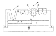
図1は、本発明の各実施形態によるトランジスタの断面図である。本発明によるトランジスタ、例えば、金属半導体電界効果トランジスタ(MESFET)について、以下に説明する。図1に示すように、まず、基板10を準備する。この基板10は、p導電型又はn導電型、あるいは半絶縁性のうちのいずれかの単結晶バルク炭化ケイ素(SiC)基板でよい。このp型又はn型の基板10は、極めて低濃度にドープすることができる。この基板を、6H、4H、15R、又は3C型の炭化ケイ素の群から選択された炭化ケイ素で形成することができる。本明細書では、本発明をSiC基板に関して説明するが、本発明をSiCに限定すべきではない。例えば、いくつかの実施形態では、基板10は、例えば、ガリウムヒ素(GaAs)及び/又は窒化ガリウム(GaN)を含むこともできる。
FIG. 1 is a cross-sectional view of a transistor according to each embodiment of the present invention. A transistor according to the present invention, for example a metal semiconductor field effect transistor (MESFET), is described below. As shown in FIG. 1, first, a
例えば、p導電型の炭化ケイ素の任意選択のバッファ層12を基板10上に設けることができる。このバッファ層12は、6H、4H、15R、又は3C型多結晶のp導電型炭化ケイ素で形成することができる。このバッファ層12のキャリア濃度は、例えば、約0.5×1015cm−3〜約3.0×1015cm−3でよい。適切なドーパントは、アルミニウム、ホウ素、及び/又はガリウムを含んでいる。バッファ素12の厚さは、約2.0μmでよい。このバッファ層12は、上述したようにp導電型炭化ケイ素として説明したが、本発明をこの構成に限定すべきではない。その代わりに、バッファ層12は、未ドープ(すなわち、意図的なドープ無しの)炭化ケイ素又は極めて低濃度にドープされたn導電型炭化ケイ素でもよい。極めて低濃度にドープされたn導電型炭化ケイ素がバッファ層12に使用される場合、このバッファ層12のキャリア濃度は、約5.0×1014cm−3未満であることが好ましい。
For example, an
さらに、図1に示すように、デバイスのドレインに向かって延びている端部を備えるデバイスのソースの下にp+領域14を設ける。本明細書で使用するとき、「p+」又は「n+」は、同一の層又は基板、あるいは他の層又は基板中に存在する、隣接する領域又は他の領域より高いキャリア濃度によって形成される領域を示している。本発明のある実施形態では、p+導電領域14は、ソースコンタクト26の下及び/又はn+ソース注入領域13の下から延びることができるが、n+ドレイン注入領域17の下までは延びていない。本発明の他の実施形態では、p+導電領域14は、ソースコンタクト26の下及び/又はn+ソース注入領域13の下から延びることができるが、ドレインコンタクト22の下までは延びていない。他の実施形態では、p+導電領域14は、さらに、ソースコンタクト26の下及び/又はn+ソース注入領域13の下からゲートの第1側壁31の下まで延びることができるが、ゲートの第1側壁31の下を越えない、あるいは、ソースコンタクト26の下及び/又はn+ソース注入領域13の下からゲートの第2側壁33の下まで延びることができるが、ゲートの第2側壁33の下を越えない、あるいは、ソースコンタクト26の下及び/又はn+ソース注入領域13の下からゲート24の第1側壁31と第2側壁33の間の下まで延びることができる。本発明のある実施形態では、p+導電領域14は、ソース側のゲート24の第1側壁31内の約0.1〜0.3μmの点まで延びることができる。
In addition, as shown in FIG. 1, a p + region 14 is provided under the source of the device with an end extending toward the drain of the device. As used herein, “p + ” or “n + ” is formed by a higher carrier concentration than adjacent regions or other regions present in the same layer or substrate, or other layers or substrates. Shows the area. In some embodiments of the present invention, the p +
p+領域14は、p導電型領域、例えば、p導電型炭化ケイ素である。このp+領域14の場合、約1.0×1018cm−3〜約1.0×1020cm−3のキャリア濃度が適切でないことがあるが、できるだけ高いキャリア濃度が好ましい。キャリア濃度は、p+領域14全体にわたって一定でないことがあるが、オーミックコンタクトのその上への形成に役立つように、p+領域14の表面でキャリア濃度ができるだけ高いことが好ましい。図3に示すように、本発明のいくつかの実施形態では、p+導電の領域14を基板10中に設けることができる。このp+導電の領域14は、例えば、バッファ層12又は基板10内に約0.4μm延びることができる。ソース領域の下のp+導電の領域14は、ソースからの電子の注入を禁止することができ、したがって、おそらく絶縁破壊電圧の向上をもたらすことができる。さらに、p+導電の領域14がドレイン領域の下まで延びないので、デバイス内に寄生特性(parasitic)が導入されるのを禁止することができ、したがって、デバイス性能に影響を及ぼさないようにすることができる。
The p + region 14 is a p conductivity type region, for example, p conductivity type silicon carbide. In the case of the p + region 14, a carrier concentration of about 1.0 × 10 18 cm −3 to about 1.0 × 10 20 cm −3 may not be appropriate, but a carrier concentration as high as possible is preferable. The carrier concentration, it is not constant over the entire p + region 14, to aid in the formation of the above it ohmic contact, as high as possible carrier concentration at the surface of the p + region 14 is preferred. As shown in FIG. 3, in some embodiments of the present invention, a p +
バッファ層12は、基板10と第2バッファ層16の間に設けることができる。この第2バッファ層16は、例えば、約1×1016cm−3〜5×1016cm−3、一般的には、約1.5×1016cm−3のキャリア濃度のp導電型炭化ケイ素でよい。また、このp導電型炭化ケイ素バッファ層16の厚さは、約0.5μm〜約1.0μmでよい。この第2バッファ層16は、上述したように、p導電型炭化ケイ素として説明したが、本発明をこの構成に限定すべきでない。例えば、その代わりに、バッファ層12に関して上述したように、この第2バッファ層16はn導電型のもの、例えば、極めて低濃度にドープされたn導電型SiC又は未ドープSiCでよい。図3に示すように、本発明のある実施形態では、この第2バッファ層16を基板10上に直接設けることができる。
The
図1に示すように、n導電型チャネル層18を第2バッファ層16上に設ける。このn導電型チャネル層18は、6H、4H、15R、又は3C型多結晶のn導電型炭化ケイ素で形成することができる。このn導電型炭化ケイ素チャネル層は、例えば、1つ又は複数の相異なるキャリア濃度のn導電型炭化ケイ素を含むことができる。例えば、図4に示すように、n導電型チャネル層18は、第1のn導電型チャネル層15及び第2のn導電型チャネル層19を備えることができる。その代わりにその開示が、あたかも本明細書にその全体が記載されているかのように本明細書に組み込まれている本発明の譲受人に譲渡されたSriramの特許文献6に詳細に記載されているように、このn導電型チャネル層18は、第1,第2及び第3のn導電型SiCを含むことができる。
As shown in FIG. 1, an n conductivity
さらに図1に示すように、デバイスのソース及びドレイン領域中に、n+領域13及びn+領域17をそれぞれ設ける。これらの領域13及び17は、一般的に、n導電型炭化ケイ素であり、n導電型チャネル層18のキャリア濃度より高いキャリア濃度を有する。これらのn+領域13及び17の場合、約1.0×1019cm−3のキャリア濃度が適切でないことがあるが、できるだけ高いキャリア濃度が好ましい。
Further, as shown in FIG. 1, an n + region 13 and an n + region 17 are provided in the source and drain regions of the device, respectively. These
これらの注入領域13及び17上にオーミックコンタクト26及び22をそれぞれ設け、ソースコンタクト26及びドレインコンタクト22を設けるためにそれらを隔てる。p+コンタクト25をもたらすためにp+導電領域14上にオーミックコンタクト25を設ける。好ましくは、オーミックコンタクト25,26、及び22は、ニッケル又は他の適切な金属で形成する。例えば、p+オーミックコンタクト25をソースコンタクト26に電気的に結合させることによって、p+導電領域14をソースと同一電位に維持する。酸化膜などの絶縁体層20をデバイスの露出表面上にさらに設けてもよい。
本発明のある実施形態によるトランジスタは、第1陥凹部43及びコンタクトビアホール42を備えている。第1陥凹部43を第1のn+領域13と第2のn+領域17の間、すなわち、ソースとドレインの間に設ける。第1陥凹部43は、n導電型チャネル層18の内部に延び、n導電型チャネル層18を露出させる。コンタクトビアホール42をソース領域13に隣接して設け、p+領域14の少なくとも一部分を露出させる。
The transistor according to an embodiment of the present invention includes a
図4に示すように、本発明の各実施形態によるトランジスタは、第1及び第2陥凹部を備えた二重陥凹構造とすることができる。具体的には、第1陥凹部53が、第2のn導電型チャネル層19を貫通して第1のn導電型チャネル層15まで延びる床面を備えている。第2陥凹部54を第1陥凹部の側壁61と62の間に設ける。第1陥凹部53の第1側壁61はソース26とゲート24の間にあり、第1陥凹部53の第2側壁62はドレイン22とゲート24の間にある。第2陥凹部54の床面60は、例えば、約600Åの距離、第1のn導電型チャネル層15の内部に延びている。この二重陥凹構造は、本発明の譲受人に譲渡されたSriramの特許文献6に記載されている。
As shown in FIG. 4, the transistor according to each embodiment of the present invention may have a double recessed structure including first and second recessed portions. Specifically, the
再度、図1を参照すると、ゲートコンタクト24をソース領域13とドレイン17の間の第1陥凹部43中に形成することができる。図4に示すように、上述したような本発明の二重陥凹部構造を備える各実施形態では、ゲート24を第2陥凹部中に設けることができる。さらに、図5に示すように、本発明のある実施形態では、ゲートコンタクト24をn導電型チャネル層18上に設け、例えば、第1陥凹部43又は第2陥凹部54中には設けないようにすることができる。
Referring again to FIG. 1, the
ゲートコンタクト24を、クロム、白金、白金シリサイド、ニッケル、及び/又は、TiWNで形成することができるが、ショトッキ(Schottky)効果を実現するために当業者に周知の金などの他の金属を使用することもできる。このショトッキゲートコンタクト24は、通常、3層構造を備えている。このような構造は、クロム(Cr)の高い接着力のため、有利なことがある。例えば、ゲートコンタクト24は、任意選択でn導電型チャネル層18に接触するクロム(Cr)の第1ゲート層を備えることができる。このゲートコンタクト24は、白金(Pt)及び金又は他の高導電率金属のオーバー層をさらに備えることもできる。その代わりに、このゲートコンタクト24は、n導電型チャネル層18上の第1陥凹部43中にニッケルの第1層を備えることもできる。このゲートコンタクト24は、金の層を含むニッケルの第1層上にオーバー層をさらに備えることもできる。
The
さらに、図1に示すように、金属のオーバー層28,30及び32を、それぞれ、ソースコンタクト26及びp+コンタクト25、ドレインコンタクト22、ならびにゲートコンタクト24上に設けることができる。これらの金属のオーバー層28,30及び32は、金,銀,アルミニウム,白金及び/又は銅でよい。他の適切な高導電率の金属をオーバー層に使用することもできる。さらに、金属のオーバー層28でp+領域14のp+コンタクト25をソースコンタクト26に結合することもできる。
Further, as shown in FIG. 1,
MESFETの寸法を選択する際、ゲートの幅は、電流の流れに垂直なゲートの寸法として定義する。図1の断面図に示すように、ゲート幅は、頁の上下を走る。ゲート長は、電流の流れに平行なゲート寸法である。図1の断面図に示すように、ゲート長は、n導電型チャネル層18と接触するゲート24の寸法である。例えば、本発明のある実施形態によるMESFETのゲート長は、約0.4μm〜約0.7μmでよい。他の重要な寸法は、ソース−ゲート間隔であり、これは図1の断面図に、ソースコンタクト26又はn+領域13からゲートコンタクト24までの間隔として示している。本発明のある実施形態によるソース−ゲート間隔は、約0.5μm〜約0.7μmでよい。さらにドレイン22からゲート24までの間隔は、約1.5μm〜約2μmでよい。本発明の各実施形態は、複数のMESFETの単位セルをさらに含むことができ、単位セルの第1ゲートから第2ゲートまでの間隔は、例えば、約20μm〜約50μmでよい。
When selecting the dimensions of the MESFET, the width of the gate is defined as the dimension of the gate perpendicular to the current flow. As shown in the cross-sectional view of FIG. 1, the gate width runs up and down the page. The gate length is the gate dimension parallel to the current flow. As shown in the cross-sectional view of FIG. 1, the gate length is the dimension of the
図2A乃至図2Hは、本発明の各実施形態によるFETの製造プロセスを示す図である。図2Aに示すように、まず、任意選択のバッファ層12を基板10上に成長又は堆積させる。この基板10は、半絶縁性SiC基板、p型基板又はn型基板でよい。この基板10は、極めて低濃度にドープすることができる。バッファ層12は、約3.0×1015cm−3以下、一般的には、約1.0×1015cm−3以下のキャリア濃度のp導電型炭化ケイ素でよい。その代わりに、このバッファ層12は、n型炭化ケイ素又は未ドープ炭化ケイ素でもよい。
2A to 2H are views showing a manufacturing process of the FET according to each embodiment of the present invention. As shown in FIG. 2A, an
基板10が、半絶縁性の場合、基板は、その開示が、あたかも本明細書にその全体が記載されているかのように本明細書に組み込まれている「Semi-insulating Silicon Carbide Without Vanadium Domination」という名称の本発明の譲受人に譲渡されたCarterらの特許文献7に記載のように製造することができる。このような半絶縁性基板は、炭化ケイ素基板の抵抗率が点欠陥に支配されるように、点欠陥レベルが十分高く、p型ドーパントとn型ドーパントのマッチングが十分なレベルの炭化ケイ素基板をもたらすことによって製造することができる。このような支配は、重金属、遷移元素、又は他のトラッピング準位の深い元素が約1×1016cm−3未満、好ましくは、約1.0×1014cm−3未満の濃度の原料粉末を用いて、高温で炭化ケイ素を製造することによって実現できる。例えば、約300℃〜約500℃未満のシード(種結晶;seed)を用いて、約2360℃以上2380℃以下の温度を使用することができる。すなわち、半絶縁性基板は、基板の抵抗率がこのような重金属又は遷移元素によって支配されないように、バナジウムなどの、重金属、遷移元素ドーパント、又は他のトラッピング準位の深い元素を実質的に含まないことが好ましい。半絶縁性基板は、重金属、遷移元素ドーパント、又は他のトラッピング準位の深い元素を実質的に含まないことが好ましいが、このような材料が本明細書に記載したMESFETの電気特性に実質的に影響を及ぼさない場合、このような元素は、本発明の開示からの利点を依然として保ちながら測定可能な量存在することができる。
If the
さらに、図2Aに示すように、p+領域14に注入するためにマスク45を形成する。このp+領域14は、一般的に、イオン、例えば、アルミニウム、ホウ素、及び/又はガリウムの注入と、その後の高温アニールによって形成する。適切なアニール温度は約1300〜1600℃、一般的には、約1500℃でよい。イオン注入は、図2Bに示すようなp+領域14を形成するためにマスク45によって覆われた領域上で実施することができる。すなわち、p導電型の高濃度にドープされた領域、例えば、p導電型炭化ケイ素をもたらすために、もしあればバッファ層12又は基板10の一部分に、イオンを注入する。注入すると直ぐにドーパントをアニールして注入領域を活性化させる。この高濃度にドープされたp導電型領域は、バッファ層12又は基板10の内部に約0.4μm延びることができる。
Further, as shown in FIG. 2A, a
次に、図2Bに示すように、第2バッファ層16及びn導電型チャネル層18をバッファ層12上に成長又は堆積させる。バッファ層12が含まれない場合、第2バッファ層16及びn導電型チャネル層18を基板10上に成長又は堆積させる。図2Bに示すように、第2バッファ層16をバッファ層12上に形成し、n導電型チャネル層18をこの第2バッファ層16上に形成する。
Next, as shown in FIG. 2B, the
次に、図2Cに示すように、n+領域13及び17に注入するためにマスク50を使用する。これらの領域13及び17は、一般的に、イオン、例えば、窒素(N)又はリン(P)の注入と、その後の高温アニールによって形成する。適切なアニール温度は約1100〜1600℃でよい。図2Dに示すように、n+領域13及び17を形成するためにマスク50によって覆われない領域上でイオン注入を実施することができる。すなわち、n導電型の高濃度にドープされた領域、例えば、n導電型チャネル層18より高いキャリア濃度のn導電型SiCをもたらすために、n導電型チャネル層18の一部分に、イオンを注入する。注入すると直ぐにドーパントをアニールして注入領域を活性化させる。
Next, as shown in FIG. 2C, a
次に、図2Dに示すように、基板10、バッファ層12、p+領域14、第2バッファ層16、及びn導電型チャネル層18をエッチングして素子分離メサを形成する。このメサは、基板10、バッファ層12、p+領域14、第2バッファ層16、及びn導電型チャネル層18によって形成される側壁55及び57を有し、それらはトランジスタの周縁部を構成する。このメサの側壁は、p+導電型領域14を越えて下に延びている。図2Dに示すように、メサを形成してデバイスの基板10の内部に延ばすことができる。このメサは、デバイスの空乏領域を越えて延び、デバイス中の電流の流れをメサに閉じ込めデバイスの静電容量を低下させることができる。好ましくは、上述したデバイスを反応性イオンエッチングによってメサを形成するが、当業者に周知の他の方法を用いてメサを形成することもできる。さらに、メサが利用されない場合、陽子照射、補償する原子でのカウンタードーピング、又は他の当業者に周知の方法などの、他の方法を使用してデバイスを素子分離することができる。
Next, as shown in FIG. 2D, the
ある実施形態では、第2バッファ層16及びn導電型チャネル層18のみをエッチングして図4に示すような素子分離メサを形成することができる。これらの実施形態において、第2バッファ層及びn導電型チャネル層18によって側壁55及び57が形成され、これらは、トランジスタの外縁部を構成する。
In some embodiments, only the
さらに、図2DにMESFETの第1陥凹部43の形成プロセスを示す。この第1陥凹部43は、マスク47を形成してこのマスク47を用いて第1陥凹部43を形成するためにn導電型チャネル層18をエッチングすることによって形成する。この第1陥凹部43は、乾式又は湿式エッチング法などのエッチング法によって形成することができる。例えば、この第1陥凹部43を、乾式エッチング、例えば、電子サイクロトロン共鳴(ECR;Electron Cyclotron Resonance)エッチング、又は誘導結合プラズマ(ICP;Inductively Coupled Plasma)エッチングによって形成することができる。次に、マスク47を除去する。
Further, FIG. 2D shows a process for forming the
上述したように、本発明の各実施形態では、単一陥凹部43の代わりに二重陥凹構造とすることができる。図4に示すように、二重陥凹構造の第1陥凹部53は、第1陥凹部53用のマスクを形成し、このマスクを使用して第1陥凹部53を形成するために第2のn導電型チャネル層19を貫通してエッチングすることによって形成する。絶縁層20は、この第1陥凹部53を形成した後で形成する。図2Gに示すようなオーミックコンタクトを形成した後で、第2陥凹部54用の第2マスクを形成し、このマスクを使用して第1陥凹部53をさらにエッチングすることによって、二重陥凹構造の第2陥凹部54を形成する。つまり、第1のn導電型チャネル層15を、例えば、約600Åエッチングして第2陥凹部54を形成することができる。さらに、二重陥凹構造の製造方法は、本発明の譲受人に譲渡されたSriramの特許文献6に記載されている。
As described above, in each embodiment of the present invention, a double recess structure can be used instead of the
図2Eに、上述したように第1陥凹部43を形成した後の、絶縁体層20、例えば、酸化膜層の形成プロセスを示す。この絶縁体層20は、既存の構造の露出表面、すなわち、素子分離メサ上、n+領域13上及び17上、n導電型チャネル層18上、ならびに第1陥凹部43中の上に成長又は堆積させる。酸化プロセスによって、例えば、エッチングプロセスにより損傷する恐れがあるSiCを除去することができ、エッチングによって表面上に発生する恐れがあるがある粗さを滑らかにすることもできる。
FIG. 2E shows a process for forming the
次に、図2Fに示すように、絶縁層20を貫通してn+領域13及び17までエッチングすることによりコンタクトウィンドウを形成する。また、高濃度にドープされたp+領域14の上の絶縁層20をエッチングすることにより第3のコンタクトウィンドウ41を形成する。次いで、ニッケルを蒸着させてソースコンタクト26及びドレインコンタクト22をそれぞれ堆積させる。このニッケルをアニールして図2Fに示すようなオーミックコンタクト26及び22を形成する。このような堆積及びアニールプロセスは、当業者にとって周知技術を用いて実施することができる。例えば、オーミックコンタクト26及び22を約950℃〜約1100℃の温度で約2分間アニールする。しかし、他の温度及び時間を使用することもできる。例えば、約30秒〜約10分の時間を許容することができる。
Next, as shown in FIG. 2F, a contact window is formed by etching through the insulating
次に、図2Gに示すようにMESFETのコンタクトビアホール42を形成する。このコンタクトビアホール42は、MESFETの絶縁層20中のウィンドウ41によって形成された部分内をエッチングすることによって形成される。n導電型チャネル層18及び第2バッファ層16を貫通してエッチングしてコンタクトビアホール42を形成するためにp+導電領域14を露出させる。エッチング法は、例えば、乾式又は湿式エッチング法でよい。さらに、図2Gに示すように、ニッケルを蒸着させてp+コンタクト25を堆積させる。次に、このニッケルをアニールしてオーミックコンタクト25を形成する。このような堆積及びアニールプロセスは、当業者にとって周知技術を用いて実施することができる。例えば、オーミックコンタクト25を約600℃〜約1050℃の温度でアニールすることができる。
Next, as shown in FIG. 2G, a contact via
次に、図2Hにゲートコンタクト24及びオーバー層28,30及び32を示す。例えば、絶縁体20中にウィンドウを開け、第1陥凹部43中にクロムの層を堆積させる。一般的に、クロム層は真空蒸着によって形成する。次いで、白金及び金の堆積によってゲート構造を完成させる。また、当業者には当然のことだが、これらのオーバー層28,30は、ゲート構造形成プロセスの前後のいずれかで形成することができる。実際、チタン/白金/金構造を使用する場合、オーバー層の白金及び金の部分は、ゲート構造の白金及び金の部分32と同じ処理ステップで形成することができる。したがって、オーバー層28及び30はゲートコンタクトの形成の前又は後で形成することができる。さらに、図示するように、ソースコンタクト26及びp+コンタクトは単一のオーバー層28を共有して、このオーバー層はソースが高濃度にドープされたp導電型領域14に電気的に結合させる。あるいは、上述したように、第1陥凹部43は二重陥凹構造でもよく、ゲートをこの二重陥凹構造内に設けることもできる。
Next, FIG. 2H shows the
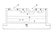
次に、図3を参照して、本発明の他の実施形態によるトランジスタの断面図について以下に説明する。なお、同一番号は、先に説明した図面における同一要素を示すもので、これらの要素の詳細な説明は省略する。図3に示すように、まず、基板10を準備する。この基板10は、例えば、SiC,GaAs又はGaNでよい。p+領域14をデバイスのソースの下に設け、その端部はデバイスのドレインに向かって延びている。本発明のいくつかの実施形態では、p+導電領域14は、ソースコンタクト26の下及び/又はn+ソース注入領域13から延び、n+ドレイン注入領域17の下まで延びている。また、本発明の他の実施形態では、p+導電領域14は、ソースコンタクト26の下及び/又はn+ソース注入領域13から延びているが、ドレインコンタクト22の下までは延びていない。図3に示すように、本発明の各実施形態では、p+導電領域14を基板10の内部に設ける。
Next, a cross-sectional view of a transistor according to another embodiment of the present invention will be described with reference to FIG. The same numbers indicate the same elements in the above-described drawings, and detailed descriptions of these elements are omitted. As shown in FIG. 3, first, the
第2バッファ層16を基板10及びp+導電領域14上に設ける。また、n導電型チャネル層18をこの第2バッファ層16上に設ける。また、n+領域13及び17を、それぞれデバイスのソース及びドレイン領域中に設ける。さらに、オーミックコンタクト26及び22をそれぞれソース注入領域13及び17上に設け、ソースコンタクト26及びドレインコンタクト22を形成するために各々は隔てられる。また、オーミックコンタクト25をp+導電領域14上に設けてp+コンタクト25を形成する。例えば、p+オーミックコンタクト25をソースコンタクト26に電気的に結合させることによって、このp+導電領域14をソースと同一電位に維持する。また、酸化膜などの絶縁体層20をデバイスの露出表面上にさらに設ける。
A
また、第1陥凹部43を第1のn+領域13と第2のn+領域17の間、すなわち、ソース領域とドレイン領域の間に設ける。この第1陥凹部43は、n導電型チャネル層18の内部に延び、このn導電型チャネル層18を露出させる。また、コンタクトビアホール42をソース領域13に隣接して設け、p+領域の少なくとも一部分を露出させる。また、ゲートコンタクト24を、ソース領域13とドレイン領域17の間の第1陥凹部43中に設ける。さらに、図3に示すように、金属オーバー層28,30及び32を、それぞれ、p+コンタクト26及び25、ドレインコンタクト22、ならびにゲートコンタクト24上に設ける。さらに、金属オーバー層28によってp+領域14のp+コンタクト25をソースコンタクト26に電気的に結合させる。
The
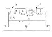
次に、図4を参照して、本発明の他の実施形態によるトランジスタの断面図にいて、以下に説明する。なお、同一番号は、先に説明した図面の同一要素を示すので、これらの要素の詳細な説明は省略する。図4に示すように、まず、基板10を準備する。この基板10は、例えば、SiC,GaAs又はGaNでよい。p+領域14をデバイスのソースの下に設け、その端部はデバイスのドレインに向かって延びている。本発明のいくつかの実施形態では、p+導電領域14は、ソースコンタクト26の下及び/又はn+ソース注入領域13から延びるが、n+ドレイン注入領域17の下までは延びていない。また、本発明の他の実施形態では、p+導電領域14は、ソースコンタクト26の下及び/又はn+ソース注入領域13から延びるが、ドレインコンタクト22の下までは延びていない。また、p+導電領域14を基板10の内部に設ける。また、バッファ層16を基板10及びp+導電領域14上に設ける。このバッファ層16は、例えば、キャリア濃度が約1.5×1016cm−3で、厚さが約0.5μmのp導電型炭化ケイ素でよい。
Next, referring to FIG. 4, a cross-sectional view of a transistor according to another embodiment of the present invention will be described below. In addition, since the same number shows the same element of drawing demonstrated previously, detailed description of these elements is abbreviate | omitted. As shown in FIG. 4, first, the
また、第1のn導電型チャネル層15をバッファ層16上に設ける。この第1のn導電型チャネル層15は、例えば、キャリア濃度が約3×1017cm−3で、厚さが約0.28μmでよい。また、第2のn導電型チャネル層19が、この第1のn導電型チャネル層15上にあってよく、それは、例えば、キャリア濃度が約1×1016cm−3、厚さが約900Åでよい。
A first n-conductivity
n+領域13及び17を、それぞれデバイスのソース及びドレイン領域中に設ける。オーミックコンタクト26及び22をそれぞれソース注入領域13及び17上に設け、ソースコンタクト26及びドレインコンタクト22を形成するために各々は隔てられる。また、オーミックコンタクト25をp+導電領域14上に設けてp+コンタクト25を形成する。例えば、p+オーミックコンタクト25をソースコンタクト26に電気的に結合させることによって、このp+導電領域14をソースと同一電位に維持する。また、酸化膜などの絶縁体層20をデバイスの露出表面上にさらに設ける。これらの第2バッファ層16、第1のn導電型チャネル層15及び第2のn導電型チャネル層19をエッチングして素子分離メサを形成することができる。図示するように、このメサはトランジスタの周縁部を構成する側壁55及び57を含んでいる。
N + regions 13 and 17 are provided in the source and drain regions of the device, respectively.
図4に示すように、図4のトランジスタ内に二重陥凹部が設けられる。この二重陥凹構造は、第1のn+領域13と第2のn+領域17の間、すなわち、ソース領域とドレイン領域の間に設ける。また、第1陥凹部53が、第2のn導電型チャネル層19を貫通して第1のn導電型チャネル層15まで延び、第1のn導電型チャネル層15を露出させる床面を備えている。ある実施形態では、この第1陥凹部53は、第1のn導電型チャネル層15の内部に延びることができる。また、第2陥凹部54を第1陥凹部の側壁61と62の間に設ける。また、第1陥凹部53の第1側壁61はソース26とゲート24の間にあり、第1陥凹部53の第2側壁62はドレイン22とゲート24の間にある。さらに、第2陥凹部54の床面60は、例えば、約600Åの距離、第1のn導電型チャネル層15の内部に延びている。
As shown in FIG. 4, a double recess is provided in the transistor of FIG. This double recessed structure is provided between the first n + region 13 and the second n + region 17, that is, between the source region and the drain region. The first recessed
また、ソース領域13に隣接してコンタクトビアホール42を設け、p+領域の少なくとも一部分を露出させる。ゲートコンタクト24をソース領域13とドレイン17の間の第2陥凹部54中に設ける。さらに、図4に示すように、金属のオーバー層28,30及び32を、それぞれ、ソースコンタクト26及びp+コンタクト25上、ドレインコンタクト22上、ならびにゲートコンタクト24上に設ける。さらに、金属のオーバー層28でp+領域14のp+コンタクト25をソースコンタクト26に結合する。
A contact via
次に、図5を参照して、本発明の他の実施形態によるMESFETの断面図について以下に説明する。なお、同一番号は、先に説明した図面の同一要素を示すので、これらの要素の詳細な説明は省略する。図5に示すように、ゲート24をn導電型チャネル層18上に設け、単一又は二重陥凹部中には設けない。
Next, a cross-sectional view of a MESFET according to another embodiment of the present invention will be described with reference to FIG. In addition, since the same number shows the same element of drawing demonstrated previously, detailed description of these elements is abbreviate | omitted. As shown in FIG. 5, the
次に、図6を参照して、本発明のある実施形態によるMESFETの平面(上面)図について以下に説明する。図6に示すように、基板10上に複数の単位セルを設ける。ゲート24はソース領域26とドレイン領域22の間に位置する。図6に示すように、ソースコンタクト26及びドレインコンタクト22は、相互に入り込んでいる。オーバー層28でソースコンタクト26をコンタクトビアホール43中に設けたp+コンタクト(図示せず)を介してp+領域(図示せず)に結合させる。
Next, referring to FIG. 6, a plan (top) view of a MESFET according to an embodiment of the present invention will be described below. As shown in FIG. 6, a plurality of unit cells are provided on the
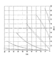
図7A及び図7Bは、それぞれ、従来のMESFETの低電圧及び高電圧でのドレインの電流−電圧特性をグラフに示す図である。また、図8A及び図8Bは、それぞれ、本発明の各実施形態によるMESFETの低電圧及び高電圧でのドレインの電流−電圧特性をグラフに示す図である。図7A乃至図8Bに示すデータは、同一ウェハ上に製作した従来のMESFETデバイス及び本発明の各実施形態によるMESFETデバイスから得たものである。これらのデバイスを同一ウェハ上に製作することで、ウェハ特性のばらつきに起因する不確定さの数を減少させることができる。 7A and 7B are graphs showing the current-voltage characteristics of the drain of the conventional MESFET at low voltage and high voltage, respectively. 8A and 8B are graphs showing drain current-voltage characteristics at low and high voltages of the MESFETs according to the embodiments of the present invention, respectively. The data shown in FIGS. 7A-8B were obtained from a conventional MESFET device fabricated on the same wafer and MESFET devices according to embodiments of the present invention. By manufacturing these devices on the same wafer, the number of uncertainties due to variations in wafer characteristics can be reduced.
図7A及び図8Aを参照すると、従来のMESFET及び本発明の各実施形態によるMESFETは、低ドレイン電圧では類似の特性を有している。しかし、図7B及び図8Bに示すように、高ドレイン電圧、すなわち、70ボルトを超えるドレイン電圧では、従来のMESFETは、過剰な漏れ電流及び低い相互コンダクタンスを示す(図7B)。これらのデバイス特性はこのようなデバイスのパワー出力及び高周波(RF)利得を劣化させることがある。対照的に、図8Bに示すように、p導電型層を含む本発明の各実施形態によるMESFETは、高ドレイン電圧で、漏れ電流の低下及び相互コンダクタンスの増大をもたらす。 Referring to FIGS. 7A and 8A, the conventional MESFET and the MESFET according to the embodiments of the present invention have similar characteristics at a low drain voltage. However, as shown in FIGS. 7B and 8B, at high drain voltages, ie, drain voltages exceeding 70 volts, conventional MESFETs exhibit excessive leakage current and low transconductance (FIG. 7B). These device characteristics can degrade the power output and radio frequency (RF) gain of such devices. In contrast, as shown in FIG. 8B, MESFETs according to embodiments of the present invention that include a p-conducting type layer result in reduced leakage current and increased transconductance at high drain voltages.
本発明を、特定の層、領域及び陥凹部を備える特定のMESFETに関して、上述したが、本発明の各実施形態は上述したMESFETに限定されないことは明らかである。また、ソース領域の下の本発明の各実施形態によるp導電型領域を、他のタイプのトランジスタ内に組み込むことができる。例えば、本発明の各実施形態によるp導電型領域を、その開示が、あたかも本明細書にその全体が記載されているかのように本明細書に組み込まれている「Silicon Carbide Metal Semiconductor Field Effect Transistors」という名称の本発明の譲受人に譲渡されたAllenらの特許文献8に記載されたMESFET内に組み込むことができる。 Although the present invention has been described above with respect to specific MESFETs with specific layers, regions and recesses, it is clear that embodiments of the present invention are not limited to the MESFETs described above. Also, the p-conductivity type region according to each embodiment of the present invention under the source region can be incorporated into other types of transistors. For example, a p-conductivity type region according to each embodiment of the present invention is disclosed in “Silicon Carbide Metal Semiconductor Field Effect Transistors”, the disclosure of which is incorporated herein as if fully set forth herein. Can be incorporated into the MESFET described in U.S. Pat.
上述したように、本発明の各実施形態によるトランジスタは、トランジスタのソース領域の下に、トランジスタのドレイン領域に向かって延びる端部を備えるp導電型領域を設けている。このタイプのp導電型領域を存在させることによって、例えば、他のデバイスの動作特性を損なうことなく絶縁破壊電圧が向上したデバイスを提供することができる。これによって、高い絶縁破壊電圧を得るためにデバイスの動作特性を犠牲にすることがある従来の電界効果トランジスタより優れた利点をもたらすことができる。 As described above, the transistor according to each embodiment of the present invention includes a p-conductivity type region having an end extending toward the drain region of the transistor below the source region of the transistor. The presence of this type of p-conductivity type region can provide a device having an improved breakdown voltage without impairing the operating characteristics of other devices, for example. This can provide advantages over conventional field effect transistors that can sacrifice device operating characteristics to achieve high breakdown voltages.
本発明をSiC MESFETに関して上述したが、本発明はSiC MESFETに限定されない。例えば、本発明の各実施形態によるMESFETは、例えば、ガリウムヒ素(GaAs)MESFET又は窒化ガリウム(GaN)MESFETでよい。具体的には、本発明をGaAs MESFETに関して説明した場合、p導電型領域はp導電型GaAs領域、n導電型チャネル層はn導電型GaAsチャネル層などでよいはずである。 Although the present invention has been described above with respect to SiC MESFETs, the present invention is not limited to SiC MESFETs. For example, the MESFET according to each embodiment of the present invention may be, for example, a gallium arsenide (GaAs) MESFET or a gallium nitride (GaN) MESFET. Specifically, when the present invention is described with reference to a GaAs MESFET, the p-conduction type region should be a p-conduction type GaAs region, the n-conduction type channel layer should be an n-conduction type GaAs channel layer, and the like.
図面及び明細書において、本発明の典型的な好ましい各実施形態を開示し、特定の用語を使用したが、これらは一般的に説明的な意味だけに使用したもので、これによって限定されるものではない。本発明の技術的範囲は、特許請求の範囲に記載されている。 In the drawings and specification, there have been disclosed exemplary preferred embodiments of the invention and specific terminology has been used, but these are generally used in a descriptive sense only and are limited thereby. is not. The technical scope of the present invention is described in the claims.
Claims (92)
前記ソースの下にあり、前記ドレインに向かって延びる端部を備え、前記n導電型チャネル層から隔てられて前記ソースに電気的に結合されているp導電型領域を備えたことを特徴とする金属半導体電界効果トランジスタ。 A source, a drain, and a gate, the gate being provided between the source and the drain and on the n-conducting channel layer;
A p-conductivity type region is provided below the source, having an end extending toward the drain and separated from the n-conductivity channel layer and electrically coupled to the source. Metal semiconductor field effect transistor.
前記ソースと前記ドレインの間にあって前記n導電型チャネル層を露出させ、前記ゲートがその中に設けられ、前記n導電型チャネル層内に延びる第1陥凹部と、
前記ソースに隣接し、前記p導電型領域を露出させるコンタクトビアホールと、
前記露出したp導電型領域上に設けられた第3のオーミックコンタクトと
をさらに備えたことを特徴とする請求項1に記載の金属半導体電界効果トランジスタ。 First and second ohmic contacts on the n-conducting channel layer constituting the source and drain, respectively;
A first recess between the source and the drain, exposing the n-conducting channel layer, the gate being provided therein, and extending into the n-conducting channel layer;
A contact via hole adjacent to the source and exposing the p conductivity type region;
The metal semiconductor field effect transistor according to claim 1, further comprising: a third ohmic contact provided on the exposed p conductivity type region.
前記ソースと前記ドレインの間にあって前記n導電型チャネル層を露出させ、第1及び第2側壁を備える第1陥凹部と、
前記第1陥凹部の前記第1側壁と前記第2側壁の間に配設され、前記ゲートがその中に設けられ前記n導電型チャネル層の内側に延びている第2陥凹部と、
前記ソースに隣接し、p導電型領域を露出させるコンタクトビアホールと、
前記露出p導電型領域上に設けられた第3のオーミックコンタクトと
をさらに備えたことを特徴とする請求項1に記載の金属半導体電界効果トランジスタ。 First and second ohmic contacts on the n conductivity type channel layer and constituting the source and the drain, respectively;
A first recess between the source and the drain, exposing the n-conducting channel layer and having first and second sidewalls;
A second recess disposed between the first sidewall and the second sidewall of the first recess, the gate being provided therein and extending inside the n-conducting channel layer;
A contact via hole adjacent to the source and exposing a p-conductivity type region;
The metal semiconductor field effect transistor according to claim 1, further comprising a third ohmic contact provided on the exposed p conductivity type region.
前記ソースの下にあり、前記ドレインに向かって延びている端部を備え、前記n導電型SiCチャネル層から隔てられ前記ソースに電気的に結合されている前記p導電型SiC領域と
を備えたことを特徴とする金属半導体電界効果トランジスタ。 A silicon carbide (SiC) comprising a source and a drain jump gate, wherein the gate is between the source and the drain and on a channel layer of n conductivity type SiC;
The p-conducting SiC region below the source and having an end extending toward the drain and separated from the n-conducting SiC channel layer and electrically coupled to the source; A metal semiconductor field effect transistor characterized by the above.
前記ソースの下にあり、前記ドレインに向かって延びる端部を備え、前記n導電型SiCチャネル層から隔てられ前記ソースに電気的に結合されているp導電型領域を形成するステップと
を有することを特徴とする金属半導体電界効果トランジスタの作製方法。 Forming a gate between the source and the drain and on the n-conducting channel layer, comprising: a source; a drain; and a gate;
Forming a p-conductivity type region below the source and having an end extending toward the drain and separated from the n-conductivity type SiC channel layer and electrically coupled to the source. A method for manufacturing a metal semiconductor field effect transistor.
前記p導電型領域を形成するステップは、前記ソースの下から前記ゲートの前記第1側壁まで延びていて前記ゲートの前記第1側壁を越えては延びていない前記p導電型領域を形成するステップを有することを特徴とする請求項48に記載の金属半導体電界効果トランジスタの作製方法。 The gate includes a first sidewall and a second sidewall, the first sidewall is on the source side of the gate, and the second sidewall is on the drain side of the gate,
The step of forming the p conductivity type region includes the step of forming the p conductivity type region that extends from under the source to the first side wall of the gate and does not extend beyond the first side wall of the gate. 49. The method for manufacturing a metal semiconductor field effect transistor according to claim 48, comprising:
前記p導電型領域を形成するステップは、前記ソースの下から前記第1側壁の前記ソース側上の前記ゲートの前記第1側壁の内側に約0.1〜約0.3μmまで延びている前記p導電型領域を形成するステップを有することを特徴とする請求項48に記載の金属半導体電界効果トランジスタの作製方法。 The gate includes a first sidewall and a second sidewall, the first sidewall is on the source side of the gate, and the second sidewall is on the drain side of the gate,
The step of forming the p-conductivity type region extends from below the source to the inside of the first sidewall of the gate on the source side of the first sidewall to about 0.1 to about 0.3 μm. 49. The method of manufacturing a metal semiconductor field effect transistor according to claim 48, further comprising a step of forming a p conductivity type region.
前記p導電型領域を形成するステップは、前記ソースの下から前記ゲートの前記第2側壁まで延びていて前記第2側壁を越えては延びていない前記p導電型領域を形成するステップを有することを特徴とする請求項48に記載の金属半導体電界効果トランジスタの作製方法。 The gate includes a first sidewall and a second sidewall, the first sidewall is on the source side of the gate, and the second sidewall is on the drain side of the gate,
The step of forming the p conductivity type region includes the step of forming the p conductivity type region extending from under the source to the second side wall of the gate and not extending beyond the second side wall. 49. A method of manufacturing a metal semiconductor field effect transistor according to claim 48.
前記p導電型領域を形成するステップは、前記ソースの下から前記ゲートの前記第1側壁と前記ゲートの前記第2側壁の間まで延びている前記p導電型領域を形成するステップを有することを特徴とする請求項48に記載の金属半導体電界効果トランジスタの作製方法。 The gate includes a first sidewall and a second sidewall, the first sidewall is on the source side of the gate, and the second sidewall is on the drain side of the gate,
The step of forming the p conductivity type region includes the step of forming the p conductivity type region extending from under the source to between the first sidewall of the gate and the second sidewall of the gate. 49. A method for manufacturing a metal semiconductor field effect transistor according to claim 48, wherein:
前記バッファ層中にp導電型ドーパントを注入するステップと、
前記p型ドーパントを活性化するために前記p型ドーパントをアニールするステップと
を有することを特徴とする請求項57に記載の金属半導体電界効果トランジスタの作製方法。 The step of forming the p conductivity type region includes:
Implanting a p-type dopant into the buffer layer;
58. The method of manufacturing a metal semiconductor field effect transistor according to claim 57, further comprising the step of annealing the p-type dopant to activate the p-type dopant.
SiC基板上に第1のキャリア濃度の第1のn導電型チャネル層を形成するステップと、
前記第1のn導電型チャネル層上に前記第1のn導電型チャネル層の前記第1のキャリア濃度より低いキャリア濃度の第2のn導電型チャネル層を形成するステップと
を有することを特徴とする請求項56に記載の金属半導体電界効果トランジスタの作製方法。 The step of forming the n conductivity type channel layer comprises the steps of:
Forming a first n-conductivity-type channel layer having a first carrier concentration on a SiC substrate;
Forming a second n conductivity type channel layer having a carrier concentration lower than the first carrier concentration of the first n conductivity type channel layer on the first n conductivity type channel layer. A method for manufacturing a metal semiconductor field effect transistor according to claim 56.
SiC基板上に第1のキャリア濃度の第1のn導電型チャネル層を形成するステップと、
前記第1のn導電型チャネル層上に第2のキャリア濃度の第2のn導電型チャネル層を形成するステップと、
前記第2のn導電型チャネル層上に第3のキャリア濃度の第3のn導電型チャネル層を形成するステップと
を有することを特徴とする請求項56に記載の金属半導体電界効果トランジスタの作製方法。 The step of forming the n conductivity type channel layer comprises the steps of:
Forming a first n-conductivity-type channel layer having a first carrier concentration on a SiC substrate;
Forming a second n-conductivity type channel layer having a second carrier concentration on the first n-conductivity type channel layer;
57. A metal semiconductor field effect transistor according to claim 56, further comprising: forming a third n conductivity type channel layer having a third carrier concentration on the second n conductivity type channel layer. Method.
前記n導電型チャネル層上及び前記第1陥凹部中に酸化膜層を形成するステップと、
前記n導電型チャネル層上に前記ソース及び前記ドレインをそれぞれ構成する第1及び第2のオーミックコンタクトを形成するステップと、
前記p導電型領域を露出させる前記ソースに隣接してコンタクトビアホールを形成するステップと、
前記露出したp導電型領域上に第3のオーミックコンタクトを形成するステップと
をさらに有することを特徴とする請求項48に記載の金属半導体電界効果トランジスタの作製方法。 Exposing the n-conducting channel layer between the source and the drain and forming a first recess extending inside the n-conducting channel layer in which the gate is formed;
Forming an oxide layer on the n-conducting channel layer and in the first recess;
Forming first and second ohmic contacts that constitute the source and the drain, respectively, on the n conductivity type channel layer;
Forming a contact via hole adjacent to the source exposing the p conductivity type region;
49. The method of manufacturing a metal semiconductor field effect transistor according to claim 48, further comprising: forming a third ohmic contact on the exposed p conductivity type region.
前記n導電型チャネル層上に前記第1陥凹部用のマスクを形成するステップと、
前記マスクに従って前記n導電型チャネル層内をエッチングするステップと
を有することを特徴とする請求項48に記載の金属半導体電界効果トランジスタの作製方法。 Forming the first depression includes:
Forming a mask for the first recess on the n-type channel layer;
49. The method of manufacturing a metal semiconductor field effect transistor according to claim 48, further comprising: etching the inside of the n conductivity type channel layer according to the mask.
前記p導電型層に隣接する酸化膜層中に前記コンタクトビアホール用のコンタクトウィンドウをエッチングするステップと、
前記p導電型層を露出させるために前記コンタクトウィンドウを貫通して前記n導電型チャネル層及び第2バッファ層をエッチングするステップと
を有することを特徴とする請求項68に記載の金属半導体電界効果トランジスタの作製方法。 The step of forming the contact via hole includes:
Etching a contact window for the contact via hole in an oxide film layer adjacent to the p conductivity type layer;
69. The metal semiconductor field effect of claim 68, further comprising: etching the n-conducting channel layer and the second buffer layer through the contact window to expose the p-conducting layer. A method for manufacturing a transistor.
前記ソースと前記ドレインと前記p導電型領域に隣接する前記酸化膜を貫通してコンタクトウィンドウをエッチングするステップと、
前記ソース及び前記ドレインに隣接する前記コンタクトウィンドウ中に前記第1及び第2のオーミックコンタクトを形成するステップと、
前記p導電型領域を露出させるために前記コンタクトウィンドウを貫通して前記n導電型チャネル層内及び第2バッファ層内をエッチングするステップと、
前記露出したp導電型層上に前記第3のオーミックコンタクトを形成するステップと
を有することを特徴とする請求項68に記載の金属半導体電界効果トランジスタの作製方法。 Forming the first, second and third ohmic contacts comprises:
Etching a contact window through the oxide adjacent to the source, the drain and the p-conductivity type region;
Forming the first and second ohmic contacts in the contact window adjacent to the source and the drain;
Etching the n-conducting channel layer and the second buffer layer through the contact window to expose the p-conducting region;
69. The method of manufacturing a metal semiconductor field effect transistor according to claim 68, further comprising: forming the third ohmic contact on the exposed p conductivity type layer.
前記ソースの第1オーミックコンタクト上及び前記p導電型領域の前記露出部分の第3のオーミックコンタクト上に、それぞれ第2のオーバー層を形成するステップとをさらに有し、前記第2のオーバー層が前記ソース上の前記第1のオーミックコンタクトを前記p導電型領域の露出部分の第3のオーミックコンタクトに電気的に結合させることを特徴とする請求項68に記載の金属半導体電界効果トランジスタの作製方法。 Forming a first overlayer on the second ohmic contact of the drain;
Forming a second overlayer on the first ohmic contact of the source and on the third ohmic contact of the exposed portion of the p-conductivity type region, respectively, the second overlayer comprising: 69. The method of manufacturing a metal semiconductor field effect transistor according to claim 68, wherein the first ohmic contact on the source is electrically coupled to a third ohmic contact of an exposed portion of the p conductivity type region. .
前記第1及び第2のオーミックコンタクトを形成するステップは、前記高濃度ドープ領域上に前記第1及び第2のオーミックコンタクトを形成するステップを有することを特徴とする請求項68に記載の金属半導体電界効果トランジスタの作製方法。 In order to provide a heavily doped region of n-conducting SiC having a higher carrier concentration than the n-conducting channel layer, an n-type dopant is provided in the SiC region of the n-conducting channel layer under the source and drain. And further comprising the step of injecting,
69. The metal semiconductor according to claim 68, wherein the step of forming the first and second ohmic contacts includes the step of forming the first and second ohmic contacts on the heavily doped region. A manufacturing method of a field effect transistor.
前記ソースと前記ドレインの間に、前記n導電型チャネル層を露出させて第1及び第2の側壁を備える第1陥凹部を形成するステップと、
前記第1陥凹部の前記第1側壁と前記第2側壁の間に、前記ゲートがその中に形成される前記n導電型チャネル層の内側に延びる第2陥凹部を形成するステップと、
前記p導電型領域を露出させる前記ソースに隣接してコンタクトビアホールを形成するステップと、
前記露出したp導電型領域上に第3のオーミックコンタクトを形成するステップと
をさらに有することを特徴とする請求項48に記載の金属半導体電界効果トランジスタの作製方法。 Forming first and second ohmic contacts that respectively constitute the source and the drain on the n-conducting channel layer;
Forming a first recess having first and second sidewalls by exposing the n-conducting channel layer between the source and the drain;
Forming a second recess between the first sidewall and the second sidewall of the first recess and extending inside the n-conducting channel layer in which the gate is formed;
Forming a contact via hole adjacent to the source exposing the p conductivity type region;
49. The method of manufacturing a metal semiconductor field effect transistor according to claim 48, further comprising: forming a third ohmic contact on the exposed p conductivity type region.
前記p導電型注入領域を注入し、p導電型SiC領域が、ソースの下にあり、ドレインに向かって延びている端部を備えるように、アニールで前記p導電型注入領域を活性化し、p導電型SiC領域を形成するステップであって、前記p導電型SiC領域がn導電型SiCチャネル層から隔てられ前記ソースに電気的に結合されており、前記n導電型SiCチャネル層は第1のn導電型SiCチャネル層及び第2のn導電型SiCチャネル層を含むステップと、
前記SiC基板及び前記p導電型SiC領域上にバッファ層を形成するステップと、
前記バッファ層上に前記第1のn導電型SiCチャネル層を形成するステップと、
前記第1のn導電型SiCチャネル層上に前記第2のn導電型SiCチャネル層を形成するステップと、
n導電型SiC注入用のマスクを形成するステップと、
前記n導電型SiCを注入し、前記第2のn導電型SiCチャネル層中でそれぞれソース及びドレイン領域を形成するためにアニールで前記n導電型SiCを活性化するステップと、
メサを形成するために前記第1及び第2のn導電型SiCチャネル層及び前記バッファ層をエッチングするステップと、
第1陥凹部用のマスクを形成し、前記ソース領域と前記ドレイン領域の間に前記第1陥凹部をエッチングするステップであって、前記第1陥凹部が前記第1のn導電型SiCチャネル層を露出させ第1及び第2の側壁を形成するステップと、
前記第1及び第2のn導電型SiCチャネル層上、前記第1陥凹部の前記ソース及び前記ドレイン領域上、ならびに前記第1陥凹部中に酸化膜層を形成するステップと、
前記酸化膜層中に前記ソースと前記ドレインとp導電型SiCコンタクト用のウィンドウを開けるステップと、
前記ソース及び前記ドレイン用に開けられた前記ウィンドウ中に第1及び第2のオーミックコンタクトを形成するステップと、
第2陥凹部用のマスクを形成し、前記第1陥凹部の前記第1側壁と前記第1側壁の間で前記第2のn導電型SiCチャネル層内に前記第2陥凹部をエッチングするステップと、
前記p導電型SiC領域を露出させるために、前記第1及び第2のn導電型チャネル層を貫通してエッチングし、前記コンタクトウィンドウを貫通して前記p導電型SiCコンタクト用の第2バッファ層をエッチングするステップと、
前記露出したp導電型SiC領域上に第3のオーミックコンタクトを形成するステップと、
前記第2陥凹部中にゲートを形成するステップと、
前記オーミックコンタクト及び前記ゲート上にオーバー層を形成するステップであって、前記ソース及び前記p導電型SiC領域の前記露出部分が、前記ソース及び前記p導電型SiC領域を電気的に結合させる単一のオーバー層を共有するステップと
を有することを特徴とする金属半導体電界効果トランジスタの作製方法。 Forming a p-conductivity type implantation mask on the SiC substrate;
Injecting the p-conductivity type implant region, annealing the p-conductivity type implant region so that the p-conductivity type SiC region has an end under the source and extending toward the drain, and p Forming a conductivity type SiC region, wherein the p conductivity type SiC region is separated from an n conductivity type SiC channel layer and is electrically coupled to the source, the n conductivity type SiC channel layer being a first conductivity type; including an n-conductivity type SiC channel layer and a second n-conductivity type SiC channel layer;
Forming a buffer layer on the SiC substrate and the p-conductivity type SiC region;
Forming the first n-conductivity-type SiC channel layer on the buffer layer;
Forming the second n-conductivity type SiC channel layer on the first n-conductivity type SiC channel layer;
forming a mask for n conductivity type SiC implantation;
Injecting the n-conductivity type SiC and activating the n-conductivity type SiC by annealing to form source and drain regions in the second n-conductivity type SiC channel layer, respectively;
Etching the first and second n-conductivity type SiC channel layers and the buffer layer to form mesas;
Forming a mask for a first recess, and etching the first recess between the source region and the drain region, wherein the first recess is the first n-conductivity-type SiC channel layer; Exposing first and second sidewalls; and
Forming an oxide layer on the first and second n-conductivity SiC channel layers, on the source and drain regions of the first recess, and in the first recess;
Opening a window for the source, drain, and p-conductivity type SiC contact in the oxide layer;
Forming first and second ohmic contacts in the window opened for the source and the drain;
Forming a mask for a second recess, and etching the second recess in the second n-conductivity-type SiC channel layer between the first sidewall and the first sidewall of the first recess. When,
Etching through the first and second n-conducting channel layers to expose the p-conducting SiC region, penetrating through the contact window and a second buffer layer for the p-conducting SiC contact Etching the step;
Forming a third ohmic contact on the exposed p-conductivity type SiC region;
Forming a gate in the second recess;
Forming an overlayer on the ohmic contact and the gate, wherein the exposed portion of the source and the p-conductivity-type SiC region electrically couples the source and the p-conductivity-type SiC region; And a step of sharing the overlayer of the metal semiconductor field effect transistor.
前記ソースの下にあり、前記ドレインに向かって延びている端部を備え、半導体材料の前記第1層から隔てられ前記ソースに電気的に結合されているp導電型領域を備えたことを特徴とするトランジスタ。 A transistor comprising a source, a drain and a gate, wherein the gate is between the source and the drain and on a first layer of semiconductor material;
A p-conductivity type region under the source, having an end extending toward the drain and spaced from the first layer of semiconductor material and electrically coupled to the source. A transistor.
87. The transistor of claim 86, further comprising an aluminum gallium nitride (AlGaN) based transistor.
Applications Claiming Priority (2)
| Application Number | Priority Date | Filing Date | Title |
|---|---|---|---|
| US10/304,272 US6956239B2 (en) | 2002-11-26 | 2002-11-26 | Transistors having buried p-type layers beneath the source region |
| PCT/US2003/031334 WO2004049454A1 (en) | 2002-11-26 | 2003-10-02 | Transistors having buried p-type layers beneath the source region and methods of fabricating the same |
Related Child Applications (1)
| Application Number | Title | Priority Date | Filing Date |
|---|---|---|---|
| JP2011284024A Division JP5758796B2 (en) | 2002-11-26 | 2011-12-26 | Transistor having p-type buried layer under source region and method for manufacturing the same |
Publications (1)
| Publication Number | Publication Date |
|---|---|
| JP2006507683A true JP2006507683A (en) | 2006-03-02 |
Family
ID=32325171
Family Applications (2)
| Application Number | Title | Priority Date | Filing Date |
|---|---|---|---|
| JP2004555310A Pending JP2006507683A (en) | 2002-11-26 | 2003-10-02 | A transistor including a p-type buried layer under a source region and a manufacturing method thereof. |
| JP2011284024A Expired - Lifetime JP5758796B2 (en) | 2002-11-26 | 2011-12-26 | Transistor having p-type buried layer under source region and method for manufacturing the same |
Family Applications After (1)
| Application Number | Title | Priority Date | Filing Date |
|---|---|---|---|
| JP2011284024A Expired - Lifetime JP5758796B2 (en) | 2002-11-26 | 2011-12-26 | Transistor having p-type buried layer under source region and method for manufacturing the same |
Country Status (11)
| Country | Link |
|---|---|
| US (2) | US6956239B2 (en) |
| EP (1) | EP1565946B1 (en) |
| JP (2) | JP2006507683A (en) |
| KR (1) | KR20050086758A (en) |
| CN (1) | CN100517761C (en) |
| AT (1) | ATE508477T1 (en) |
| AU (1) | AU2003277252A1 (en) |
| CA (1) | CA2502485A1 (en) |
| DE (1) | DE60337027D1 (en) |
| TW (1) | TWI329927B (en) |
| WO (1) | WO2004049454A1 (en) |
Cited By (19)
| Publication number | Priority date | Publication date | Assignee | Title |
|---|---|---|---|---|
| JP2007266475A (en) * | 2006-03-29 | 2007-10-11 | Furukawa Electric Co Ltd:The | Semiconductor device and power conversion apparatus |
| JP2007273640A (en) * | 2006-03-30 | 2007-10-18 | Sanken Electric Co Ltd | Semiconductor device |
| JP2007329205A (en) * | 2006-06-06 | 2007-12-20 | Matsushita Electric Ind Co Ltd | Transistor |
| JP2008507843A (en) * | 2004-07-23 | 2008-03-13 | クリー インコーポレイテッド | Method for fabricating a nitride-based transistor having a cap layer and a buried gate |
| JP2009182107A (en) * | 2008-01-30 | 2009-08-13 | Furukawa Electric Co Ltd:The | Semiconductor device |
| JP2010010412A (en) * | 2008-06-27 | 2010-01-14 | Furukawa Electric Co Ltd:The | Semiconductor element, and manufacturing method thereof |
| JP2010040814A (en) * | 2008-08-06 | 2010-02-18 | Sharp Corp | Semiconductor device |
| WO2011024367A1 (en) * | 2009-08-27 | 2011-03-03 | パナソニック株式会社 | Nitride semiconductor device |
| JP2011238805A (en) * | 2010-05-11 | 2011-11-24 | Nec Corp | Field effect transistor, method of manufacturing field effect transistor and electronic device |
| JP2012156320A (en) * | 2011-01-26 | 2012-08-16 | Toshiba Corp | Semiconductor element |
| WO2012114393A1 (en) * | 2011-02-23 | 2012-08-30 | パナソニック株式会社 | Nitride semiconductor device |
| JP2013175754A (en) * | 2009-04-21 | 2013-09-05 | Infineon Technologies Austria Ag | Horizontal hemt |
| JP2019519121A (en) * | 2016-06-24 | 2019-07-04 | クリー インコーポレイテッドCree Inc. | Gallium nitride high electron mobility transistor with P-type layer implanted deep into silicon carbide substrate |
| US10840334B2 (en) | 2016-06-24 | 2020-11-17 | Cree, Inc. | Gallium nitride high-electron mobility transistors with deep implanted p-type layers in silicon carbide substrates for power switching and radio frequency applications and process for making the same |
| US10892356B2 (en) | 2016-06-24 | 2021-01-12 | Cree, Inc. | Group III-nitride high-electron mobility transistors with buried p-type layers and process for making the same |
| JP2022519825A (en) * | 2019-01-28 | 2022-03-25 | クリー インコーポレイテッド | Group III nitride high electron mobility transistor with embedded p-type layer and its fabrication process |
| US11430882B2 (en) | 2016-06-24 | 2022-08-30 | Wolfspeed, Inc. | Gallium nitride high-electron mobility transistors with p-type layers and process for making the same |
| WO2023162521A1 (en) * | 2022-02-22 | 2023-08-31 | ローム株式会社 | Nitride semiconductor device and manufacturing method therefor |
| US11929428B2 (en) | 2021-05-17 | 2024-03-12 | Wolfspeed, Inc. | Circuits and group III-nitride high-electron mobility transistors with buried p-type layers improving overload recovery and process for implementing the same |
Families Citing this family (53)
| Publication number | Priority date | Publication date | Assignee | Title |
|---|---|---|---|---|
| US6686616B1 (en) * | 2000-05-10 | 2004-02-03 | Cree, Inc. | Silicon carbide metal-semiconductor field effect transistors |
| JP4009106B2 (en) * | 2001-12-27 | 2007-11-14 | 浜松ホトニクス株式会社 | Semiconductor light receiving element and manufacturing method thereof |
| JP4109159B2 (en) * | 2003-06-13 | 2008-07-02 | 浜松ホトニクス株式会社 | Semiconductor photo detector |
| JP4530171B2 (en) * | 2003-08-08 | 2010-08-25 | サンケン電気株式会社 | Semiconductor device |
| US20050139838A1 (en) * | 2003-12-26 | 2005-06-30 | Matsushita Electric Industrial Co., Ltd. | Semiconductor device and method for manufacturing semiconductor device |
| US7230274B2 (en) | 2004-03-01 | 2007-06-12 | Cree, Inc | Reduction of carrot defects in silicon carbide epitaxy |
| WO2005114746A1 (en) * | 2004-05-21 | 2005-12-01 | Nanyang Technological University | Novel structures of silicon carbide metal semiconductor field effect transistors for high voltage and high power applications |
| US20050275037A1 (en) * | 2004-06-12 | 2005-12-15 | Chung Shine C | Semiconductor devices with high voltage tolerance |
| US7345309B2 (en) * | 2004-08-31 | 2008-03-18 | Lockheed Martin Corporation | SiC metal semiconductor field-effect transistor |
| US20060091606A1 (en) * | 2004-10-28 | 2006-05-04 | Gary Paugh | Magnetic building game |
| US7265399B2 (en) | 2004-10-29 | 2007-09-04 | Cree, Inc. | Asymetric layout structures for transistors and methods of fabricating the same |
| US7348612B2 (en) * | 2004-10-29 | 2008-03-25 | Cree, Inc. | Metal-semiconductor field effect transistors (MESFETs) having drains coupled to the substrate and methods of fabricating the same |
| US7800097B2 (en) * | 2004-12-13 | 2010-09-21 | Panasonic Corporation | Semiconductor device including independent active layers and method for fabricating the same |
| US7326962B2 (en) * | 2004-12-15 | 2008-02-05 | Cree, Inc. | Transistors having buried N-type and P-type regions beneath the source region and methods of fabricating the same |
| JP4866007B2 (en) * | 2005-01-14 | 2012-02-01 | 富士通株式会社 | Compound semiconductor device |
| US8203185B2 (en) * | 2005-06-21 | 2012-06-19 | Cree, Inc. | Semiconductor devices having varying electrode widths to provide non-uniform gate pitches and related methods |
| US7598576B2 (en) * | 2005-06-29 | 2009-10-06 | Cree, Inc. | Environmentally robust passivation structures for high-voltage silicon carbide semiconductor devices |
| US7855401B2 (en) * | 2005-06-29 | 2010-12-21 | Cree, Inc. | Passivation of wide band-gap based semiconductor devices with hydrogen-free sputtered nitrides |
| US7525122B2 (en) * | 2005-06-29 | 2009-04-28 | Cree, Inc. | Passivation of wide band-gap based semiconductor devices with hydrogen-free sputtered nitrides |
| US7589378B2 (en) * | 2005-07-13 | 2009-09-15 | Texas Instruments Lehigh Valley Incorporated | Power LDMOS transistor |
| US7282765B2 (en) * | 2005-07-13 | 2007-10-16 | Ciclon Semiconductor Device Corp. | Power LDMOS transistor |
| US8692324B2 (en) * | 2005-07-13 | 2014-04-08 | Ciclon Semiconductor Device Corp. | Semiconductor devices having charge balanced structure |
| CA2622750C (en) * | 2005-09-16 | 2015-11-03 | The Regents Of The University Of California | N-polar aluminum gallium nitride/gallium nitride enhancement-mode field effect transistor |
| US7402844B2 (en) * | 2005-11-29 | 2008-07-22 | Cree, Inc. | Metal semiconductor field effect transistors (MESFETS) having channels of varying thicknesses and related methods |
| US7368971B2 (en) * | 2005-12-06 | 2008-05-06 | Cree, Inc. | High power, high frequency switch circuits using strings of power transistors |
| JP5008317B2 (en) * | 2006-02-27 | 2012-08-22 | 株式会社豊田中央研究所 | Unipolar diode |
| CA2584950A1 (en) * | 2006-04-26 | 2007-10-26 | Kansai Paint Co., Ltd. | Powder primer composition and method for forming coating film |
| US7646043B2 (en) * | 2006-09-28 | 2010-01-12 | Cree, Inc. | Transistors having buried p-type layers coupled to the gate |
| US7880172B2 (en) * | 2007-01-31 | 2011-02-01 | Cree, Inc. | Transistors having implanted channels and implanted P-type regions beneath the source region |
| JP5298470B2 (en) * | 2007-07-11 | 2013-09-25 | 三菱電機株式会社 | Semiconductor device and method for manufacturing semiconductor device |
| WO2009013886A1 (en) * | 2007-07-20 | 2009-01-29 | Panasonic Corporation | Silicon carbide semiconductor device and method for manufacturing the same |
| US7745846B2 (en) * | 2008-01-15 | 2010-06-29 | Ciclon Semiconductor Device Corp. | LDMOS integrated Schottky diode |
| US7781859B2 (en) * | 2008-03-24 | 2010-08-24 | Taiwan Semiconductor Manufacturing Company, Ltd. | Schottky diode structures having deep wells for improving breakdown voltages |
| US20090267145A1 (en) * | 2008-04-23 | 2009-10-29 | Ciclon Semiconductor Device Corp. | Mosfet device having dual interlevel dielectric thickness and method of making same |
| US9711633B2 (en) * | 2008-05-09 | 2017-07-18 | Cree, Inc. | Methods of forming group III-nitride semiconductor devices including implanting ions directly into source and drain regions and annealing to activate the implanted ions |
| JP4683141B2 (en) * | 2009-05-01 | 2011-05-11 | 住友電気工業株式会社 | Horizontal junction field effect transistor |
| KR20130126948A (en) | 2010-12-15 | 2013-11-21 | 이피션트 파워 컨버젼 코퍼레이션 | Semiconductor devices with back surface isolation |
| DE102011016900A1 (en) | 2011-04-13 | 2012-10-18 | Friedrich-Alexander-Universität Erlangen-Nürnberg | Semiconductor device |
| JP5877967B2 (en) * | 2011-07-19 | 2016-03-08 | 富士通株式会社 | Compound semiconductor device |
| US9812338B2 (en) | 2013-03-14 | 2017-11-07 | Cree, Inc. | Encapsulation of advanced devices using novel PECVD and ALD schemes |
| US9991399B2 (en) | 2012-10-04 | 2018-06-05 | Cree, Inc. | Passivation structure for semiconductor devices |
| US8994073B2 (en) | 2012-10-04 | 2015-03-31 | Cree, Inc. | Hydrogen mitigation schemes in the passivation of advanced devices |
| US9263571B2 (en) * | 2012-12-28 | 2016-02-16 | Hitachi, Ltd. | Silicon carbide semiconductor device and manufacturing method thereof |
| JP6143598B2 (en) | 2013-08-01 | 2017-06-07 | 株式会社東芝 | Semiconductor device |
| JP6534791B2 (en) * | 2013-12-16 | 2019-06-26 | ルネサスエレクトロニクス株式会社 | Semiconductor device |
| US9794401B2 (en) | 2015-01-06 | 2017-10-17 | Tracfone Wireless, Inc. | Methods, systems and applications for porting telephone numbers on wireless devices |
| CN105789282B (en) * | 2016-04-22 | 2019-01-25 | 西安电子科技大学 | There is one kind part high dopant channel 4H-SiC gold half field effect should manage |
| US10608079B2 (en) * | 2018-02-06 | 2020-03-31 | General Electric Company | High energy ion implantation for junction isolation in silicon carbide devices |
| TWI681530B (en) * | 2019-02-01 | 2020-01-01 | 力士科技股份有限公司 | Metal-oxide-semiconductor device |
| US20220367695A1 (en) * | 2021-05-17 | 2022-11-17 | Cree, Inc. | Circuits and group iii-nitride transistors with buried p-layers and controlled gate voltages and methods thereof |
| US20220376105A1 (en) * | 2021-05-20 | 2022-11-24 | Wolfspeed, Inc. | Field effect transistor with selective channel layer doping |
| US20230078017A1 (en) * | 2021-09-16 | 2023-03-16 | Wolfspeed, Inc. | Semiconductor device incorporating a substrate recess |
| US20230327026A1 (en) * | 2022-03-25 | 2023-10-12 | Wolfspeed, Inc. | Power semiconductor device with shallow conduction region |
Citations (15)
| Publication number | Priority date | Publication date | Assignee | Title |
|---|---|---|---|---|
| JPS61267369A (en) * | 1985-05-22 | 1986-11-26 | Hitachi Ltd | Field effect transistor |
| JPS62291975A (en) * | 1986-06-12 | 1987-12-18 | Matsushita Electric Ind Co Ltd | High-frequency semiconductor device |
| JPS6459961A (en) * | 1987-08-31 | 1989-03-07 | Toshiba Corp | Semiconductor device |
| JPH01304785A (en) * | 1988-06-01 | 1989-12-08 | Mitsubishi Electric Corp | Semiconductor integrated circuit |
| JPH04267531A (en) * | 1991-02-22 | 1992-09-24 | Hitachi Ltd | Compound semiconductor integrated circuit device |
| JPH0745695A (en) * | 1993-06-29 | 1995-02-14 | Yokogawa Electric Corp | Field-effect transistor |
| JPH08222578A (en) * | 1995-02-13 | 1996-08-30 | Nippon Telegr & Teleph Corp <Ntt> | Field effect transistor and its manufacture |
| JPH09260405A (en) * | 1996-03-27 | 1997-10-03 | Mitsubishi Electric Corp | Semiconductor device and manufacture thereof |
| JPH09283536A (en) * | 1996-04-15 | 1997-10-31 | Nec Corp | Field-effect transistor and manufacturing method thereof |
| JPH1027809A (en) * | 1996-07-10 | 1998-01-27 | Murata Mfg Co Ltd | Field-effect transistor |
| JPH11265896A (en) * | 1998-03-16 | 1999-09-28 | Toshiba Corp | Field effect transistor and its manufacturing method |
| JP2000349096A (en) * | 1999-06-01 | 2000-12-15 | Matsushita Electric Ind Co Ltd | Compound field effect transistor and its manufacture |
| JP2001308108A (en) * | 2000-04-19 | 2001-11-02 | Oki Electric Ind Co Ltd | Field effect transistor and its manufacturing method |
| WO2001086727A2 (en) * | 2000-05-10 | 2001-11-15 | Cree, Inc. | Silicon carbide metal-semiconductor field effect transistors and methods of fabricating silicon carbide metal-semiconductor field effect transistors |
| JP2002334890A (en) * | 2001-05-09 | 2002-11-22 | Matsushita Electric Ind Co Ltd | High-frequency power amplifier |
Family Cites Families (50)
| Publication number | Priority date | Publication date | Assignee | Title |
|---|---|---|---|---|
| JPS51424Y2 (en) | 1971-02-02 | 1976-01-08 | ||
| DE2324780C3 (en) * | 1973-05-16 | 1978-07-27 | Siemens Ag, 1000 Berlin Und 8000 Muenchen | Method for manufacturing a semiconductor component |
| JPS6051213B2 (en) | 1978-05-30 | 1985-11-13 | 株式会社フジクラ | Manufacturing equipment for flexible tape electric wire |
| JPS59134874A (en) | 1983-01-21 | 1984-08-02 | Hitachi Ltd | Semiconductor device |
| US4762806A (en) * | 1983-12-23 | 1988-08-09 | Sharp Kabushiki Kaisha | Process for producing a SiC semiconductor device |
| JPS60142568A (en) | 1983-12-29 | 1985-07-27 | Sharp Corp | Manufacture of sic field effect transistor |
| US4737469A (en) * | 1984-01-19 | 1988-04-12 | Honeywell Inc. | Controlled mode field effect transistors and method therefore |
| JPS60154674A (en) | 1984-01-25 | 1985-08-14 | Hitachi Ltd | Manufacture of electronic device |
| JPS60189250A (en) * | 1984-03-08 | 1985-09-26 | Fujitsu Ltd | Semiconductor device |
| EP0181091B1 (en) * | 1984-11-02 | 1990-06-13 | Kabushiki Kaisha Toshiba | Schottky gate field effect transistor and manufacturing method thereof |
| JP2615390B2 (en) * | 1985-10-07 | 1997-05-28 | 工業技術院長 | Method of manufacturing silicon carbide field effect transistor |
| EP0252179B1 (en) * | 1986-07-11 | 1992-05-27 | International Business Machines Corporation | Process for producing undercut mask profiles |
| JPS6347983A (en) | 1986-08-18 | 1988-02-29 | Sharp Corp | Silicon carbide field effect transistor |
| US5229625A (en) * | 1986-08-18 | 1993-07-20 | Sharp Kabushiki Kaisha | Schottky barrier gate type field effect transistor |
| JPH0797660B2 (en) | 1987-10-20 | 1995-10-18 | 三洋電機株式会社 | SiC blue light emitting diode |
| JPH0797659B2 (en) | 1987-10-20 | 1995-10-18 | 三洋電機株式会社 | SiC blue light emitting diode |
| US4947218A (en) * | 1987-11-03 | 1990-08-07 | North Carolina State University | P-N junction diodes in silicon carbide |
| JPH0798684B2 (en) | 1988-01-19 | 1995-10-25 | 日本碍子株式会社 | Method for manufacturing high density SiC sintered body |
| JPH01196873A (en) | 1988-02-02 | 1989-08-08 | Sharp Corp | Silicon carbide semiconductor device |
| JP2612040B2 (en) | 1988-06-28 | 1997-05-21 | 株式会社豊田中央研究所 | MOS-FET using β-SiC and manufacturing method thereof |
| US5014108A (en) * | 1990-05-15 | 1991-05-07 | Harris Corporation | MESFET for dielectrically isolated integrated circuits |
| JPH04225534A (en) * | 1990-12-27 | 1992-08-14 | Fujitsu Ltd | Semiconductor device and manufacture thereof |
| JPH0547798A (en) * | 1991-01-31 | 1993-02-26 | Texas Instr Inc <Ti> | Gaas fet with resistive a1gaas |
| US5289015A (en) * | 1991-04-25 | 1994-02-22 | At&T Bell Laboratories | Planar fet-seed integrated circuits |
| US5264713A (en) * | 1991-06-14 | 1993-11-23 | Cree Research, Inc. | Junction field-effect transistor formed in silicon carbide |
| US5270554A (en) * | 1991-06-14 | 1993-12-14 | Cree Research, Inc. | High power high frequency metal-semiconductor field-effect transistor formed in silicon carbide |
| US5925895A (en) * | 1993-10-18 | 1999-07-20 | Northrop Grumman Corporation | Silicon carbide power MESFET with surface effect supressive layer |
| US5510630A (en) * | 1993-10-18 | 1996-04-23 | Westinghouse Electric Corporation | Non-volatile random access memory cell constructed of silicon carbide |
| US5396085A (en) * | 1993-12-28 | 1995-03-07 | North Carolina State University | Silicon carbide switching device with rectifying-gate |
| US5399883A (en) * | 1994-05-04 | 1995-03-21 | North Carolina State University At Raleigh | High voltage silicon carbide MESFETs and methods of fabricating same |
| US5686737A (en) * | 1994-09-16 | 1997-11-11 | Cree Research, Inc. | Self-aligned field-effect transistor for high frequency applications |
| SE9404452D0 (en) * | 1994-12-22 | 1994-12-22 | Abb Research Ltd | Semiconductor device having an insulated gate |
| JP3158973B2 (en) | 1995-07-20 | 2001-04-23 | 富士電機株式会社 | Silicon carbide vertical FET |
| US5972801A (en) * | 1995-11-08 | 1999-10-26 | Cree Research, Inc. | Process for reducing defects in oxide layers on silicon carbide |
| JP2728126B2 (en) * | 1995-12-25 | 1998-03-18 | 日本電気株式会社 | Field effect transistor |
| US5719409A (en) * | 1996-06-06 | 1998-02-17 | Cree Research, Inc. | Silicon carbide metal-insulator semiconductor field effect transistor |
| DE19644821C1 (en) | 1996-10-29 | 1998-02-12 | Daimler Benz Ag | Controllable semiconductor structure for use instead of JFET, MESFET |
| US5742082A (en) * | 1996-11-22 | 1998-04-21 | Motorola, Inc. | Stable FET with shielding region in the substrate |
| US5891769A (en) * | 1997-04-07 | 1999-04-06 | Motorola, Inc. | Method for forming a semiconductor device having a heteroepitaxial layer |
| US6121633A (en) * | 1997-06-12 | 2000-09-19 | Cree Research, Inc. | Latch-up free power MOS-bipolar transistor |
| JPH11150124A (en) * | 1997-09-12 | 1999-06-02 | Toshiba Corp | Field effect transistor and its manufacture |
| JP3216804B2 (en) | 1998-01-06 | 2001-10-09 | 富士電機株式会社 | Manufacturing method of silicon carbide vertical FET and silicon carbide vertical FET |
| US6107649A (en) * | 1998-06-10 | 2000-08-22 | Rutgers, The State University | Field-controlled high-power semiconductor devices |
| US6316793B1 (en) * | 1998-06-12 | 2001-11-13 | Cree, Inc. | Nitride based transistors on semi-insulating silicon carbide substrates |
| JP3129298B2 (en) * | 1998-11-11 | 2001-01-29 | 日本電気株式会社 | Field effect transistor and method of manufacturing the same |
| US6218680B1 (en) * | 1999-05-18 | 2001-04-17 | Cree, Inc. | Semi-insulating silicon carbide without vanadium domination |
| DE60033656T2 (en) | 2000-03-03 | 2007-06-21 | Matsushita Electric Industrial Co., Ltd., Kadoma | SEMICONDUCTOR DEVICE |
| JP2002252233A (en) * | 2001-02-22 | 2002-09-06 | Matsushita Electric Ind Co Ltd | Semiconductor device and method of manufacturing the same |
| US6458640B1 (en) * | 2001-06-04 | 2002-10-01 | Anadigics, Inc. | GaAs MESFET having LDD and non-uniform P-well doping profiles |
| US6906350B2 (en) * | 2001-10-24 | 2005-06-14 | Cree, Inc. | Delta doped silicon carbide metal-semiconductor field effect transistors having a gate disposed in a double recess structure |
-
2002
- 2002-11-26 US US10/304,272 patent/US6956239B2/en not_active Expired - Lifetime
-
2003
- 2003-09-25 TW TW092126490A patent/TWI329927B/en not_active IP Right Cessation
- 2003-10-02 CA CA002502485A patent/CA2502485A1/en not_active Abandoned
- 2003-10-02 WO PCT/US2003/031334 patent/WO2004049454A1/en active Application Filing
- 2003-10-02 KR KR1020057009329A patent/KR20050086758A/en not_active Application Discontinuation
- 2003-10-02 EP EP03812016A patent/EP1565946B1/en not_active Expired - Lifetime
- 2003-10-02 AU AU2003277252A patent/AU2003277252A1/en not_active Abandoned
- 2003-10-02 CN CNB2003801044882A patent/CN100517761C/en not_active Expired - Lifetime
- 2003-10-02 AT AT03812016T patent/ATE508477T1/en not_active IP Right Cessation
- 2003-10-02 DE DE60337027T patent/DE60337027D1/en not_active Expired - Lifetime
- 2003-10-02 JP JP2004555310A patent/JP2006507683A/en active Pending
-
2005
- 2005-06-01 US US11/142,551 patent/US7297580B2/en not_active Expired - Lifetime
-
2011
- 2011-12-26 JP JP2011284024A patent/JP5758796B2/en not_active Expired - Lifetime
Patent Citations (16)
| Publication number | Priority date | Publication date | Assignee | Title |
|---|---|---|---|---|
| JPS61267369A (en) * | 1985-05-22 | 1986-11-26 | Hitachi Ltd | Field effect transistor |
| JPS62291975A (en) * | 1986-06-12 | 1987-12-18 | Matsushita Electric Ind Co Ltd | High-frequency semiconductor device |
| JPS6459961A (en) * | 1987-08-31 | 1989-03-07 | Toshiba Corp | Semiconductor device |
| JPH01304785A (en) * | 1988-06-01 | 1989-12-08 | Mitsubishi Electric Corp | Semiconductor integrated circuit |
| JPH04267531A (en) * | 1991-02-22 | 1992-09-24 | Hitachi Ltd | Compound semiconductor integrated circuit device |
| JPH0745695A (en) * | 1993-06-29 | 1995-02-14 | Yokogawa Electric Corp | Field-effect transistor |
| JPH08222578A (en) * | 1995-02-13 | 1996-08-30 | Nippon Telegr & Teleph Corp <Ntt> | Field effect transistor and its manufacture |
| JPH09260405A (en) * | 1996-03-27 | 1997-10-03 | Mitsubishi Electric Corp | Semiconductor device and manufacture thereof |
| JPH09283536A (en) * | 1996-04-15 | 1997-10-31 | Nec Corp | Field-effect transistor and manufacturing method thereof |
| JPH1027809A (en) * | 1996-07-10 | 1998-01-27 | Murata Mfg Co Ltd | Field-effect transistor |
| JPH11265896A (en) * | 1998-03-16 | 1999-09-28 | Toshiba Corp | Field effect transistor and its manufacturing method |
| JP2000349096A (en) * | 1999-06-01 | 2000-12-15 | Matsushita Electric Ind Co Ltd | Compound field effect transistor and its manufacture |
| JP2001308108A (en) * | 2000-04-19 | 2001-11-02 | Oki Electric Ind Co Ltd | Field effect transistor and its manufacturing method |
| WO2001086727A2 (en) * | 2000-05-10 | 2001-11-15 | Cree, Inc. | Silicon carbide metal-semiconductor field effect transistors and methods of fabricating silicon carbide metal-semiconductor field effect transistors |
| JP2003533051A (en) * | 2000-05-10 | 2003-11-05 | クリー インコーポレイテッド | Silicon carbide metal semiconductor field effect transistor and method of manufacturing silicon carbide metal semiconductor field effect transistor |
| JP2002334890A (en) * | 2001-05-09 | 2002-11-22 | Matsushita Electric Ind Co Ltd | High-frequency power amplifier |
Cited By (29)
| Publication number | Priority date | Publication date | Assignee | Title |
|---|---|---|---|---|
| JP2008507843A (en) * | 2004-07-23 | 2008-03-13 | クリー インコーポレイテッド | Method for fabricating a nitride-based transistor having a cap layer and a buried gate |
| US9666707B2 (en) | 2004-07-23 | 2017-05-30 | Cree, Inc. | Nitride-based transistors with a cap layer and a recessed gate |
| JP2007266475A (en) * | 2006-03-29 | 2007-10-11 | Furukawa Electric Co Ltd:The | Semiconductor device and power conversion apparatus |
| JP2007273640A (en) * | 2006-03-30 | 2007-10-18 | Sanken Electric Co Ltd | Semiconductor device |
| JP2007329205A (en) * | 2006-06-06 | 2007-12-20 | Matsushita Electric Ind Co Ltd | Transistor |
| JP2009182107A (en) * | 2008-01-30 | 2009-08-13 | Furukawa Electric Co Ltd:The | Semiconductor device |
| JP2010010412A (en) * | 2008-06-27 | 2010-01-14 | Furukawa Electric Co Ltd:The | Semiconductor element, and manufacturing method thereof |
| JP2010040814A (en) * | 2008-08-06 | 2010-02-18 | Sharp Corp | Semiconductor device |
| JP2013175754A (en) * | 2009-04-21 | 2013-09-05 | Infineon Technologies Austria Ag | Horizontal hemt |
| US8884335B2 (en) | 2009-04-21 | 2014-11-11 | Infineon Technologies Austria Ag | Semiconductor including lateral HEMT |
| WO2011024367A1 (en) * | 2009-08-27 | 2011-03-03 | パナソニック株式会社 | Nitride semiconductor device |
| JPWO2011024440A1 (en) * | 2009-08-27 | 2013-01-24 | パナソニック株式会社 | Nitride semiconductor device |
| CN102484124A (en) * | 2009-08-27 | 2012-05-30 | 松下电器产业株式会社 | Nitride semiconductor device |
| JP5526136B2 (en) * | 2009-08-27 | 2014-06-18 | パナソニック株式会社 | Nitride semiconductor device |
| WO2011024440A1 (en) * | 2009-08-27 | 2011-03-03 | パナソニック株式会社 | Nitride semiconductor device |
| JP2011238805A (en) * | 2010-05-11 | 2011-11-24 | Nec Corp | Field effect transistor, method of manufacturing field effect transistor and electronic device |
| JP2012156320A (en) * | 2011-01-26 | 2012-08-16 | Toshiba Corp | Semiconductor element |
| WO2012114393A1 (en) * | 2011-02-23 | 2012-08-30 | パナソニック株式会社 | Nitride semiconductor device |
| US8884332B2 (en) | 2011-02-23 | 2014-11-11 | Panasonic Corporation | Nitride semiconductor device |
| JP2019519121A (en) * | 2016-06-24 | 2019-07-04 | クリー インコーポレイテッドCree Inc. | Gallium nitride high electron mobility transistor with P-type layer implanted deep into silicon carbide substrate |
| US10840334B2 (en) | 2016-06-24 | 2020-11-17 | Cree, Inc. | Gallium nitride high-electron mobility transistors with deep implanted p-type layers in silicon carbide substrates for power switching and radio frequency applications and process for making the same |
| US10892356B2 (en) | 2016-06-24 | 2021-01-12 | Cree, Inc. | Group III-nitride high-electron mobility transistors with buried p-type layers and process for making the same |
| JP7009401B2 (en) | 2016-06-24 | 2022-01-25 | クリー インコーポレイテッド | Gallium Nitride High Electron Mobility Transistor with P-Type Layer Deeply Implanted in Silicon Carbide Substrate |
| US11430882B2 (en) | 2016-06-24 | 2022-08-30 | Wolfspeed, Inc. | Gallium nitride high-electron mobility transistors with p-type layers and process for making the same |
| US11862719B2 (en) | 2016-06-24 | 2024-01-02 | Wolfspeed, Inc. | Group III-nitride high-electron mobility transistors with buried p-type layers and process for making the same |
| JP2022519825A (en) * | 2019-01-28 | 2022-03-25 | クリー インコーポレイテッド | Group III nitride high electron mobility transistor with embedded p-type layer and its fabrication process |
| JP7248804B2 (en) | 2019-01-28 | 2023-03-29 | ウルフスピード インコーポレイテッド | Group III-nitride high electron mobility transistors with buried p-type layers and their fabrication process |
| US11929428B2 (en) | 2021-05-17 | 2024-03-12 | Wolfspeed, Inc. | Circuits and group III-nitride high-electron mobility transistors with buried p-type layers improving overload recovery and process for implementing the same |
| WO2023162521A1 (en) * | 2022-02-22 | 2023-08-31 | ローム株式会社 | Nitride semiconductor device and manufacturing method therefor |
Also Published As
| Publication number | Publication date |
|---|---|
| TW200419803A (en) | 2004-10-01 |
| US6956239B2 (en) | 2005-10-18 |
| CA2502485A1 (en) | 2004-06-10 |
| US20040099888A1 (en) | 2004-05-27 |
| CN1717811A (en) | 2006-01-04 |
| DE60337027D1 (en) | 2011-06-16 |
| ATE508477T1 (en) | 2011-05-15 |
| US20050224809A1 (en) | 2005-10-13 |
| CN100517761C (en) | 2009-07-22 |
| JP5758796B2 (en) | 2015-08-05 |
| TWI329927B (en) | 2010-09-01 |
| KR20050086758A (en) | 2005-08-30 |
| US7297580B2 (en) | 2007-11-20 |
| WO2004049454A1 (en) | 2004-06-10 |
| JP2012080123A (en) | 2012-04-19 |
| EP1565946B1 (en) | 2011-05-04 |
| AU2003277252A1 (en) | 2004-06-18 |
| EP1565946A1 (en) | 2005-08-24 |
Similar Documents
| Publication | Publication Date | Title |
|---|---|---|
| JP5758796B2 (en) | Transistor having p-type buried layer under source region and method for manufacturing the same | |
| US7348612B2 (en) | Metal-semiconductor field effect transistors (MESFETs) having drains coupled to the substrate and methods of fabricating the same | |
| US6906350B2 (en) | Delta doped silicon carbide metal-semiconductor field effect transistors having a gate disposed in a double recess structure | |
| US6686616B1 (en) | Silicon carbide metal-semiconductor field effect transistors | |
| JP4335283B2 (en) | Transistor having buried n-type and p-type regions under source region, and method for manufacturing the same | |
| US7402844B2 (en) | Metal semiconductor field effect transistors (MESFETS) having channels of varying thicknesses and related methods | |
| US7943972B2 (en) | Methods of fabricating transistors having buried P-type layers coupled to the gate |
Legal Events
| Date | Code | Title | Description |
|---|---|---|---|
| A621 | Written request for application examination |
Free format text: JAPANESE INTERMEDIATE CODE: A621 Effective date: 20060804 |
|
| A131 | Notification of reasons for refusal |
Free format text: JAPANESE INTERMEDIATE CODE: A131 Effective date: 20100827 |
|
| A601 | Written request for extension of time |
Free format text: JAPANESE INTERMEDIATE CODE: A601 Effective date: 20101126 |
|
| A602 | Written permission of extension of time |
Free format text: JAPANESE INTERMEDIATE CODE: A602 Effective date: 20101206 |
|
| A521 | Request for written amendment filed |
Free format text: JAPANESE INTERMEDIATE CODE: A523 Effective date: 20101227 |
|
| RD02 | Notification of acceptance of power of attorney |
Free format text: JAPANESE INTERMEDIATE CODE: A7422 Effective date: 20101207 |
|
| RD04 | Notification of resignation of power of attorney |
Free format text: JAPANESE INTERMEDIATE CODE: A7424 Effective date: 20110228 |
|
| A02 | Decision of refusal |
Free format text: JAPANESE INTERMEDIATE CODE: A02 Effective date: 20110823 |
|
| A521 | Request for written amendment filed |
Free format text: JAPANESE INTERMEDIATE CODE: A523 Effective date: 20111226 |
|
| A911 | Transfer to examiner for re-examination before appeal (zenchi) |
Free format text: JAPANESE INTERMEDIATE CODE: A911 Effective date: 20120106 |
|
| A912 | Re-examination (zenchi) completed and case transferred to appeal board |
Free format text: JAPANESE INTERMEDIATE CODE: A912 Effective date: 20120330 |
|
| A601 | Written request for extension of time |
Free format text: JAPANESE INTERMEDIATE CODE: A601 Effective date: 20120724 |
|
| A602 | Written permission of extension of time |
Free format text: JAPANESE INTERMEDIATE CODE: A602 Effective date: 20120727 |