JP4335283B2 - Transistor having buried n-type and p-type regions under source region, and method for manufacturing the same - Google Patents
Transistor having buried n-type and p-type regions under source region, and method for manufacturing the same Download PDFInfo
- Publication number
- JP4335283B2 JP4335283B2 JP2007546650A JP2007546650A JP4335283B2 JP 4335283 B2 JP4335283 B2 JP 4335283B2 JP 2007546650 A JP2007546650 A JP 2007546650A JP 2007546650 A JP2007546650 A JP 2007546650A JP 4335283 B2 JP4335283 B2 JP 4335283B2
- Authority
- JP
- Japan
- Prior art keywords
- region
- type conductive
- gate electrode
- sidewall
- type
- Prior art date
- Legal status (The legal status is an assumption and is not a legal conclusion. Google has not performed a legal analysis and makes no representation as to the accuracy of the status listed.)
- Active
Links
- 238000000034 method Methods 0.000 title claims abstract description 41
- 238000004519 manufacturing process Methods 0.000 title description 19
- 239000004065 semiconductor Substances 0.000 claims abstract description 24
- 230000005669 field effect Effects 0.000 claims abstract description 19
- HBMJWWWQQXIZIP-UHFFFAOYSA-N silicon carbide Chemical compound [Si+]#[C-] HBMJWWWQQXIZIP-UHFFFAOYSA-N 0.000 claims description 90
- 108091006146 Channels Proteins 0.000 claims description 84
- 239000000758 substrate Substances 0.000 claims description 84
- 229910010271 silicon carbide Inorganic materials 0.000 claims description 81
- JBRZTFJDHDCESZ-UHFFFAOYSA-N AsGa Chemical compound [As]#[Ga] JBRZTFJDHDCESZ-UHFFFAOYSA-N 0.000 claims description 25
- 229910001218 Gallium arsenide Inorganic materials 0.000 claims description 19
- 229910052751 metal Inorganic materials 0.000 claims description 18
- 239000002184 metal Substances 0.000 claims description 18
- JMASRVWKEDWRBT-UHFFFAOYSA-N Gallium nitride Chemical compound [Ga]#N JMASRVWKEDWRBT-UHFFFAOYSA-N 0.000 claims description 16
- 229910002601 GaN Inorganic materials 0.000 claims description 11
- 238000002513 implantation Methods 0.000 claims description 11
- 102000004129 N-Type Calcium Channels Human genes 0.000 claims description 8
- 108090000699 N-Type Calcium Channels Proteins 0.000 claims description 8
- 239000010410 layer Substances 0.000 description 142
- PXHVJJICTQNCMI-UHFFFAOYSA-N Nickel Chemical compound [Ni] PXHVJJICTQNCMI-UHFFFAOYSA-N 0.000 description 16
- 230000015556 catabolic process Effects 0.000 description 12
- 230000005684 electric field Effects 0.000 description 11
- 239000000463 material Substances 0.000 description 10
- BASFCYQUMIYNBI-UHFFFAOYSA-N platinum Chemical compound [Pt] BASFCYQUMIYNBI-UHFFFAOYSA-N 0.000 description 9
- 229910052759 nickel Inorganic materials 0.000 description 8
- 239000011651 chromium Substances 0.000 description 7
- 238000005530 etching Methods 0.000 description 7
- 239000012212 insulator Substances 0.000 description 7
- IJGRMHOSHXDMSA-UHFFFAOYSA-N Atomic nitrogen Chemical compound N#N IJGRMHOSHXDMSA-UHFFFAOYSA-N 0.000 description 6
- 238000005468 ion implantation Methods 0.000 description 6
- VYZAMTAEIAYCRO-UHFFFAOYSA-N Chromium Chemical compound [Cr] VYZAMTAEIAYCRO-UHFFFAOYSA-N 0.000 description 5
- 238000000137 annealing Methods 0.000 description 5
- 229910052804 chromium Inorganic materials 0.000 description 5
- 239000002019 doping agent Substances 0.000 description 5
- PCHJSUWPFVWCPO-UHFFFAOYSA-N gold Chemical compound [Au] PCHJSUWPFVWCPO-UHFFFAOYSA-N 0.000 description 5
- 229910052737 gold Inorganic materials 0.000 description 5
- 239000010931 gold Substances 0.000 description 5
- 230000008569 process Effects 0.000 description 5
- 230000015572 biosynthetic process Effects 0.000 description 4
- 239000011247 coating layer Substances 0.000 description 4
- 239000007943 implant Substances 0.000 description 4
- 238000002347 injection Methods 0.000 description 4
- 239000007924 injection Substances 0.000 description 4
- 238000002955 isolation Methods 0.000 description 4
- 229910052697 platinum Inorganic materials 0.000 description 4
- 229910052782 aluminium Inorganic materials 0.000 description 3
- XAGFODPZIPBFFR-UHFFFAOYSA-N aluminium Chemical compound [Al] XAGFODPZIPBFFR-UHFFFAOYSA-N 0.000 description 3
- 238000001312 dry etching Methods 0.000 description 3
- 230000000694 effects Effects 0.000 description 3
- 230000006872 improvement Effects 0.000 description 3
- 229910052757 nitrogen Inorganic materials 0.000 description 3
- ZOXJGFHDIHLPTG-UHFFFAOYSA-N Boron Chemical compound [B] ZOXJGFHDIHLPTG-UHFFFAOYSA-N 0.000 description 2
- GYHNNYVSQQEPJS-UHFFFAOYSA-N Gallium Chemical compound [Ga] GYHNNYVSQQEPJS-UHFFFAOYSA-N 0.000 description 2
- OAICVXFJPJFONN-UHFFFAOYSA-N Phosphorus Chemical compound [P] OAICVXFJPJFONN-UHFFFAOYSA-N 0.000 description 2
- XUIMIQQOPSSXEZ-UHFFFAOYSA-N Silicon Chemical compound [Si] XUIMIQQOPSSXEZ-UHFFFAOYSA-N 0.000 description 2
- 229910052796 boron Inorganic materials 0.000 description 2
- 239000000969 carrier Substances 0.000 description 2
- 230000008859 change Effects 0.000 description 2
- 238000007796 conventional method Methods 0.000 description 2
- 230000007423 decrease Effects 0.000 description 2
- 238000000151 deposition Methods 0.000 description 2
- 230000008021 deposition Effects 0.000 description 2
- 238000013461 design Methods 0.000 description 2
- 229910052733 gallium Inorganic materials 0.000 description 2
- 150000002500 ions Chemical class 0.000 description 2
- 238000001465 metallisation Methods 0.000 description 2
- 150000002739 metals Chemical class 0.000 description 2
- 230000003071 parasitic effect Effects 0.000 description 2
- 229910052698 phosphorus Inorganic materials 0.000 description 2
- 239000011574 phosphorus Substances 0.000 description 2
- 229910052710 silicon Inorganic materials 0.000 description 2
- 239000010703 silicon Substances 0.000 description 2
- 238000001039 wet etching Methods 0.000 description 2
- ZXEYZECDXFPJRJ-UHFFFAOYSA-N $l^{3}-silane;platinum Chemical compound [SiH3].[Pt] ZXEYZECDXFPJRJ-UHFFFAOYSA-N 0.000 description 1
- RYGMFSIKBFXOCR-UHFFFAOYSA-N Copper Chemical compound [Cu] RYGMFSIKBFXOCR-UHFFFAOYSA-N 0.000 description 1
- 208000034819 Mobility Limitation Diseases 0.000 description 1
- BQCADISMDOOEFD-UHFFFAOYSA-N Silver Chemical compound [Ag] BQCADISMDOOEFD-UHFFFAOYSA-N 0.000 description 1
- UQZIWOQVLUASCR-UHFFFAOYSA-N alumane;titanium Chemical compound [AlH3].[Ti] UQZIWOQVLUASCR-UHFFFAOYSA-N 0.000 description 1
- 150000001875 compounds Chemical class 0.000 description 1
- 229910052802 copper Inorganic materials 0.000 description 1
- 239000010949 copper Substances 0.000 description 1
- 230000008878 coupling Effects 0.000 description 1
- 238000010168 coupling process Methods 0.000 description 1
- 238000005859 coupling reaction Methods 0.000 description 1
- 239000013078 crystal Substances 0.000 description 1
- 230000007547 defect Effects 0.000 description 1
- 238000006731 degradation reaction Methods 0.000 description 1
- 238000009616 inductively coupled plasma Methods 0.000 description 1
- 238000011835 investigation Methods 0.000 description 1
- 238000005259 measurement Methods 0.000 description 1
- 229910044991 metal oxide Inorganic materials 0.000 description 1
- 150000004706 metal oxides Chemical class 0.000 description 1
- 238000004377 microelectronic Methods 0.000 description 1
- 229910021334 nickel silicide Inorganic materials 0.000 description 1
- RUFLMLWJRZAWLJ-UHFFFAOYSA-N nickel silicide Chemical compound [Ni]=[Si]=[Ni] RUFLMLWJRZAWLJ-UHFFFAOYSA-N 0.000 description 1
- 230000000704 physical effect Effects 0.000 description 1
- 238000001020 plasma etching Methods 0.000 description 1
- 229910021339 platinum silicide Inorganic materials 0.000 description 1
- 238000012545 processing Methods 0.000 description 1
- 230000009467 reduction Effects 0.000 description 1
- 230000004044 response Effects 0.000 description 1
- 229920006395 saturated elastomer Polymers 0.000 description 1
- 238000000926 separation method Methods 0.000 description 1
- 229910052709 silver Inorganic materials 0.000 description 1
- 239000004332 silver Substances 0.000 description 1
- 239000000243 solution Substances 0.000 description 1
- 229910052720 vanadium Inorganic materials 0.000 description 1
- LEONUFNNVUYDNQ-UHFFFAOYSA-N vanadium atom Chemical compound [V] LEONUFNNVUYDNQ-UHFFFAOYSA-N 0.000 description 1
- 238000007740 vapor deposition Methods 0.000 description 1
Images


Classifications
-
- H—ELECTRICITY
- H01—ELECTRIC ELEMENTS
- H01L—SEMICONDUCTOR DEVICES NOT COVERED BY CLASS H10
- H01L21/00—Processes or apparatus adapted for the manufacture or treatment of semiconductor or solid state devices or of parts thereof
- H01L21/02—Manufacture or treatment of semiconductor devices or of parts thereof
- H01L21/04—Manufacture or treatment of semiconductor devices or of parts thereof the devices having potential barriers, e.g. a PN junction, depletion layer or carrier concentration layer
- H01L21/18—Manufacture or treatment of semiconductor devices or of parts thereof the devices having potential barriers, e.g. a PN junction, depletion layer or carrier concentration layer the devices having semiconductor bodies comprising elements of Group IV of the Periodic Table or AIIIBV compounds with or without impurities, e.g. doping materials
-
- H—ELECTRICITY
- H01—ELECTRIC ELEMENTS
- H01L—SEMICONDUCTOR DEVICES NOT COVERED BY CLASS H10
- H01L29/00—Semiconductor devices specially adapted for rectifying, amplifying, oscillating or switching and having potential barriers; Capacitors or resistors having potential barriers, e.g. a PN-junction depletion layer or carrier concentration layer; Details of semiconductor bodies or of electrodes thereof ; Multistep manufacturing processes therefor
- H01L29/02—Semiconductor bodies ; Multistep manufacturing processes therefor
- H01L29/06—Semiconductor bodies ; Multistep manufacturing processes therefor characterised by their shape; characterised by the shapes, relative sizes, or dispositions of the semiconductor regions ; characterised by the concentration or distribution of impurities within semiconductor regions
- H01L29/0603—Semiconductor bodies ; Multistep manufacturing processes therefor characterised by their shape; characterised by the shapes, relative sizes, or dispositions of the semiconductor regions ; characterised by the concentration or distribution of impurities within semiconductor regions characterised by particular constructional design considerations, e.g. for preventing surface leakage, for controlling electric field concentration or for internal isolations regions
- H01L29/0607—Semiconductor bodies ; Multistep manufacturing processes therefor characterised by their shape; characterised by the shapes, relative sizes, or dispositions of the semiconductor regions ; characterised by the concentration or distribution of impurities within semiconductor regions characterised by particular constructional design considerations, e.g. for preventing surface leakage, for controlling electric field concentration or for internal isolations regions for preventing surface leakage or controlling electric field concentration
- H01L29/0611—Semiconductor bodies ; Multistep manufacturing processes therefor characterised by their shape; characterised by the shapes, relative sizes, or dispositions of the semiconductor regions ; characterised by the concentration or distribution of impurities within semiconductor regions characterised by particular constructional design considerations, e.g. for preventing surface leakage, for controlling electric field concentration or for internal isolations regions for preventing surface leakage or controlling electric field concentration for increasing or controlling the breakdown voltage of reverse biased devices
- H01L29/0615—Semiconductor bodies ; Multistep manufacturing processes therefor characterised by their shape; characterised by the shapes, relative sizes, or dispositions of the semiconductor regions ; characterised by the concentration or distribution of impurities within semiconductor regions characterised by particular constructional design considerations, e.g. for preventing surface leakage, for controlling electric field concentration or for internal isolations regions for preventing surface leakage or controlling electric field concentration for increasing or controlling the breakdown voltage of reverse biased devices by the doping profile or the shape or the arrangement of the PN junction, or with supplementary regions, e.g. junction termination extension [JTE]
- H01L29/0619—Semiconductor bodies ; Multistep manufacturing processes therefor characterised by their shape; characterised by the shapes, relative sizes, or dispositions of the semiconductor regions ; characterised by the concentration or distribution of impurities within semiconductor regions characterised by particular constructional design considerations, e.g. for preventing surface leakage, for controlling electric field concentration or for internal isolations regions for preventing surface leakage or controlling electric field concentration for increasing or controlling the breakdown voltage of reverse biased devices by the doping profile or the shape or the arrangement of the PN junction, or with supplementary regions, e.g. junction termination extension [JTE] with a supplementary region doped oppositely to or in rectifying contact with the semiconductor containing or contacting region, e.g. guard rings with PN or Schottky junction
-
- H—ELECTRICITY
- H01—ELECTRIC ELEMENTS
- H01L—SEMICONDUCTOR DEVICES NOT COVERED BY CLASS H10
- H01L29/00—Semiconductor devices specially adapted for rectifying, amplifying, oscillating or switching and having potential barriers; Capacitors or resistors having potential barriers, e.g. a PN-junction depletion layer or carrier concentration layer; Details of semiconductor bodies or of electrodes thereof ; Multistep manufacturing processes therefor
- H01L29/40—Electrodes ; Multistep manufacturing processes therefor
- H01L29/41—Electrodes ; Multistep manufacturing processes therefor characterised by their shape, relative sizes or dispositions
- H01L29/417—Electrodes ; Multistep manufacturing processes therefor characterised by their shape, relative sizes or dispositions carrying the current to be rectified, amplified or switched
- H01L29/41725—Source or drain electrodes for field effect devices
- H01L29/41766—Source or drain electrodes for field effect devices with at least part of the source or drain electrode having contact below the semiconductor surface, e.g. the source or drain electrode formed at least partially in a groove or with inclusions of conductor inside the semiconductor
-
- H—ELECTRICITY
- H01—ELECTRIC ELEMENTS
- H01L—SEMICONDUCTOR DEVICES NOT COVERED BY CLASS H10
- H01L29/00—Semiconductor devices specially adapted for rectifying, amplifying, oscillating or switching and having potential barriers; Capacitors or resistors having potential barriers, e.g. a PN-junction depletion layer or carrier concentration layer; Details of semiconductor bodies or of electrodes thereof ; Multistep manufacturing processes therefor
- H01L29/66—Types of semiconductor device ; Multistep manufacturing processes therefor
- H01L29/68—Types of semiconductor device ; Multistep manufacturing processes therefor controllable by only the electric current supplied, or only the electric potential applied, to an electrode which does not carry the current to be rectified, amplified or switched
- H01L29/76—Unipolar devices, e.g. field effect transistors
- H01L29/772—Field effect transistors
- H01L29/80—Field effect transistors with field effect produced by a PN or other rectifying junction gate, i.e. potential-jump barrier
- H01L29/812—Field effect transistors with field effect produced by a PN or other rectifying junction gate, i.e. potential-jump barrier with a Schottky gate
- H01L29/8128—Field effect transistors with field effect produced by a PN or other rectifying junction gate, i.e. potential-jump barrier with a Schottky gate with recessed gate
-
- H—ELECTRICITY
- H01—ELECTRIC ELEMENTS
- H01L—SEMICONDUCTOR DEVICES NOT COVERED BY CLASS H10
- H01L29/00—Semiconductor devices specially adapted for rectifying, amplifying, oscillating or switching and having potential barriers; Capacitors or resistors having potential barriers, e.g. a PN-junction depletion layer or carrier concentration layer; Details of semiconductor bodies or of electrodes thereof ; Multistep manufacturing processes therefor
- H01L29/02—Semiconductor bodies ; Multistep manufacturing processes therefor
- H01L29/12—Semiconductor bodies ; Multistep manufacturing processes therefor characterised by the materials of which they are formed
- H01L29/16—Semiconductor bodies ; Multistep manufacturing processes therefor characterised by the materials of which they are formed including, apart from doping materials or other impurities, only elements of Group IV of the Periodic Table
- H01L29/1608—Silicon carbide
-
- H—ELECTRICITY
- H01—ELECTRIC ELEMENTS
- H01L—SEMICONDUCTOR DEVICES NOT COVERED BY CLASS H10
- H01L29/00—Semiconductor devices specially adapted for rectifying, amplifying, oscillating or switching and having potential barriers; Capacitors or resistors having potential barriers, e.g. a PN-junction depletion layer or carrier concentration layer; Details of semiconductor bodies or of electrodes thereof ; Multistep manufacturing processes therefor
- H01L29/02—Semiconductor bodies ; Multistep manufacturing processes therefor
- H01L29/12—Semiconductor bodies ; Multistep manufacturing processes therefor characterised by the materials of which they are formed
- H01L29/20—Semiconductor bodies ; Multistep manufacturing processes therefor characterised by the materials of which they are formed including, apart from doping materials or other impurities, only AIIIBV compounds
- H01L29/2003—Nitride compounds
Landscapes
- Engineering & Computer Science (AREA)
- Microelectronics & Electronic Packaging (AREA)
- Power Engineering (AREA)
- Physics & Mathematics (AREA)
- Condensed Matter Physics & Semiconductors (AREA)
- General Physics & Mathematics (AREA)
- Computer Hardware Design (AREA)
- Ceramic Engineering (AREA)
- Manufacturing & Machinery (AREA)
- Junction Field-Effect Transistors (AREA)
- Solid State Image Pick-Up Elements (AREA)
- Metal-Oxide And Bipolar Metal-Oxide Semiconductor Integrated Circuits (AREA)
Abstract
Description
本発明は一般に、マイクロエレクトロニクスデバイスに関し、より詳細には、トランジスタ、例えば、金属半導体電界効果トランジスタ(MESFET)に関する。 The present invention relates generally to microelectronic devices, and more particularly to transistors, such as metal semiconductor field effect transistors (MESFETs).
近年、S帯域やX帯域の無線周波数などの高周波で動作しながらも、高パワー処理能力が求められる電気回路が、より普及してきている。高パワーの増大のため、高周波回路では、無線周波数およびそれよりも高い周波数で確実に動作可能でありながらも、より高いパワー負荷を処理することが可能なトランジスタの要望が増している。これまでは、バイポーラトランジスタ、およびパワー金属酸化膜半導体電界効果トランジスタ(MOSFET)が、高パワー用途に使用されてきたが、かかるデバイスのパワー処理能力は、より高い動作周波数に制限されることがある。接合電界効果トランジスタ(JFET)が、高周波用途に一般に使用されていたが、従来の周知のJFETのパワー処理能力もまた、制限されることがある。 In recent years, electric circuits that require high power processing capability while operating at high frequencies such as S-band and X-band radio frequencies have become more popular. Due to the increase in high power, there is an increasing demand for transistors capable of handling higher power loads while still reliably operating at radio frequencies and higher in high frequency circuits. To date, bipolar transistors and power metal oxide semiconductor field effect transistors (MOSFETs) have been used for high power applications, but the power handling capabilities of such devices may be limited to higher operating frequencies. . Although junction field effect transistors (JFETs) have been commonly used for high frequency applications, the power handling capabilities of conventional well known JFETs may also be limited.
金属半導体電界効果トランジスタ(MESFET)が、高周波用途のために開発されている。MESFETの構造は、多数キャリアだけが電流を搬送するため、高周波用途に好ましくなり得る。MESFETの設計は、ゲート容量の低減によって、ゲート入力のより迅速なスイッチング時間が可能となるため、MOSFETの設計よりも好ましくなり得る。したがって、電界効果トランジスタは全て、多数キャリアだけを利用して電流を搬送するものの、MESFETのショットキーゲート構造によって、MESFETは高周波用途により望ましくなり得る。 Metal semiconductor field effect transistors (MESFETs) have been developed for high frequency applications. The MESFET structure can be preferred for high frequency applications because only majority carriers carry current. The MESFET design may be preferred over the MOSFET design because the gate capacitance reduction allows for faster switching time of the gate input. Thus, although all field effect transistors use only majority carriers to carry current, the MESFET's Schottky gate structure may make MESFETs more desirable for high frequency applications.
構造のタイプに加えて、おそらくはより基本的には、トランジスタを形成する半導体材料の特性もまた、動作パラメータに影響を及ぼす。トランジスタの動作パラメータに影響を及ぼす特性のうち、電子移動度、飽和電子ドリフト速度、絶縁破壊電界、および熱伝導率が、トランジスタの高周波および高パワー特性に最も大きな影響を有し得る。 In addition to the type of structure, perhaps more fundamentally, the properties of the semiconductor material forming the transistor also affect the operating parameters. Of the characteristics that affect the operating parameters of the transistor, electron mobility, saturation electron drift velocity, breakdown electric field, and thermal conductivity can have the greatest influence on the high frequency and high power characteristics of the transistor.
電子移動度とは、電界の存在下で、電子がいかに迅速にその飽和速度まで加速されるかを示す測定値である。これまで、高い電子移動度を有する半導体材料が好まれていた。というのは、より多くの電流をより小さい電界で発生させることができ、そのため、電界を印加したときにより迅速な応答時間を得ることができたためである。飽和電子ドリフト速度とは、電子が半導体材料内で得ることができる最大速度である。より高い速度によって、ソースからドレインまでの時間がより短縮されることになるので、高周波用途にはより高い飽和電子ドリフト速度を有する材料が好ましくなり得る。 Electron mobility is a measurement that indicates how quickly electrons are accelerated to their saturation rate in the presence of an electric field. Heretofore, semiconductor materials having high electron mobility have been preferred. This is because more current can be generated with a smaller electric field, and thus a faster response time can be obtained when the electric field is applied. Saturated electron drift velocity is the maximum velocity at which electrons can be obtained in a semiconductor material. Materials with higher saturation electron drift velocities may be preferred for high frequency applications because higher speeds will reduce the time from source to drain.
絶縁破壊電界とは、ショットキー接合部が破壊され、デバイスのゲートを流れる電流が突然増大することになる電界強度である。所与の寸法の材料によって、一般により大きい電界を支持することができるので、高パワー、高周波トランジスタには絶縁破壊電界が高い材料が好ましくなり得る。より小さい電界よりも、より大きい電界によって電子をより迅速に加速することができるので、より大きい電界ではより高速な過渡現象(transient)が可能となる。 The breakdown electric field is the electric field strength at which the Schottky junction is destroyed and the current flowing through the gate of the device suddenly increases. Since a material of a given dimension can generally support a larger electric field, a material with a high breakdown field may be preferred for high power, high frequency transistors. Larger electric fields allow faster transients because electrons can be accelerated more quickly with larger electric fields than with smaller electric fields.
熱伝導率とは、半導体材料が熱を放散させる能力である。典型的な動作では、全てのトランジスタは熱を発生する。そして、高パワーおよび高周波トランジスタは通常、小信号トランジスタよりも多くの熱量を発生する。半導体材料の温度が増大するにつれて、接合部リーク電流が一般に増大し、温度の上昇に伴うキャリア移動度の減少のため、電界効果トランジスタを流れる電流は一般に低減する。したがって、半導体から熱を放散させると、その材料は低温のままとなり、より低いリーク電流でより多くの電流を搬送することが可能となる。 Thermal conductivity is the ability of a semiconductor material to dissipate heat. In typical operation, all transistors generate heat. And high power and high frequency transistors typically generate more heat than small signal transistors. As the temperature of the semiconductor material increases, the junction leakage current generally increases and the current through the field effect transistor generally decreases due to the decrease in carrier mobility with increasing temperature. Thus, when heat is dissipated from the semiconductor, the material remains at a low temperature and can carry more current with lower leakage current.
高周波MESFETは、それらの電子移動度が高いため、ガリウム砒素(GaAs)などのn型III−V族化合物で製造することができる。これらのデバイスによって、動作周波数の増大、およびパワー処理能力の適度な増大が実現されるものの、これらの材料は降伏電圧(breakdown voltage)が比較的低く、熱伝導率がより低いため、高パワー用途ではそれらの有用性が制限されてきた。 High-frequency MESFETs can be made of n-type III-V compounds such as gallium arsenide (GaAs) because of their high electron mobility. Although these devices provide an increased operating frequency and a modest increase in power handling capability, these materials have a relatively low breakdown voltage and lower thermal conductivity, resulting in higher power applications So their usefulness has been limited.
炭化ケイ素(SiC)が、ケイ素(Si)またはGaAsから製造されたデバイスよりも高温、高パワー、および高周波で動作することができる電子デバイスの製造を理論的に可能とする優れた物理特性および電子特性を有するとして長年知られている。約4×10⁶V/cmの高い絶縁電界、約2.0×107cm/秒の高い飽和電子ドリフト速度、および約4.9W/cm・Kの高い熱伝導率は、SiCが高周波、高パワー用途に適することを示している。 Excellent physical properties and electrons that allow silicon carbide (SiC) to theoretically produce electronic devices that can operate at higher temperatures, higher powers, and higher frequencies than devices made from silicon (Si) or GaAs Known for many years as having properties. A high insulating electric field of about 4 × 10 6 V / cm, a high saturation electron drift velocity of about 2.0 × 10 7 cm / sec, and a high thermal conductivity of about 4.9 W / cm · K, SiC is a high frequency, It is suitable for high power applications.
炭化ケイ素のチャネル層を有するMESFETが、シリコン基板上に製造されている(特許文献1および特許文献2参照)。MESFETの半導体層はエピタキシャルであるため、各エピタキシャル層をその上に成長させる層が、デバイスの特性に影響を及ぼす。したがって、Si基板上に成長させたSiCエピタキシャル層は、一般に、異なる基板上に成長させたSiCエピタキシャル層とは異なる電気特性および熱特性を有する。Si基板上にSiC層を成長させたデバイス(特許文献1および特許文献2参照)は、改善された熱特性を示すものの、Si基板の使用によって、一般に、かかるデバイスが熱を放散する能力が制限される。さらに、Si上のSiCの成長によって、一般に、エピタキシャル層に欠陥が生じ、そのため、デバイスの動作中に高いリーク電流が生じる。 MESFETs having a silicon carbide channel layer are manufactured on a silicon substrate (see Patent Document 1 and Patent Document 2). Since the semiconductor layer of MESFET is epitaxial, the layer on which each epitaxial layer is grown affects the device characteristics. Accordingly, SiC epitaxial layers grown on Si substrates generally have different electrical and thermal characteristics than SiC epitaxial layers grown on different substrates. Although devices with SiC layers grown on Si substrates (see Patent Literature 1 and Patent Literature 2) exhibit improved thermal properties, the use of Si substrates generally limits the ability of such devices to dissipate heat. Is done. Furthermore, the growth of SiC on Si generally results in defects in the epitaxial layer, which results in high leakage currents during device operation.
SiC基板を用いた他のMESFETも開発されている。例えば、SiC基板上に成長させたSiCエピタキシャル層を有するSiC MESFETが開示されている(特許文献3参照。本特許出願の開示の全体は、参照により本明細書に組み込まれる。)。これらのデバイスでは、SiC基板上に成長させたエピタキシャル層の結晶質の改善のため、従来のデバイスに優る、改善された熱特性が示された。しかし、高パワーおよび高周波を実現するには、SiCのより低い電子移動度の限界を克服する必要があろう。 Other MESFETs using SiC substrates have also been developed. For example, a SiC MESFET having a SiC epitaxial layer grown on a SiC substrate has been disclosed (see US Pat. No. 6,057,059, the entire disclosure of which is hereby incorporated by reference). These devices showed improved thermal properties over prior devices due to the improved crystallinity of the epitaxial layers grown on the SiC substrate. However, to achieve high power and high frequency, it would be necessary to overcome the lower electron mobility limitations of SiC.
同様に、SiCのn+領域上に形成されたソースおよびドレイン接点と、そこにチャネルが形成される、基板とn型層との間の任意選択の軽ドープエピタキシャル層とを有するSiC MESFETが開示されている(特許文献4参照)。また、高周波動作においてMESFETの性能を低減させ得る「表面効果(surface effect)」を克服すると説明されるSiC MESFETおよび構造が開示されている(特許文献5参照)。また、n+のソースおよびドレイン接点領域、ならびにp型バッファ層を使用したSiC MESFETについても開示されている(特許文献5参照)。SiC MESFETについては、さらに論じられている(特許文献6参照)。 Similarly, a SiC MESFET having source and drain contacts formed on an n + region of SiC and an optional lightly doped epitaxial layer between the substrate and the n-type layer in which a channel is formed is disclosed. (See Patent Document 4). Also disclosed are SiC MESFETs and structures that are described to overcome "surface effects" that can reduce the performance of MESFETs in high frequency operation (see Patent Document 5). An SiC MESFET using an n + source and drain contact region and a p-type buffer layer is also disclosed (see Patent Document 5). The SiC MESFET is further discussed (see Patent Document 6).
さらに、従来のSiC FET構造では、同様の導電型の軽ドープ領域によってゲートからオフセットされた非常に薄い高ドープチャネル(デルタドープチャネル)を用いることによって、FETの動作範囲全体にわたって、すなわち全開チャネルからピンチオフ電圧付近まで一定の特性をもたらすことができる。デルタドープチャネルについては、詳細に論じられている(例えば、非特許文献1および非特許文献2参照)。しかし、SiC MESFETにはさらなる改善を行うことができる。 In addition, conventional SiC FET structures use a very thin highly doped channel (delta doped channel) offset from the gate by a lightly doped region of similar conductivity type, thereby allowing the entire operating range of the FET, i.e., from a fully open channel. A certain characteristic can be provided up to the vicinity of the pinch-off voltage. The delta doped channel has been discussed in detail (for example, see Non-Patent Document 1 and Non-Patent Document 2). However, further improvements can be made to SiC MESFETs.
例えば、SiC MESFETを高効率、高パワー、高線形性無線周波数(RF)用途に使用する場合、SiC MESFETが高い降伏電圧、および比較的低いリーク電流を有することが重要となり得る。高い降伏電圧の実現を試みる中で、バナジウムドープ半絶縁SiCなど、高度に補償された(highly compensated)基板を有するデバイスが形成されている。これらのデバイスでは、一般に、適切な降伏電圧、ならびに低いリーク電流が実現されるが、基板中の望ましくないトラップ効果(trapping effect)のため、デバイス性能が犠牲になるおそれがある。さらに、FETのチャネル下に高ドープp型層を有するデバイスが形成され、良好な電子閉じ込めおよび低リーク電流を実現することに成功している。しかし、これらのデバイスは、一般に、デバイスのRF性能を劣化させ得る過剰な寄生(parasitic)を含む。したがって、デバイスの他の動作特性を犠牲にせずに、降伏電圧の改善を実現することができるように、既存のSiC FETデバイスにさらなる改善を行うことができる。 For example, if a SiC MESFET is used for high efficiency, high power, high linearity radio frequency (RF) applications, it may be important for the SiC MESFET to have a high breakdown voltage and a relatively low leakage current. In an attempt to achieve a high breakdown voltage, devices with highly compensated substrates, such as vanadium doped semi-insulating SiC, have been formed. These devices generally provide adequate breakdown voltage, as well as low leakage current, but device performance may be sacrificed due to undesirable trapping effects in the substrate. Furthermore, a device having a highly doped p-type layer under the channel of the FET has been formed, successfully achieving good electron confinement and low leakage current. However, these devices generally contain excessive parasitics that can degrade the RF performance of the device. Thus, further improvements can be made to existing SiC FET devices so that an improved breakdown voltage can be achieved without sacrificing other operating characteristics of the device.
本発明の目的とするところは、高周波で動作しながらも、より高いパワー負荷を処理することが可能な、動作特性を向上させたトランジスタおよびその製造法を提供することにある。 An object of the present invention is to provide a transistor with improved operating characteristics and a method of manufacturing the same, which can process a higher power load while operating at a high frequency.
本発明のいくつかの実施形態は、金属半導体電界効果トランジスタ(MESFET)のユニットセルを提供する。MESFETのユニットセルは、ソース領域、ドレイン領域、およびゲート電極を含むMESFETを含む。ゲート電極は、ソース領域とドレイン領域との間の、n型導電チャネル層上にある。p型導電領域が、ソース領域の下に設けられ、ドレイン領域の方に延びる端部を有する。このp型導電領域は、n型導電チャネル層から間隔を置いて配置され、ソース領域に電気的に結合される。n型導電領域が、ソース領域の下のp型導電領域上に設けられ、ドレイン領域の方に延びるが、p型導電領域の端部を越えては延びない。 Some embodiments of the present invention provide a unit cell of a metal semiconductor field effect transistor (MESFET). A unit cell of a MESFET includes a MESFET that includes a source region, a drain region, and a gate electrode . The gate electrode is on the n-type conductive channel layer between the source region and the drain region. A p-type conductive region is provided below the source region and has an end extending toward the drain region. The p-type conductive region is spaced from the n-type conductive channel layer and is electrically coupled to the source region. An n-type conductive region is provided on the p-type conductive region below the source region and extends toward the drain region, but does not extend beyond the end of the p-type conductive region.
本発明の他の実施形態では、p型導電領域は、第1のp型導電領域を含むことができる。ユニットセルは、第1のp型導電領域のキャリア濃度よりも低いキャリア濃度を有する第2のp型導電領域をさらに含むことができる。第2のp型導電領域は、第1のp型導電領域の端部からゲート電極の下まで延びることができ、したがって、第1および第2のp型導電領域は、n型導電領域の2つの表面に接して設けられることになる。ゲート電極は、第1の側壁および第2の側壁を有することができ、第1の側壁はソース領域に隣接し、第2の側壁はドレイン領域に隣接する。本発明の一実施形態では、第2のp型導電領域は、第1のp型導電領域の端部からゲート電極の第2の側壁まで、そのゲート電極の第2の側壁は越えずに延びるか、または、第1のp型導電領域の端部からゲート電極の第1の側壁と第2の側壁との間まで延びることができる。 In other embodiments of the present invention, the p-type conductive region may include a first p-type conductive region. The unit cell may further include a second p-type conductive region having a carrier concentration lower than that of the first p-type conductive region. The second p-type conductive region can extend from the end of the first p-type conductive region to the bottom of the gate electrode , and therefore the first and second p-type conductive regions are two of the n-type conductive region. It will be provided in contact with one surface. The gate electrode can have a first sidewall and a second sidewall, wherein the first sidewall is adjacent to the source region and the second sidewall is adjacent to the drain region. In one embodiment of the present invention, the second p-type conductive region from the end of the first p-type conductivity region to the second sidewall of the gate electrode, extending without exceeding the second sidewall of the gate electrode Alternatively, it can extend from the end of the first p-type conductive region to between the first side wall and the second side wall of the gate electrode .
本発明のさらに他の実施形態では、p型導電領域を露出させる接点バイアホール(contact via hole)を、ソース領域に隣接して設けることができる。n型導電領域は、p型導電領域のこの露出部分から延びることができるが、p型導電領域の端部を越えては延びない。MESFETを炭化ケイ素(SiC)基板などの基板上に設け、n型導電領域はこの基板中に延びることができる。n型導電領域は、基板中に約500Åから約1500Å延びることができるが、典型的には、基板中に約1000Å未満で延びる。 In yet another embodiment of the present invention, a contact via hole exposing the p-type conductive region can be provided adjacent to the source region. The n-type conductive region can extend from this exposed portion of the p-type conductive region, but does not extend beyond the end of the p-type conductive region. The MESFET can be provided on a substrate such as a silicon carbide (SiC) substrate, and the n-type conductive region can extend into the substrate. The n-type conductive region can extend from about 500 to about 1500 inches in the substrate, but typically extends less than about 1000 inches in the substrate.
本発明のいくつかの実施形態では、MESFETをバッファ層上に設け、n型導電領域はこのバッファ層中に延びることができる。n型導電領域は、バッファ層中に約500Åから約1500Åまで延びることができるが、典型的には、バッファ層中に約1000Å未満で延びる。本発明の一実施形態では、n型導電領域は、p型領域によって実質的に空乏化(deplete)させることができる。 In some embodiments of the invention, a MESFET may be provided on the buffer layer and the n-type conductive region may extend into the buffer layer. The n-type conductive region can extend from about 500 to about 1500 inches in the buffer layer, but typically extends less than about 1000 inches in the buffer layer. In one embodiment of the present invention, the n-type conductive region can be substantially depleted by the p-type region.
本発明のいくつかの実施形態では、ゲート電極は、第1の側壁および第2の側壁を有することができ、第1の側壁はソース領域に隣接し、第2の側壁はドレイン領域に隣接する。n型導電領域は、ソース領域の下からゲート電極の第1の側壁まで延びることができるが、ゲート電極の第1の側壁を越えては延びない。本発明の一実施形態では、n型導電領域は、ソース接点および/またはソース領域の下から延びることができるが、ドレイン接点の下までは延びない。 In some embodiments of the invention, the gate electrode can have a first sidewall and a second sidewall, wherein the first sidewall is adjacent to the source region and the second sidewall is adjacent to the drain region. . n-type conductive region may extend from below the source regions to the first sidewall of the gate electrode, it does not extend beyond the first side wall of the gate electrode. In one embodiment of the invention, the n-type conductive region can extend from below the source contact and / or source region, but does not extend below the drain contact.
本発明の他の実施形態では、基板は、炭化ケイ素(SiC)基板でよく、このSiC基板上にp型導電領域を配設することができる。n型導電チャネル層はn型導電SiCを含むことができ、p型導電領域はp型導電SiCを含むことができ、n型導電領域はn型導電SiCを含むことができる。 In other embodiments of the present invention, the substrate may be a silicon carbide (SiC) substrate, and a p-type conductive region may be disposed on the SiC substrate. The n-type conductive channel layer can include n-type conductive SiC, the p-type conductive region can include p-type conductive SiC, and the n-type conductive region can include n-type conductive SiC.
本発明のさらに他の実施形態では、基板を設け、この基板上にp型導電領域を配設することができる。基板は、ガリウム砒素(GaAs)または窒化ガリウム(GaN)を含むことができ、チャネル層は、GaAsまたはGaNとすることができ、p型導電領域は、p型導電GaAsまたはp型導電GaNとすることができ、n型導電領域は、n型導電GaAsまたはn型導電GaNとすることができる。 In yet another embodiment of the present invention, a substrate can be provided and a p-type conductive region can be disposed on the substrate. The substrate can include gallium arsenide (GaAs) or gallium nitride (GaN), the channel layer can be GaAs or GaN, and the p-type conductive region can be p-type conductive GaAs or p-type conductive GaN. The n-type conductive region can be n-type conductive GaAs or n-type conductive GaN.
本発明のいくつかの実施形態では、n型導電チャネル層中に、n型導電チャネル層のキャリア濃度よりも高いキャリア濃度を有するソース領域およびドレイン領域を画定するn型導電SiC注入領域を設けることができる。第1および第2のオーム接点(ohmic contact)を、ソース領域およびドレイン領域上にそれぞれ配設することができる。ゲート電極は、n型チャネル層中に配設することができる。ゲート電極は、n型チャネル層中の単一(single)または二重(double)凹部(recess)内に配設することができる。
In some embodiments of the present invention, an n-type conductive SiC implantation region is provided in the n-type conductive channel layer that defines a source region and a drain region having a carrier concentration higher than that of the n-type conductive channel layer. Can do. First and second ohmic contacts can be disposed on the source and drain regions, respectively. The gate electrode can be disposed in the n-type channel layer. The gate electrode can be disposed in a single or double recess in the n-type channel layer.
主に、MESFETに関して本発明を上記で説明してきたが、他のタイプのトランジスタ、ならびにトランジスタの製造方法、特に、MESFETの製造方法も提供される。 Although the present invention has been described above primarily with respect to MESFETs, other types of transistors, as well as methods for manufacturing transistors, and particularly methods for manufacturing MESFETs, are also provided.
本発明の実施形態を示す添付の図面を参照して、本発明を以下でより完全に説明する。しかし、本発明は、多数の異なる形態で実施することができ、本明細書に記載する実施形態のみに限定されるものと解釈すべきではない。そうではなく、以下の実施形態は、本開示を網羅的かつ完璧なものとし、本発明の範囲を当業者に完全に伝えるために示すものである。図面では、層および領域のサイズならびに相対サイズは、わかりやすいように誇張してあることがある。ある要素が、別の要素または層「の上に(on)」、「に連結される(connected to)」、または「結合される(coupled to)」と称される場合、その要素または層は、他方の要素または層のすぐ上にある、直接連結されている、または直接結合されているか、あるいは介在要素または層が存在し得ることが理解されよう。逆に、ある要素または層が別の要素または層「のすぐ上に(directly on)」、「に直接連結される(directly connected to)」、または「に直接結合される(directly coupled to)」と称される場合、介在要素または層は存在しない。本明細書では、用語「および/または(and/or)」は、列挙された関連する品目の1つまたは複数の任意の、およびあらゆる組合せを含む。同じ番号は、全体を通して同じ要素を指す。 The invention will be described more fully hereinafter with reference to the accompanying drawings, in which embodiments of the invention are shown. This invention may, however, be embodied in many different forms and should not be construed as limited to only the embodiments set forth herein; Rather, the following embodiments are presented so that this disclosure will be thorough and complete, and will fully convey the scope of the invention to those skilled in the art. In the drawings, the size and relative sizes of layers and regions may be exaggerated for clarity. When an element is referred to as “on”, “connected to”, or “coupled to” another element or layer, the element or layer is It will be appreciated that there may be intervening elements or layers, directly connected or directly coupled, directly above the other element or layer. Conversely, one element or layer is “directly on”, “directly connected to” or “directly coupled to” another element or layer. There are no intervening elements or layers. As used herein, the term “and / or” includes any and all combinations of one or more of the associated listed items. The same numbers refer to the same elements throughout.
本明細書では、用語「第1の」、及び「第2の」を用いて様々な領域、層、および/または区画を説明しているが、これらの領域、層、および/または区画は、これらの用語によって限定されるべきものではないことが理解されよう。これらの用語は、ある領域、層、または区画を別の領域、層、または区画から区別するために使用するにすぎない。したがって、本発明の教示から逸脱することなく、以下で論じる第1の領域、層、または区画を、第2の領域、層、または区画と呼ぶことができ、同様に、第2の領域、層、または区画を、第1の領域、層、または区画と呼ぶこともできる。 In this specification, the terms “first” and “second” are used to describe various regions, layers, and / or compartments. It will be understood that these terms should not be limited. These terms are only used to distinguish one region, layer or section from another region, layer or section. Accordingly, a first region, layer, or section discussed below can be referred to as a second region, layer, or section without departing from the teachings of the present invention, as well as a second region, layer, or layer. Or the compartment may be referred to as a first region, layer, or compartment.
さらに、本明細書では、「下部の(lower)」または「底部(bottom)」、および「上部の(upper)」または「頂部(top)」などの相対語を用いて、図に示すある要素と別の要素との位置関係を説明することがある。相対語は、図に描かれた向きに加えて、デバイスの異なる向きをも包含するものであることが理解されよう。例えば、図のデバイスを上下逆にした場合、他の要素の「下部(lower)」側にあると説明された要素は、他の要素の「上部(upper)」側に向くことになる。したがって、例示的な用語「下部の」は、図の特定の向きに応じて、「下部の」および「上部の」の両方の向きを包含し得る。同様に、図の1つのデバイスを上下逆にした場合、他の要素の「下の(below)」または「下に(beneath)」と説明された要素は、他の要素の「上に(above)」向くことになる。したがって、例示的な用語「下の」または「下に」は、上および下の両方の向きを包含し得る。 Further, herein, certain elements shown in the figures using relative terms such as “lower” or “bottom” and “upper” or “top”. May explain the positional relationship between and other elements. It will be understood that relative terms encompass different orientations of the device in addition to the orientation depicted in the figures. For example, if the illustrated device is turned upside down, an element that is described as being on the “lower” side of another element will face the “upper” side of the other element. Thus, the exemplary term “bottom” may encompass both “bottom” and “top” orientations, depending on the particular orientation of the figure. Similarly, when one device in the figure is turned upside down, an element described as “below” or “beneath” of another element is “above” the other element. ) ” Thus, the exemplary terms “down” or “down” may encompass both up and down orientations.
本発明の理想化された実施形態の概略図である断面図を参照しながら、本発明の実施形態を本明細書にて説明する。したがって、例えば、製造技術および/または製造公差の結果による、例示の図の形状からの変形形態が予想されるものである。したがって、本発明の実施形態は、本明細書に記載の特定の領域形状のみに限られるものと解釈すべきではなく、例えば製造から生じる形状の偏差も含むものである。例えば、長方形ウィル(will)として例示する注入領域は、典型的には、丸まった、または湾曲した形状を有し、かつ/または、その縁部では、注入領域から非注入領域への二元変化(binary change)ではなく、注入濃度の傾斜(gradient)を有する。同様に、注入によって形成される埋込み領域は、その埋込み領域と、注入がそこから行われる表面との間の領域に幾分かの注入をもたらすことになり得る。したがって、図に示す領域は概略的な性質のものであり、それらの形状は、デバイスの正確な領域形状を示すものではなく、また、本発明の範囲を限定するものでもない。 Embodiments of the present invention are described herein with reference to cross-section illustrations that are schematic illustrations of idealized embodiments of the present invention. Thus, for example, variations from the illustrated figure shape due to manufacturing techniques and / or manufacturing tolerance results are to be expected. Thus, embodiments of the present invention should not be construed as limited to the particular region shapes set forth herein but are to include deviations in shapes that result, for example, from manufacturing. For example, an injection region, exemplified as a rectangular will, typically has a rounded or curved shape and / or a binary change from an injection region to a non-injection region at its edges. Instead of (binary change), it has a gradient of the implantation concentration. Similarly, a buried region formed by implantation may result in some implantation in the region between the buried region and the surface from which the implantation takes place. Accordingly, the regions shown in the figures are of a general nature and their shape does not represent the exact region shape of the device and does not limit the scope of the invention.
本明細書で使用する用語は、特定の実施形態を説明するためのものにすぎず、本発明を限定するものではない。本明細書では、単数形「1つの(a、an)」および「その(the)」は、文脈において別段の明白な指示がない限り、その複数形も同様に含むものである。さらに、用語「備える(comprises)」および/または「備えている(comprising)」は、本明細書では、記載された特徴、実体物(integer)、ステップ、動作、要素、および/または構成要素の存在を明示するが、1つまたは複数の他の特徴、実体物、ステップ、動作、要素、構成要素、および/またはそれらの群の存在または追加を排除するものではないことが理解されよう。 The terminology used herein is for the purpose of describing particular embodiments only and is not intended to be limiting of the invention. As used herein, the singular forms “a” and “the” include the plural forms as well, unless the context clearly indicates otherwise. Further, the terms “comprises” and / or “comprising” are used herein to describe the described features, entities, steps, operations, elements, and / or components. It will be understood that the presence is not intended to exclude the presence or addition of one or more other features, entities, steps, actions, elements, components, and / or groups thereof.
本明細書で使用する用語(技術的および科学的用語を含む)は全て、別段の定義がない限り、本発明が属する分野の当業者によって一般に理解されている意味と同じ意味を有する。さらに、一般に使用されている辞書に定義されているものなどの用語は、関連技術の例における意味と一致する意味を有するものとして解釈すべきであり、本明細書にて明白にそのように定義されない限り、理想化された、または過度に形式的な意味で解釈すべきものではないことが理解されよう。 All terms used in this specification (including technical and scientific terms) have the same meaning as commonly understood by one of ordinary skill in the art to which this invention belongs, unless otherwise defined. In addition, terms such as those defined in commonly used dictionaries should be construed as having a meaning consistent with that in the related art examples, and are explicitly defined as such herein. It will be understood that unless otherwise specified, it should not be interpreted in an idealized or overly formal sense.
本明細書では、用語「オーム接点(ohmic contact)」は、そこに関連するインピーダンスが、予想されるほぼ全ての動作周波数および電流において、インピーダンス(Impedance)=V/Iの関係で実質的に得られる接点を指し、式中、Vは接点の両端間の電圧であり、Iは電流である(すなわち、オーム接点に関連するインピーダンスは、全ての動作周波数においてほぼ同じとなる)。 As used herein, the term “ohmic contact” means that the impedance associated therewith is substantially obtained in the relationship Impedance = V / I at almost all expected operating frequencies and currents. Where V is the voltage across the contact and I is the current (ie, the impedance associated with the ohmic contact is approximately the same at all operating frequencies).
次に、本発明の様々な実施形態および本発明の実施形態の様々な製造工程を示す図1から7を参照しながら、本発明の実施形態を以下で詳細に説明する。トランジスタ、例えば、本発明のいくつかの実施形態による金属半導体電界効果トランジスタ(MESFET)が提供され、このMESFETは、MESFETのソース領域の下に、MESFETのドレイン領域の方に延びる端部を有するp型導電領域を有する。ソース領域の下にp型導電領域を有するMESFETは開示されている(特許文献7参照。本特許出願の開示は、参照によりその全体を記載のように本明細書に組み込む。)。開示されているように、埋込み(buried)p型導電領域の存在によって、例えば、デバイスの他の動作特性を損なわずに、降伏電圧が改善されたデバイスを形成することができる。 Embodiments of the present invention will now be described in detail below with reference to FIGS. 1-7 which illustrate various embodiments of the present invention and various manufacturing steps of embodiments of the present invention. A transistor, for example, a metal semiconductor field effect transistor (MESFET) according to some embodiments of the present invention is provided, the MESFET having an end extending below the source region of the MESFET and toward the drain region of the MESFET. Type conductive region. A MESFET having a p-type conductive region under the source region has been disclosed (see US Pat. No. 6,057,096, the disclosure of which is hereby incorporated by reference in its entirety). As disclosed, the presence of a buried p-type conductive region can form a device with improved breakdown voltage, for example, without compromising other operating characteristics of the device.
デバイス効率および利得を改善するには、埋込みp型導電領域をチャネル領域にできるだけ近接させて、バッファ層を流れる電流量を低減させることが望ましい。しかし、p型導電領域をチャネル近傍に近接して配置すると、ゲート電極下のチャネル、ならびにゲート−ソース領域に空乏が生じるおそれがある。これらの領域の空乏化によって、デバイス電流および/または性能の低下が生じ得る。チャネルの厚さを増大させても、この問題の適切な解決策とはならない。というのは、チャネルの厚さの増大によって、ゲート−ドレイン領域に、より高い電荷密度が存在し得るために、デバイスの降伏電圧が低下することがあるからである。したがって、本発明のいくつかの実施形態では、p型導電領域上の、p型導電領域とn型導電チャネル領域との間にn型導電領域を設ける。本発明の一実施形態では、n型導電領域は、p+領域によって完全に空乏化させる、すなわち導通しないようにすることができる。p型導電領域上にn型導電領域を加えることによって、ソースからゲート領域下のチャネル領域の厚さを選択的に増大させることができる。したがって、本明細書でさらに論じるように、p型導電領域をチャネル領域近傍に近接して形成する際に、p型導電領域上のn型導電領域の存在によって、チャネルの空乏化が生じる可能性を低減させることができる。 To improve device efficiency and gain, it is desirable to reduce the amount of current flowing through the buffer layer by making the buried p-type conductive region as close as possible to the channel region. However, if the p-type conductive region is disposed close to the channel, depletion may occur in the channel under the gate electrode and the gate-source region. Depletion of these regions can cause device current and / or performance degradation. Increasing the channel thickness is not an appropriate solution to this problem. This is because the breakdown voltage of the device may be reduced because the channel thickness may increase and a higher charge density may exist in the gate-drain region. Accordingly, in some embodiments of the invention, an n-type conductive region is provided between the p-type conductive region and the n-type conductive channel region on the p-type conductive region. In one embodiment of the present invention, the n-type conductive region can be completely depleted, i.e. not conducted, by the p + region. By adding an n-type conductive region over the p-type conductive region, the thickness of the channel region from the source to the gate region can be selectively increased. Thus, as further discussed herein, the channel depletion may occur due to the presence of the n-type conductive region on the p-type conductive region when the p-type conductive region is formed close to the channel region. Can be reduced.
本明細書でさらに論じるように、本発明のいくつかの実施形態によるトランジスタは、例えば、符号分割多元接続(CDMA)および/または広帯域CDMA(WCDMA)などの複雑な変調方式を使用する基地局用の電力増幅器(power amplifier)など、高効率線形電力増幅器に有用となり得る。 As further discussed herein, transistors according to some embodiments of the present invention are for base stations that use complex modulation schemes such as, for example, code division multiple access (CDMA) and / or wideband CDMA (WCDMA). Can be useful for high efficiency linear power amplifiers, such as power amplifiers.
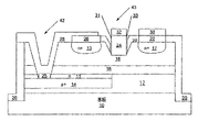
次に、図1を参照して、トランジスタ、例えば本発明の実施形態によるMESFETを詳細に説明する。図1からわかるように、基板10を設ける。基板10は、p型またはn型導電性のいずれか、あるいは半絶縁性の単結晶バルク炭化ケイ素(SiC)基板でよい。p型またはn型のいずれかの基板10は、ごく軽くドープさせることができる。基板は、6H、4H、15R、または3C炭化ケイ素を含むことができる。本明細書では、SiC基板に関して本発明を説明するが、本発明は、SiCのみに限られるものではない。例えば、いくつかの実施形態では、基板10は、本発明の範囲から逸脱することなく、例えば、ガリウム砒素(GaAs)または窒化ガリウム(GaN)を含むこともできる。
Reference is now made to FIG. 1 to describe in detail a transistor, for example a MESFET according to an embodiment of the present invention. As can be seen from FIG. 1, a
基板10上に、例えば、任意選択によるp型炭化ケイ素バッファ層12を設けることができる。このバッファ層12は、6H、4H、15R、または3Cポリタイプのp型導電炭化ケイ素で形成することができる。バッファ層12は、例えば、約0.5×1015cm-3から約3.0×1015cm-3のキャリア濃度を有することができる。適当なドーパントには、アルミニウム、ボロン、および/またはガリウムが含まれる。バッファ層12は、約2.0μmの厚さを有することができる。バッファ層12は、上記ではp型炭化ケイ素として説明しているが、本発明は、この構成のみに限られるべきものではない。代わりに、バッファ層12は、非ドープ炭化ケイ素(すなわち、意図的にドープさせない)またはごく低くドープさせたn型導電炭化ケイ素であってもよい。ごく低くドープさせたn型炭化ケイ素をバッファ層12に使用する場合、このバッファ層12のキャリア濃度は、好ましくは約5.0×1014cm-3未満である。
For example, an optional p-type silicon
図1にさらに示すように、デバイスのソース領域の下に、デバイスのドレイン領域の方に延びる端部を有するp+領域14を設ける。本明細書では、「p+」または「n+」は、同じまたは別の層または基板の、隣接するまたは他の領域に存在する領域よりも高いキャリア濃度によって画定される領域を指す。p+領域を有するトランジスタおよびその製造方法は開示されているので(特許文献7参照)、本明細書では詳細には論じないこととする。 As further shown in FIG. 1, a p + region 14 having an end extending toward the drain region of the device is provided below the source region of the device. As used herein, “p + ” or “n + ” refers to a region defined by a higher carrier concentration than a region present in an adjacent or other region of the same or another layer or substrate. Since a transistor having a p + region and a manufacturing method thereof are disclosed (see Patent Document 7), they will not be discussed in detail in this specification.
p+領域14は、p型導電領域、例えばp型導電炭化ケイ素である。p+領域14には、約1.0×1018cm-3から約1.0×1020cm-3のキャリア濃度が適し得るが、できるだけ高いキャリア濃度が好ましい。キャリア濃度は、p+領域14全体にわたって一定でなくてもよいが、p+領域14の表面では、その上にオーム接点を形成しやすいように、キャリア濃度はできるだけ高くすることが好ましい。本発明のいくつかの実施形態では、図3に示すように、基板10中にp+導電領域14を設けることができる。p+導電領域14は、例えば、バッファ層12または基板10中に約0.4μm延びることができる。ソース領域の下のp+導電領域14の存在によって、ソースからの電子注入を阻止することができ、したがって、降伏電圧の改善を実現することが可能となる。さらに、p+導電領域14はドレイン領域の下までは延びていないため、デバイス中に寄生が導入されるのを妨げることができ、したがって、デバイス性能に影響が及び得ることはない。
The p + region 14 is a p-type conductive region, for example, p-type conductive silicon carbide. A carrier concentration of about 1.0 × 10 18 cm −3 to about 1.0 × 10 20 cm −3 may be suitable for the p + region 14, but a carrier concentration as high as possible is preferred. The carrier concentration may not be constant over the entire p + region 14, but it is preferable that the carrier concentration be as high as possible on the surface of the p + region 14 so that an ohmic contact can be easily formed thereon. In some embodiments of the present invention, p +
図1にさらに示すように、p+領域14上にn型導電領域11を設ける。このn型導電領域11は、トランジスタのソース領域13の下に設け、p+領域14上を延びるが、ドレインの方に延びるp+領域14の端部を越えては延びない。言い換えれば、本発明のいくつかの実施形態では、n型導電領域11は、p+領域14上を、p+領域14の第1の端部からp+領域14の第2の端部(ドレインの方に延びる端部)まで延びることができる。本明細書では、p+領域14によってn型導電領域11の空乏化がもはや生じない場合には、n型導電領域11は、p+領域14を越えて延びる。本発明のいくつかの実施形態では、n型導電領域11は、n型導電SiC、例えば、6H、4H、15R、または3CポリタイプSiCでよい。このn型導電領域11は、バッファ層12(設ける場合)または基板10中に約500Åから約1500Å延びることができる。本発明の一実施形態では、n型導電領域11は、バッファ層12または基板10中に約1000Å未満で延びる。上記で論じたように、n型導電領域は、pn接合の固有電位(built in potential)によって実質的に空乏化し得る。したがって、実質的に空乏化したn型導電領域11によって、ソースからゲート領域の下のチャネル領域の厚さおよび導電性を選択的に増大させることができる。本発明のいくつかの実施形態では、n型導電領域11は、完全に空乏化し得る。
As further shown in FIG. 1, an n-type
本発明のいくつかの実施形態では、n型導電領域11は、ソース接点26の下から、かつ/またはn+ソース領域13の下から、ゲート電極24の第1の側壁31までさらに延びることができるが、ゲート電極24の第1の側壁31を越えては延びない。
In some embodiments of the present invention, the n-type
本発明のいくつかの実施形態では、図6に示すように、第1のp型導電領域(p+領域)14のキャリア濃度よりも低いキャリア濃度を有する第2のp型導電領域21を設けることができる。この図に示すように、第2のp型導電領域21は、第1のp型導電領域14の端部からゲート電極24の下まで延びることができ、したがって、第1および第2のp型導電領域14および21は、n型導電領域11の2つの表面に接して設けられることになる。上述したように、ゲート電極24は、第1の側壁31および第2の側壁33を有する。第1の側壁31はソース領域13に隣接し、第2の側壁33はドレイン領域17に隣接する。第2のp型導電領域21は、第1のp型導電領域14の端部からゲート電極24の第2の側壁33まで、そのゲート電極の第2の側壁を越えずに延びるか、または、第1のp型導電領域14の端部からゲート電極24の第1の側壁31と第2の側壁33との間まで延びることができる。典型的には、第2のp型導電領域21は、ゲート電極24の第1の側壁31と第2の側壁33との間のほぼ中間点まで延びる。本発明のいくつかの実施形態では、第2のp型導電領域21は、第1のp型導電領域14に自己整合させることができる。
In some embodiments of the present invention, as shown in FIG. 6, a second p-type
再び図1を参照すると、バッファ層12は、基板10と第2のバッファ層16との間に配設することができる。第2のバッファ層16は、例えば、約1.0×1015cm-3から約5×1016cm-3のキャリア濃度を有するp型炭化ケイ素とすることができる。このp型炭化ケイ素バッファ層16はまた、約1000Å未満の厚さを有することができる。本発明のいくつかの実施形態では、バッファ層16を省略することもできる。上記では、第2のバッファ層16は、p型導電炭化ケイ素として説明しているが、本発明は、この構成のみに限られるものではないことが理解されよう。代わりに、例えば、第2のバッファ層16は、バッファ層12に関して上述したように、n型導電性のものでもよく、例えば、ごく軽くドープさせたn型導電SiCまたは非ドープSiCでもよい。本発明のいくつかの実施形態では、図3に示すように、第2のバッファ層16を基板10上に直接設けることもできる。
Referring back to FIG. 1, the
図1に示すように、第2のバッファ層16上にn型導電チャネル層18を設ける。n型導電チャネル層18は、6H、4H、15R、または3Cポリタイプのn型導電炭化ケイ素で形成することができる。n型導電チャネル層は、例えば、異なるキャリア濃度を有する1つまたは複数のn型導電炭化ケイ素層を含むことができる。例えば、図4に示すように、n型導電チャネル層18は、第1のn型導電チャネル層15と、第2のn型導電チャネル層19とを含むことができる。また、n型導電チャネル層18は、n型導電SiCの第1、第2、および第3の層を含むことができる(特許文献8参照。本特許出願の開示を、参照によりその全体を記載のように本明細書に組み込む。)。
As shown in FIG. 1, an n-type
図1にさらに示すように、デバイスのソース領域およびドレイン領域をそれぞれ画定するn+領域13および17を設ける。これらのソースおよびドレイン領域13および17は、典型的にはn型導電炭化ケイ素であり、n型導電チャネル層18のキャリア濃度よりも高いキャリア濃度を有する。ソースおよびドレイン領域13および17には、約1×1019cm-3のキャリア濃度が適し得るが、できるだけ高いキャリア濃度が好ましい。
As further shown in FIG. 1, n + regions 13 and 17 are provided that define the source and drain regions of the device, respectively. These source and drain
ソースおよびドレイン注入領域13および17上にオーム接点26および22を互いに間隔を置いてそれぞれ設け、それによってソース接点26およびドレイン接点22を設ける。p+導電領域14上にオーム接点25を設けて、p+接点25を設ける。オーム接点25、26、および22は、ニッケルまたは他の適当な金属で形成することができる。p+導電領域14は、例えば、p+オーム接点25をソース接点26に電気的に結合することによって、ソース領域13と同じ電位に維持される。酸化物などの絶縁体層20をデバイスの露出表面上にさらに設けることができる。
図1にさらに示すように、第1の凹部(recess)43および接点バイアホール42を設ける。第1の凹部43を、ソース領域13とドレイン領域17との間に設ける。この第1の凹部43は、n型導電チャネル層18中に延び、n型導電チャネル層18を露出させている。接点バイアホール42を、ソース領域13に隣接して設け、n型導電領域11を貫通して延ばして、p+領域14の少なくとも一部分を露出させる。上述したように、n型導電領域11は、p+導電領域14上を、p+導電領域14の一端部から延びることができるが、ドレインの方に延びるp+導電領域14の第2の端部を越えては延びない。
As further shown in FIG. 1, a
ソース領域13とドレイン領域17との間の第1の凹部43中に、ゲート電極24を設けることができる。このゲート電極24は、クロム、プラチナ、プラチナシリサイド、ニッケル、および/またはTiWNで形成することができるが、ショットキー効果を実現するとして当業者に周知の金などの他の金属を使用することもできる。ショットキーゲート電極24は、典型的には3層構造を有する。かかる構造は、クロム(Cr)の高い接着性のため利点を有し得る。例えば、ゲート電極24は、任意選択で、n型導電チャネル層18に接触する第1のクロム(Cr)ゲート層を含むことができる。ゲート電極24は、プラチナ(Pt)および金、または他の導電性の高い金属の被覆層32をさらに含むことができる。あるいは、ゲート電極24は、第1の凹部43内のn型導電チャネル層18上に第1のニッケル層を含むことができる。ゲート電極24は、第1のニッケル層上に、金の層を含む被覆層をさらに含むことができる。
A
図1にさらに示すように、金属被覆層28、30、および32を、ソース接点26およびp+接点25、ドレイン接点22、ならびにゲート電極24上にそれぞれ設けることができる。被覆層28、30、および32は、金、銀、アルミニウム、プラチナ、および/または銅でよい。導電性の高い他の適当な金属もまた、被覆層に使用することができる。さらに、金属被覆層28によって、p+領域14のp+接点25をソース接点26に電気的に結合することができる。
As further shown in FIG. 1, metallization layers 28, 30, and 32 can be provided on
図2Aから2Hは、本発明のいくつかの実施形態によるトランジスタの製造を示す。図2Aからわかるように、基板10上に、任意選択のバッファ層12を成長または堆積させることができる。基板10は、半絶縁基板、p型基板、またはn型基板でよい。基板10は、ごく軽くドープさせることができる。基板10が半絶縁性である場合、この基板10は、開示されているように製造することができる(特許文献9参照。本特許の開示を、参照によりその全体を記載のように本明細書に組み込む。)。半絶縁基板を形成する他の技術もまた、使用することができる。バッファ層12は、約3.0×1015cm-3以下のキャリア濃度を有するp型導電炭化ケイ素でよいが、典型的には1.0×1015cm-3以下のキャリア濃度である。あるいは、バッファ層12は、n型炭化ケイ素または非ドープ(undoped)炭化ケイ素でもよい。
Figures 2A through 2H illustrate the fabrication of a transistor according to some embodiments of the present invention. As can be seen from FIG. 2A, an
図2Aにさらに示すように、p+領域14を注入するためにマスク45を形成することができる。p+領域14は、典型的には、例えば、アルミニウム、ボロン、および/またはガリウムのイオン注入によって形成される。図2Bに示すように、マスク45によって被覆されていない領域にイオン注入を実施して、p+領域14を形成する。したがって、バッファ層12が存在する場合にはその一部分に、または基板10の一部分にイオンを注入して、p型導電性の高ドープ領域、例えば、p型導電炭化ケイ素を設ける。このp型導電性の高ドープ領域は、バッファ層12または基板10中に約0.4μm延びることができる。図2Bにさらに示すように、マスク45をやはり用いて、n型導電領域11を注入することができる。n型導電領域11は、典型的には、例えば、窒素または燐のイオン注入によって形成される。図2Bに示すように、マスク45によって被覆されていない領域にイオン注入を実施して、n型導電領域11を形成することができる。n型導電領域11は、バッファ層12が存在する場合にはその中に、または基板10中に約500Åから約1500Å延びることができるが、典型的には、バッファ層12が存在する場合にはその中に、または基板10中に約1000Å未満で延びる。
As further shown in FIG. 2A, a
p型ドーパントおよびn型ドーパントの注入後、続いて高温アニールを行って注入を活性化させる。本発明のいくつかの実施形態では、n型およびp型ドーパントは、同時にアニールすることができる。適当なアニール温度は、約1300から約1600℃でよく、典型的には約1500℃である。 After the implantation of the p-type dopant and the n-type dopant, high temperature annealing is subsequently performed to activate the implantation. In some embodiments of the invention, the n-type and p-type dopants can be annealed simultaneously. A suitable annealing temperature may be about 1300 to about 1600 ° C., typically about 1500 ° C.
図2Bからわかるように、バッファ層12上に、第2のバッファ層16およびn型導電チャネル層18を成長または堆積させる。バッファ層12が含まれない場合は、基板10上に、第2のバッファ層16およびn型導電チャネル層18を成長または堆積させることができることが理解されよう。図2Bに示すように、バッファ層12上に第2のバッファ層16を形成し、第2のバッファ層16上にn型導電チャネル層18を形成する。第2のバッファ層16は、約1000Å未満の厚さを有するように形成するが、上述したように、本発明のいくつかの実施形態では省略することもできる。
As can be seen from FIG. 2B, a
図2Cに示されるように、ソース領域およびドレイン領域をそれぞれ画定するn+領域13および17を注入するために、マスク50を形成することができる。ソースおよびドレイン領域13および17は、典型的には、例えば、窒素(N)または燐(P)のイオン注入によって形成され、続いて高温アニールが行われる。適当なアニール温度は、約1100から約1600℃でよい。マスク50によって被覆されていない領域にイオン注入を実施して、図2Dに示すように、n+領域13および17を形成することができる。したがって、n型導電チャネル層18の一部分にイオンを注入して、n型導電チャネル層18よりも高いキャリア濃度を有するn型導電性の高ドープ領域、例えば、n型導電SiCを設ける。注入後、ドーパントをアニールして、注入を活性化させることができる。
As shown in FIG. 2C, a
図2Dからわかるように、基板10、バッファ層12、p+領域14、第2のバッファ層16、およびn型導電チャネル層18をエッチングして、分離メサ(isolation mesa)を形成することができる。このメサは、基板10、バッファ層12、p+領域14、第2のバッファ層16、およびn型導電チャネル層18によって画定された側壁55、57を有し、これらの側壁がトランジスタの周縁部を画定している。メサのこれらの側壁は、p+導電領域14を越えて下方に延びている。このメサは、図2Dに示されるように、デバイスの基板10中まで延びるように形成することができる。このメサは、デバイスの空乏領域を越えて延ばすことができ、それによってデバイス中の電流をメサに閉じ込め、デバイスの容量(capacitance)を低減させることができる。メサは、上述のデバイスを反応性イオンエッチングすることによって形成することができるが、当業者に周知の他の方法を用いてメサを形成することもできる。さらに、メサを使用しない場合は、陽子衝撃(proton bombardment)、補償原子(compensating atom)によるカウンタドープ(counterdoping)、または当業者に周知の他の方法などの他の方法を用いてデバイスを分離することもできる。
As can be seen in FIG. 2D, the
一実施形態では、図4に示すように、第2のバッファ層16およびn型導電チャネル層18だけをエッチングして、分離メサを形成することができる。これらの実施形態では、側壁55、57は、第2のバッファ層16およびn型導電チャネル層18によって画定され、これらの側壁がトランジスタの周縁部を画定している。本明細書で示す図は、分離メサの例示的な実施形態を示すものにすぎず、本発明の実施形態は、本明細書に示すものだけに限られるものではないことが理解されよう。例えば、分離メサは、本発明の範囲から逸脱することなく、第2のバッファ層16中まで延びていなくてもよい。
In one embodiment, as shown in FIG. 4, only the
図2Dに、MESFETの第1の凹部43の形成をさらに示す。マスク47を形成し、次いで、マスク47に従ってn型導電チャネル層18中をエッチングして第1の凹部43を形成することによって、第1の凹部43を形成することができる。第1の凹部43は、ドライまたはウェットエッチング工程などのエッチング工程によって形成することができる。例えば、第1の凹部43は、ドライエッチング、例えば、電子サイクロトロン共鳴(ECR)または誘導結合プラズマ(ICP)エッチングによって形成することができる。マスク47は、除去することができる。
FIG. 2D further illustrates the formation of the
図2Eに、第1の凹部43を上述したように形成した後の、絶縁体層20、例えば酸化物層の形成を示す。絶縁体層20は、既存の構造の露出表面上、すなわち、分離メサ、ソースおよびドレイン領域13および17、n型導電チャネル層18上、ならびに第1の凹部43中に成長または堆積させることができる。
FIG. 2E shows the formation of the
次に、図2Fを参照すると、絶縁体層20をソースおよびドレイン領域13および17まで貫通させて、接点窓をエッチングすることができる。次いで、ニッケルを蒸発させて、ソースおよびドレイン接点26および22をそれぞれ堆積させることができる。ニッケルをアニールして、図2Fに示すように、オーム接点26および22を形成することができる。かかる堆積およびアニール工程は、当業者に周知の従来の技術を使用して実施することができる。例えば、オーム接点26および22は、約950℃から約1100℃の温度で約2分間アニールすることができる。しかし、他の時間および温度も使用することができる。例えば、約30秒から約10分間の時間が許容可能となり得る。図2Fにさらに示すように、ソースおよびドレイン接点26および22の形成後、高ドープp+領域14の上方の絶縁体層20中に接点窓41をエッチングすることができる。
Next, referring to FIG. 2F, the contact layer can be etched through the
本発明のいくつかの実施形態では、オーム接点は、開示されているものと同じまたは類似の接点でよい(特許文献10参照。本特許出願の開示を、参照によりその全体を記載のように本明細書に組み込む。)。 In some embodiments of the present invention, the ohmic contact may be the same or similar to that disclosed (see US Pat. No. 6,057,096, the disclosure of which is hereby incorporated by reference in its entirety). Incorporated into the description).
図2Gに示すように、MESFETの接点バイアホール42を形成することができる。この接点バイアホール42は、MESFETの、絶縁体層20中の窓41によって画定された部分にエッチングすることができる。n型導電チャネル層18、第2のバッファ層16(存在する場合)、およびn型導電領域11を貫通してエッチングして、p+導電領域14を露出させ、それによって接点バイアホール42を形成することができる。このエッチング工程は、例えば、ドライまたはウェットエッチング工程でよい。図2Gにさらに示すように、ニッケルおよび/またはアルミニウム−チタン(AlTi)を蒸着させて、p+接点25を堆積させることができる。ニッケルをアニールして、オーム接点25を形成することができる。かかる堆積およびアニール工程は、当業者に周知の従来の技術を使用して実施することができる。例えば、オーム接点25は、約600℃から約1050℃の温度でアニールすることができる。
As shown in FIG. 2G, a contact via
図2Hに、ゲート電極24、ならびに被覆層28、30、および32の形成を示す。例えば、絶縁体20中に窓を開口し、第1の凹部43内にクロム層を堆積させることができる。典型的には、クロム層は、蒸着によって形成される。次いで、プラチナおよび金を堆積させると、ゲート構造を完成することができる。さらに示すように、ソース接点26とp+接点とは単一の被覆層28を共有しており、この被覆層28によって、ソースが高ドープp型導電領域14に電気的に結合されている。
FIG. 2H shows the formation of the
次に、図3を参照して、本発明の他の実施形態によるトランジスタの断面図について論じる。同じ番号は、先に説明した図の同じ要素を指し、したがって、これらの要素の詳細な説明は省略する。図3からわかるように、本発明のいくつかの実施形態では、基板10中にp+導電領域14およびn型導電領域を設けることができる。
Next, referring to FIG. 3, a cross-sectional view of a transistor according to another embodiment of the present invention will be discussed. The same numbers refer to the same elements of the previously described figures, and therefore a detailed description of these elements is omitted. As can be seen from FIG. 3, in some embodiments of the present invention, p +
次に図4を参照して、本発明の他の実施形態によるトランジスタの断面図について論じる。同じ番号は、先に説明した図の同じ要素を指し、したがって、これらの要素の詳細な説明は省略する。図4からわかるように、本発明のいくつかの実施形態は、単一の凹部43ではなく、二重凹部構造(double recessed structure)を含むことができる。図4に示すように、第1の凹部53用のマスクを形成し、マスクに従って第1のn型導電チャネル層19を貫通してエッチングして第1の凹部53を形成することによって、二重凹部構造の第1の凹部53を形成することができる。第1の凹部53を形成した後、絶縁層を形成することができる。図2Fに示すようにオーム接点を形成した後、第2の凹部用の第2のマスクを形成し、マスクに従って凹部をエッチングすることによって、二重凹部構造の第2の凹部54を形成することができる。第2のn型導電チャネル層15中を、例えば約600Åの距離までエッチングして、第2の凹部54を形成することができる。二重凹部構造を製造する方法はさらに開示されている(特許文献11参照)。
With reference now to FIG. 4, a cross-sectional view of a transistor according to another embodiment of the present invention will be discussed. The same numbers refer to the same elements of the previously described figures, and therefore a detailed description of these elements is omitted. As can be seen from FIG. 4, some embodiments of the present invention can include a double recessed structure rather than a
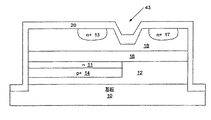
次に、図5を参照して、本発明のさらに他の実施形態によるMESFETの断面図について論じる。同じ番号は、先に説明した図の同じ要素を指し、したがって、これらの要素の説明は省略する。図5に示すように、ゲート電極24を、n型導電チャネル層18上に配設し、単一または二重凹部中には配設しない。
Next, referring to FIG. 5, a cross-sectional view of a MESFET according to still another embodiment of the present invention will be discussed. The same numbers refer to the same elements in the previously described figures, and therefore description of these elements is omitted. As shown in FIG. 5, the
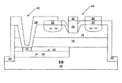
次に、図6を参照して、本発明のいくつかの実施形態によるMESFETの断面図について論じる。同じ番号は、先に説明した図の同じ要素を指し、したがって、これらの要素の説明は省略する。図6に示すように、第1のp型導電領域(p+領域)14のキャリア濃度よりも低いキャリア濃度を有する第2のp型導電領域21を設けることができる。この図でさらに示すように、第2のp型導電領域21は、第1のp型導電領域14の端部からゲート電極24の下まで延びることができ、したがって、第1および第2のp型導電領域14および21は、n型導電領域11の2つの表面に接して設けられることになる。上述したように、ゲート電極24は、第1の側壁31および第2の側壁33を有する。第1の側壁31はソース領域13に隣接し、第2の側壁33はドレイン領域17に隣接する。第2のp型導電領域21は、第1のp型導電領域14の端部からゲート電極24の第2の側壁33まで、そのゲート電極の第2の側壁を越えずに延びるか、または第1のp型導電領域14の端部からゲート電極24の第1の側壁31と第2の側壁33との間まで延びることができる。典型的には、第2のp型導電領域21は、ゲート電極24の第1の側壁31と第2の側壁33との間のほぼ中間点まで延びる。
Reference is now made to FIG. 6 to discuss cross-sectional views of MESFETs according to some embodiments of the present invention. The same numbers refer to the same elements in the previously described figures, and therefore description of these elements is omitted. As shown in FIG. 6, a second p-type
次に図7を参照して、本発明の一実施形態によるMESFETの平面図(上面図)について説明する。図7に示すように、基板10上に複数のユニットセルを設ける。ソース接点26とドレイン接点22との間にゲート電極24を配置する。図7に示すように、ソース接点26とドレイン接点22とは、相互に嵌合している。被覆層28が、接点バイアホール43中に配設されたp+接点(図示せず)を介して、ソース接点26をp+領域(図示せず)に電気的に結合している。
Next, with reference to FIG. 7, the top view (top view) of MESFET by one Embodiment of this invention is demonstrated. As shown in FIG. 7, a plurality of unit cells are provided on the
上記では、特定の層、領域、および凹部を有する特定のMESFETに関して本発明を説明しているが、本発明の実施形態は、上述のMESFETのみに限られるものではないことが理解されよう。本発明の実施形態によるソース領域下のp型およびn型導電領域は、他のタイプのトランジスタにも組み込むことができる。例えば、本発明の実施形態によるp型導電領域は、他のMESFETに組み込むことができる(特許文献12参照。本特許の開示を、参照によりその全体を記載のように本明細書に組み込む。)。 While the invention has been described above with respect to particular MESFETs having particular layers, regions, and recesses, it will be understood that embodiments of the invention are not limited to the MESFETs described above. The p-type and n-type conductive regions under the source region according to embodiments of the present invention can be incorporated into other types of transistors. For example, a p-type conductive region according to embodiments of the present invention can be incorporated into other MESFETs (see US Pat. No. 6,057,071; the disclosure of this patent is incorporated herein by reference in its entirety). .
上記では、SiC MESFETに関して本発明を説明しているが、本発明は、SiC MESFETのみに限られるものではない。例えば、本発明の実施形態によるMESFETは、例えばガリウム砒素(GaAs)MESFET、または窒化ガリウム(GaN)MESFETであってもよい。特に、GaAs MESFETに関して本発明を説明した場合には、p型導電領域は、p型導電GaAs領域となり、n型導電チャネル層は、n型導電GaAs層などになったであろう。さらに、本発明のいくつかの実施形態によるMESFETは、例えば、SiC MESFET MMIC、GaN HEMT、GaN HEMT MMIC、GaAs MESFET、GaAs MESFET MMIC、GaAs HEMT、GaAs HEMT MMIC、GaAs pHEMT、GaAs pHEMT MMICなどであってもよい。 Although the present invention has been described above with respect to SiC MESFETs, the present invention is not limited to SiC MESFETs. For example, a MESFET according to embodiments of the present invention may be, for example, a gallium arsenide (GaAs) MESFET or a gallium nitride (GaN) MESFET. In particular, when the present invention was described with respect to a GaAs MESFET, the p-type conductive region would have become a p-type conductive GaAs region and the n-type conductive channel layer would have become an n-type conductive GaAs layer or the like. Further, the MESFETs according to some embodiments of the present invention are, for example, SiC MESFET MMIC, GaN HEMT, GaN HEMT MMIC, GaAs MESFET, GaAs MESFET MMIC, GaAs HEMT, GaAs HEMT MMIC, GaAs pHEMT, GaAs pHEMT MMIC, and the like. May be.
図面および明細書では、本発明の典型的な好ましい実例形態を開示し、特定の用語を使用してきたが、これらは概括的かつ説明的な意味で使用したものにすぎず、添付の特許請求の範囲に記載の本発明の範囲を限定するものではない。 In the drawings and specification, there have been disclosed typical preferred embodiments of the present invention, and specific language has been used, but these have been used in a generic and descriptive sense only, and are not limited to the accompanying claims. It is not intended to limit the scope of the invention described in the scope.
Claims (45)
前記ソース領域の下にあり、前記ドレイン領域の方に延びる端部を有するp型導電領域であって、前記n型導電チャネル層から間隔を置いて配置され、前記ソース領域に電気的に結合され、隣接する領域よりも高いキャリア濃度を有する前記p型導電領域と、
前記ソース領域の下の前記p型導電領域上にあり、前記ドレイン領域の方に、前記p型導電領域の前記端部まで延びるn型導電領域とを備え、
前記ゲート電極は、第1の側壁および第2の側壁を有し、前記第1の側壁が前記ソース領域に隣接し、前記第2の側壁が前記ドレイン領域に隣接し、
前記n型導電領域は、前記ソース領域の下から前記ゲート電極の前記第1の側壁の方に延びるが、前記ゲート電極の前記第1の側壁を越えては延びず、前記p型導電領域との接合によって空乏化し、前記n型導電チャネル層の空乏化が生じる可能性を低減することを特徴とする金属半導体電界効果トランジスタ(MESFET)のユニットセル。A MESFET having a source region, a drain region, and a gate electrode , wherein the gate electrode is on an n-type conductive channel layer between the source region and the drain region;
A p-type conductive region under the source region and having an end extending toward the drain region, spaced from the n-type conductive channel layer and electrically coupled to the source region , said p-type conductive region that have a higher carrier concentration than the adjacent region,
Wherein it is in the p-type conductivity region beneath the source region, toward the drain region, and a n-type conductive region Ru extends to the end of the p-type conductive region,
The gate electrode has a first sidewall and a second sidewall, the first sidewall is adjacent to the source region, the second sidewall is adjacent to the drain region,
The n-type conductive region is extending from the bottom of the source region towards said first sidewall of said gate electrode, over the first sidewall of the gate electrode not extend, said p-type conductive region A unit cell of a metal semiconductor field effect transistor (MESFET), characterized in that the possibility of depletion of the n-type conductive channel layer due to depletion of the junction is reduced .
前記ソース領域の下にあり、前記ドレイン領域の方に延びる端部を有し、前記n型導電チャネル層から間隔を置いて配置され、前記ソース領域に電気的に結合され、隣接する領域よりも高いキャリア濃度を有するp型導電領域であって、前記ゲート電極の第1の側壁の方に延びるが前記ゲート電極の第1の側壁を越えては延びない第1のp型導電領域と、前記第1のp型導電領域のキャリア濃度よりも低いキャリア濃度を有し、前記第1のp型導電領域の端部から前記ゲート電極の下まで延びる第2のp型導電領域とを備える前記p型導電領域と、
前記ソース領域の下の前記第1のp型導電領域上にあり、前記ドレイン領域の方に、前記第1のp型導電領域の端部まで延びるn型導電領域とを備え、
前記ゲート電極が、第1の側壁および第2の側壁を有し、前記第1の側壁が前記ソース領域に隣接し、前記第2の側壁が前記ドレイン領域に隣接し、
前記第1のp型導電領域が、前記n型導電領域の下面に接し、前記第2のp型導電領域が、前記n型導電領域の側面に接して設けられ、
前記n型導電領域は、前記ソース領域の下から前記ゲート電極の前記第1の側壁の方に延びるが、前記ゲート電極の前記第1の側壁を越えては延びず、前記p型導電領域との接合によって空乏化し、前記n型導電チャネル層の空乏化が生じる可能性を低減することを特徴とする金属半導体電界効果トランジスタ(MESFET)のユニットセル。A MESFET having a source region, a drain region, and a gate electrode, wherein the gate electrode is on an n-type conductive channel layer between the source region and the drain region;
Located under the source region, it has a end portion extending toward said drain region, spaced apart from said n-type conductivity channel layer, is electrically coupled to the source region, than adjacent regions A p-type conductive region having a high carrier concentration, the first p-type conductive region extending toward the first side wall of the gate electrode but not extending beyond the first side wall of the gate electrode; A second p-type conductive region having a carrier concentration lower than that of the first p-type conductive region and extending from an end of the first p-type conductive region to below the gate electrode; Type conductive region ;
Wherein below the source region is in the first p-type conductivity region, towards the drain region, and a first p-type conductivity region n-type conductive region Ru extending to the end of,
The gate electrode has a first sidewall and a second sidewall; the first sidewall is adjacent to the source region; the second sidewall is adjacent to the drain region;
The first p-type conductive region is in contact with the lower surface of the n-type conductive region, and the second p-type conductive region is provided in contact with a side surface of the n-type conductive region;
The n-type conductive region extends from below the source region toward the first sidewall of the gate electrode, but does not extend beyond the first sidewall of the gate electrode, and the p-type conductive region A unit cell of a metal semiconductor field effect transistor (MESFET), characterized in that the possibility of depletion of the n-type conductive channel layer due to depletion of the junction is reduced.
前記ソース領域の下にあり、前記ドレイン領域の方に延びる端部を有するp型導電領域であって、前記n型導電チャネル層から間隔を置いて配置され、前記ソース領域に電気的に結合され、隣接する領域よりも高いキャリア濃度を有する前記p型導電領域と、
前記ソース領域の下の前記p型導電領域上にあり、前記ドレイン領域の方に、前記p型導電領域の前記端部まで延びるn型導電領域と、
前記ソース領域に隣接し、前記p型導電領域を露出させる接点バイアホールとを備え、
前記ゲート電極が、第1の側壁および第2の側壁を有し、前記第1の側壁が前記ソース領域に隣接し、前記第2の側壁が前記ドレイン領域に隣接し、
前記n型導電領域が、前記p型導電領域の前記露出部分から前記ゲート電極の前記第1の側壁の方に延びるが、前記ゲート電極の前記第1の側壁を越えては延びず、前記p型導電領域との接合によって空乏化し、前記n型導電チャネル層の空乏化が生じる可能性を低減することを特徴とする金属半導体電界効果トランジスタ(MESFET)のユニットセル。A MESFET having a source region, a drain region, and a gate electrode , wherein the gate electrode is on an n-type conductive channel layer between the source region and the drain region;
A p-type conductive region under the source region and having an end extending toward the drain region, spaced from the n-type conductive channel layer and electrically coupled to the source region , said p-type conductive region that have a higher carrier concentration than the adjacent region,
Said located on the p-type conductivity region beneath the source region, the towards the drain region, n-type conductive region Ru extends to the end of the p-type conductive region,
A contact via hole adjacent to the source region and exposing the p-type conductive region;
The gate electrode has a first sidewall and a second sidewall; the first sidewall is adjacent to the source region; the second sidewall is adjacent to the drain region;
The n-type conductive region extends from the exposed portion of the p-type conductive region toward the first sidewall of the gate electrode, but does not extend beyond the first sidewall of the gate electrode , and the p A unit cell of a metal semiconductor field effect transistor (MESFET), characterized in that the possibility of depletion of the n-type conductive channel layer caused by depletion by a junction with a type conductive region is reduced .
前記ソース領域の下にあり、前記ドレイン領域の方に延びる端部を有するp型導電SiC領域であって、前記n型導電SiCチャネル層から間隔を置いて配置され、前記ソース領域に電気的に結合され、隣接する領域よりも高いキャリア濃度を有する前記p型導電SiC領域と、
前記ソース領域の下の前記p型導電SiC領域上にあり、前記ドレイン領域の方に、前記p型導電SiC領域の前記端部まで延びるn型導電SiC領域とを備え、
前記ゲート電極は、第1の側壁および第2の側壁を有し、前記第1の側壁が前記ソース領域に隣接し、前記第2の側壁が前記ドレイン領域に隣接し、
前記n型導電SiC領域は、前記ソース領域の下から前記ゲート電極の前記第1の側壁の方に延びるが、前記ゲート電極の前記第1の側壁を越えては延びず、前記p型導電SiC領域との接合によって空乏化し、前記n型導電SiCチャネル層の空乏化が生じる可能性を低減することを特徴とする金属半導体電界効果トランジスタ(MESFET)のユニットセル。A silicon carbide (SiC) MESFET having a source region, a drain region, and a gate electrode , wherein the gate electrode is on an n-type conductive SiC channel layer between the source region and the drain region;
A p-type conductive SiC region under the source region and having an end extending toward the drain region, spaced from the n-type conductive SiC channel layer and electrically connected to the source region; coupled, with the p-type conductivity SiC region that have a higher carrier concentration than the adjacent region,
The is on the p-type conductivity SiC region under the source region, toward the drain region, and a said p-type conductivity n-type conductivity SiC region Ru extending to said end of SiC region,
The gate electrode has a first sidewall and a second sidewall, the first sidewall is adjacent to the source region, the second sidewall is adjacent to the drain region,
Wherein n-type conductivity SiC region is extending from the bottom of the source region towards said first sidewall of said gate electrode, not extend beyond the first sidewall of the gate electrode, the p-type conductivity SiC A unit cell of a metal semiconductor field effect transistor (MESFET), characterized in that the possibility of depletion of the n-type conductive SiC channel layer by depletion due to junction with a region is reduced .
前記ソース領域の下にあり、前記ドレイン領域の方に延びる端部を有するp型導電領域であって、前記n型導電チャネル層から間隔を置いて配置され、前記ソース領域に電気的に結合され、隣接する領域よりも高いキャリア濃度を有する前記p型導電領域を形成すること、および、
前記ソース領域の下の前記p型導電領域上にあり、前記ドレイン領域の方に、前記p型導電領域の前記端部まで延びるn型導電領域を形成することを含み、
前記ゲート電極は、第1の側壁および第2の側壁を有し、前記第1の側壁が前記ソース領域に隣接し、前記第2の側壁が前記ドレイン領域に隣接し、
前記n型導電領域を形成することは、前記ソース領域の下から前記ゲート電極の前記第1の側壁の方に延びるが、前記ゲート電極の前記第1の側壁を越えては延びず、前記p型導電領域との接合によって空乏化し、前記n型導電チャネル層の空乏化が生じる可能性を低減する前記n型導電領域を形成すること含むことを特徴とする金属半導体電界効果トランジスタ(MESFET)を形成する方法。Forming a MESFET having a source region, a drain region, and a gate electrode , wherein the gate electrode is on an n-type conductive channel layer between the source region and the drain region;
A p-type conductive region under the source region and having an end extending toward the drain region, spaced from the n-type conductive channel layer and electrically coupled to the source region , wherein forming the p-type conductive region that have a higher carrier concentration than the adjacent regions, and,
Wherein is in the p-type conductivity region beneath the source region, toward the drain region includes forming an n-type conductive region Ru extends to the end of the p-type conductive region,
The gate electrode has a first sidewall and a second sidewall, the first sidewall is adjacent to the source region, the second sidewall is adjacent to the drain region,
Wherein forming the n-type conductive region is extending from the bottom of the source region towards said first sidewall of said gate electrode, not extend beyond the first sidewall of the gate electrode, the p Forming a metal semiconductor field effect transistor (MESFET), comprising forming the n-type conductive region which is depleted by junction with the type-conductive region and reduces the possibility of depletion of the n-type conductive channel layer How to form.
前記ソースおよびドレイン領域上に第1および第2のオーム接点をそれぞれ形成することをさらに含むことを特徴とする請求項20に記載の方法。Forming an n-type conductive SiC implantation region in the n-type conductive channel layer defining the source region and the drain region having a carrier concentration higher than that of the n-type conductive channel layer; and
21. The method of claim 20 , further comprising forming first and second ohmic contacts on the source and drain regions, respectively.
前記ソース領域の下にあり、前記ドレイン領域の方に延びる端部を有し、前記n型導電チャネル層から間隔を置いて配置され、前記ソース領域に電気的に結合され、隣接する領域よりも高いキャリア濃度を有するp型導電領域であって、前記ゲート電極の第1の側壁の方に延びるが前記ゲート電極の第1の側壁を越えては延びない第1のp型導電領域と、前記第1のp型導電領域のキャリア濃度よりも低いキャリア濃度を有し、前記第1のp型導電領域の端部から前記ゲート電極の下まで延びる第2のp型導電領域とを備える前記p型導電領域を形成すること、および、
前記ソース領域の下の前記第1のp型導電領域上にあり、前記ドレイン領域の方に、前記第1のp型導電領域の端部まで延びるn型導電領域を形成することを含むことを特徴とする金属半導体電界効果トランジスタ(MESFET)を形成する方法であって、
前記ゲート電極が、第1の側壁および第2の側壁を有し、前記第1の側壁が前記ソース領域に隣接し、前記第2の側壁が前記ドレイン領域に隣接し、
前記第1のp型導電領域が、前記n型導電領域の下面に接し、前記第2のp型導電領域が、前記n型導電領域の側面に接して設けられることを含み、
前記n型導電領域は、前記ソース領域の下から前記ゲート電極の前記第1の側壁の方に延びるが、前記ゲート電極の前記第1の側壁を越えては延びず、前記p型導電領域との接合によって空乏化し、前記n型導電チャネル層の空乏化が生じる可能性を低減することを特徴とする金属半導体電界効果トランジスタ(MESFET)を形成する方法。Forming a MESFET having a source region, a drain region, and a gate electrode, wherein the gate electrode is on an n-type conductive channel layer between the source region and the drain region;
Located under the source region, it has a end portion extending toward said drain region, spaced apart from said n-type conductivity channel layer, is electrically coupled to the source region, than adjacent regions A p-type conductive region having a high carrier concentration, the first p-type conductive region extending toward the first side wall of the gate electrode but not extending beyond the first side wall of the gate electrode; A second p-type conductive region having a carrier concentration lower than that of the first p-type conductive region and extending from an end of the first p-type conductive region to below the gate electrode; Forming a mold conductive region ; and
Wherein below the source region is in the first p-type conductivity region, towards the drain region, that includes forming a n-type conductive region Ru extends to an end portion of the first p-type conductivity region A method of forming a metal semiconductor field effect transistor (MESFET) characterized by comprising:
The gate electrode has a first sidewall and a second sidewall; the first sidewall is adjacent to the source region; the second sidewall is adjacent to the drain region;
The first p-type conductive region is provided in contact with the lower surface of the n-type conductive region, and the second p-type conductive region is provided in contact with a side surface of the n-type conductive region,
The n-type conductive region extends from below the source region toward the first sidewall of the gate electrode, but does not extend beyond the first sidewall of the gate electrode, and the p-type conductive region A method of forming a metal semiconductor field effect transistor (MESFET), characterized in that the possibility of depletion of the n-type conductive channel layer is reduced by depletion of the junction.
前記ソース領域の下にあり、前記ドレイン領域の方に延びる端部を有するp型導電領域であって、前記n型導電チャネル層から間隔を置いて配置され、前記ソース領域に電気的に結合され、隣接する領域よりも高いキャリア濃度を有する前記p型導電領域を形成すること、
前記ソース領域の下の前記p型導電領域上にあり、前記ドレイン領域の方に、前記p型導電領域の前記端部まで延びるn型導電領域を形成すること、および、
前記ソース領域に隣接し、前記p型導電領域を露出させる接点バイアホールを形成することを含み、
前記ゲート電極が、第1の側壁および第2の側壁を有し、前記第1の側壁が前記ソース領域に隣接し、前記第2の側壁が前記ドレイン領域に隣接し、
前記n型導電領域が、前記p型導電領域の前記露出部分から前記ゲート電極の前記第1の側壁の方に延びるが、前記ゲート電極の前記第1の側壁を越えては延びず、前記p型導電領域との接合によって空乏化し、前記n型導電チャネル層の空乏化が生じる可能性を低減することを特徴とする金属半導体電界効果トランジスタ(MESFET)を形成する方法。Forming a MESFET having a source region, a drain region, and a gate electrode , wherein the gate electrode is on an n-type conductive channel layer between the source region and the drain region;
A p-type conductive region under the source region and having an end extending toward the drain region, spaced from the n-type conductive channel layer and electrically coupled to the source region , wherein forming the p-type conductive region that have a higher carrier concentration than the adjacent region,
Wherein is in the p-type conductivity region beneath the source region, the towards the drain region, forming a n-type conductive region Ru extends to the end of the p-type conductive region, and,
Forming a contact via hole adjacent to the source region and exposing the p-type conductive region;
The gate electrode has a first sidewall and a second sidewall; the first sidewall is adjacent to the source region; the second sidewall is adjacent to the drain region;
The n-type conductive region extends from the exposed portion of the p-type conductive region toward the first sidewall of the gate electrode, but does not extend beyond the first sidewall of the gate electrode , and the p A method of forming a metal semiconductor field effect transistor (MESFET), characterized in that the possibility of depletion of the n-type conductive channel layer is reduced by depletion by a junction with a type conductive region .
前記ソース領域の下にあり、前記ドレイン領域の方に延びる端部を有するp型導電領域であって、前記n型導電チャネル層から間隔を置いて配置され、前記ソース領域に電気的に結合され、隣接する領域よりも高いキャリア濃度を有する前記p型導電領域と、
前記ソース領域の下の前記p型導電領域上にあり、前記ドレイン領域の方に、前記p型導電領域の前記端部まで延びるn型導電領域と、
前記ソース領域に隣接し、前記p型導電領域を露出させるバイアホールとを備え、
前記ゲート電極が、第1の側壁および第2の側壁を有し、前記第1の側壁が前記ソース領域に隣接し、前記第2の側壁が前記ドレイン領域に隣接し、
前記n型導電領域は、前記p型導電領域の前記露出部分から前記ゲート電極の前記第1の側壁の方に延びるが、前記ゲート電極の前記第1の側壁を越えては延びず、前記p型導電領域との接合によって空乏化し、前記n型導電チャネル層の空乏化が生じる可能性を低減することを特徴とする金属半導体電界効果トランジスタ(MESFET)のユニットセル。A MESFET having a source region, a drain region, and a gate electrode , wherein the gate electrode is on an n-type conductive channel layer between the source region and the drain region;
A p-type conductive region under the source region and having an end extending toward the drain region, spaced from the n-type conductive channel layer and electrically coupled to the source region , said p-type conductive region that have a higher carrier concentration than the adjacent region,
Said located on the p-type conductivity region beneath the source region, the towards the drain region, n-type conductive region Ru extends to the end of the p-type conductive region,
A via hole adjacent to the source region and exposing the p-type conductive region;
The gate electrode has a first sidewall and a second sidewall; the first sidewall is adjacent to the source region; the second sidewall is adjacent to the drain region;
The n-type conductive region extends from the exposed portion of the p-type conductive region toward the first sidewall of the gate electrode, but does not extend beyond the first sidewall of the gate electrode. A unit cell of a metal semiconductor field effect transistor (MESFET) , characterized in that the possibility of depletion of the n-type conductive channel layer caused by depletion by a junction with a type conductive region is reduced .
Applications Claiming Priority (2)
| Application Number | Priority Date | Filing Date | Title |
|---|---|---|---|
| US11/012,553 US7326962B2 (en) | 2004-12-15 | 2004-12-15 | Transistors having buried N-type and P-type regions beneath the source region and methods of fabricating the same |
| PCT/US2005/035505 WO2006065324A2 (en) | 2004-12-15 | 2005-10-04 | Transistors having buried n-type and p-type regions beneath the source region and methods of fabricating the same |
Publications (3)
| Publication Number | Publication Date |
|---|---|
| JP2008524843A JP2008524843A (en) | 2008-07-10 |
| JP2008524843A5 JP2008524843A5 (en) | 2008-08-21 |
| JP4335283B2 true JP4335283B2 (en) | 2009-09-30 |
Family
ID=36582806
Family Applications (1)
| Application Number | Title | Priority Date | Filing Date |
|---|---|---|---|
| JP2007546650A Active JP4335283B2 (en) | 2004-12-15 | 2005-10-04 | Transistor having buried n-type and p-type regions under source region, and method for manufacturing the same |
Country Status (8)
| Country | Link |
|---|---|
| US (1) | US7326962B2 (en) |
| EP (1) | EP1825517B1 (en) |
| JP (1) | JP4335283B2 (en) |
| KR (1) | KR101121600B1 (en) |
| AT (1) | ATE428187T1 (en) |
| CA (1) | CA2590626C (en) |
| DE (1) | DE602005013815D1 (en) |
| WO (1) | WO2006065324A2 (en) |
Families Citing this family (16)
| Publication number | Priority date | Publication date | Assignee | Title |
|---|---|---|---|---|
| JP5261923B2 (en) * | 2006-10-17 | 2013-08-14 | サンケン電気株式会社 | Compound semiconductor device |
| JP5114947B2 (en) * | 2006-12-28 | 2013-01-09 | 富士通株式会社 | Nitride semiconductor device and manufacturing method thereof |
| JP5564842B2 (en) | 2009-07-10 | 2014-08-06 | サンケン電気株式会社 | Semiconductor device |
| JP5397289B2 (en) | 2010-03-29 | 2014-01-22 | 住友電気工業株式会社 | Field effect transistor |
| JP5879694B2 (en) * | 2011-02-23 | 2016-03-08 | ソニー株式会社 | Field effect transistor, semiconductor switch circuit, and communication device |
| US8476979B1 (en) | 2011-07-07 | 2013-07-02 | The United States Of America As Represented By The Administrator Of National Aeronautics And Space Administration | High-efficiency power module |
| US9024356B2 (en) * | 2011-12-20 | 2015-05-05 | Infineon Technologies Austria Ag | Compound semiconductor device with buried field plate |
| US10164038B2 (en) * | 2013-01-30 | 2018-12-25 | Taiwan Semiconductor Manufacturing Company, Ltd. | Method of implanting dopants into a group III-nitride structure and device formed |
| US9385224B2 (en) * | 2014-08-13 | 2016-07-05 | Northrop Grumman Systems Corporation | Method of forming an integrated multichannel device and single channel device structure |
| US10192980B2 (en) | 2016-06-24 | 2019-01-29 | Cree, Inc. | Gallium nitride high-electron mobility transistors with deep implanted p-type layers in silicon carbide substrates for power switching and radio frequency applications and process for making the same |
| US11430882B2 (en) * | 2016-06-24 | 2022-08-30 | Wolfspeed, Inc. | Gallium nitride high-electron mobility transistors with p-type layers and process for making the same |
| US10892356B2 (en) | 2016-06-24 | 2021-01-12 | Cree, Inc. | Group III-nitride high-electron mobility transistors with buried p-type layers and process for making the same |
| US10840334B2 (en) | 2016-06-24 | 2020-11-17 | Cree, Inc. | Gallium nitride high-electron mobility transistors with deep implanted p-type layers in silicon carbide substrates for power switching and radio frequency applications and process for making the same |
| KR102381395B1 (en) * | 2017-09-18 | 2022-04-01 | 한국전기연구원 | Implementation of SiC Semiconductor Devices On 6H-SiC Insulation or Semi-insulation Substrate And Manufacturing Methods of The Same |
| US11929428B2 (en) | 2021-05-17 | 2024-03-12 | Wolfspeed, Inc. | Circuits and group III-nitride high-electron mobility transistors with buried p-type layers improving overload recovery and process for implementing the same |
| US20230078017A1 (en) * | 2021-09-16 | 2023-03-16 | Wolfspeed, Inc. | Semiconductor device incorporating a substrate recess |
Family Cites Families (50)
| Publication number | Priority date | Publication date | Assignee | Title |
|---|---|---|---|---|
| JPS51424Y2 (en) | 1971-02-02 | 1976-01-08 | ||
| DE2324780C3 (en) * | 1973-05-16 | 1978-07-27 | Siemens Ag, 1000 Berlin Und 8000 Muenchen | Method for manufacturing a semiconductor component |
| JPS6051213B2 (en) | 1978-05-30 | 1985-11-13 | 株式会社フジクラ | Manufacturing equipment for flexible tape electric wire |
| JPS59134874A (en) | 1983-01-21 | 1984-08-02 | Hitachi Ltd | Semiconductor device |
| US4762806A (en) * | 1983-12-23 | 1988-08-09 | Sharp Kabushiki Kaisha | Process for producing a SiC semiconductor device |
| JPS60142568A (en) | 1983-12-29 | 1985-07-27 | Sharp Corp | Manufacture of sic field effect transistor |
| US4737469A (en) * | 1984-01-19 | 1988-04-12 | Honeywell Inc. | Controlled mode field effect transistors and method therefore |
| JPS60154674A (en) | 1984-01-25 | 1985-08-14 | Hitachi Ltd | Manufacture of electronic device |
| JPS60189250A (en) | 1984-03-08 | 1985-09-26 | Fujitsu Ltd | Semiconductor device |
| DE3578271D1 (en) * | 1984-11-02 | 1990-07-19 | Toshiba Kawasaki Kk | FIELD EFFECT TRANSISTOR WITH A SCHOTTKY GATE AND MANUFACTURING METHOD DAFUER. |
| JP2615390B2 (en) * | 1985-10-07 | 1997-05-28 | 工業技術院長 | Method of manufacturing silicon carbide field effect transistor |
| EP0252179B1 (en) * | 1986-07-11 | 1992-05-27 | International Business Machines Corporation | Process for producing undercut mask profiles |
| US5229625A (en) * | 1986-08-18 | 1993-07-20 | Sharp Kabushiki Kaisha | Schottky barrier gate type field effect transistor |
| JPS6347983A (en) | 1986-08-18 | 1988-02-29 | Sharp Corp | Silicon carbide field effect transistor |
| JPS6459961A (en) | 1987-08-31 | 1989-03-07 | Toshiba Corp | Semiconductor device |
| JPH0797659B2 (en) | 1987-10-20 | 1995-10-18 | 三洋電機株式会社 | SiC blue light emitting diode |
| US4947218A (en) * | 1987-11-03 | 1990-08-07 | North Carolina State University | P-N junction diodes in silicon carbide |
| JPH0798684B2 (en) | 1988-01-19 | 1995-10-25 | 日本碍子株式会社 | Method for manufacturing high density SiC sintered body |
| JPH01196873A (en) | 1988-02-02 | 1989-08-08 | Sharp Corp | Silicon carbide semiconductor device |
| JP2612040B2 (en) | 1988-06-28 | 1997-05-21 | 株式会社豊田中央研究所 | MOS-FET using β-SiC and manufacturing method thereof |
| US5014108A (en) * | 1990-05-15 | 1991-05-07 | Harris Corporation | MESFET for dielectrically isolated integrated circuits |
| JPH04225534A (en) | 1990-12-27 | 1992-08-14 | Fujitsu Ltd | Semiconductor device and manufacture thereof |
| JPH0547798A (en) * | 1991-01-31 | 1993-02-26 | Texas Instr Inc <Ti> | Gaas fet with resistive a1gaas |
| US5289015A (en) * | 1991-04-25 | 1994-02-22 | At&T Bell Laboratories | Planar fet-seed integrated circuits |
| US5264713A (en) * | 1991-06-14 | 1993-11-23 | Cree Research, Inc. | Junction field-effect transistor formed in silicon carbide |
| US5270554A (en) | 1991-06-14 | 1993-12-14 | Cree Research, Inc. | High power high frequency metal-semiconductor field-effect transistor formed in silicon carbide |
| US5925895A (en) * | 1993-10-18 | 1999-07-20 | Northrop Grumman Corporation | Silicon carbide power MESFET with surface effect supressive layer |
| US5510630A (en) * | 1993-10-18 | 1996-04-23 | Westinghouse Electric Corporation | Non-volatile random access memory cell constructed of silicon carbide |
| US5396085A (en) * | 1993-12-28 | 1995-03-07 | North Carolina State University | Silicon carbide switching device with rectifying-gate |
| US5399883A (en) * | 1994-05-04 | 1995-03-21 | North Carolina State University At Raleigh | High voltage silicon carbide MESFETs and methods of fabricating same |
| US5686737A (en) * | 1994-09-16 | 1997-11-11 | Cree Research, Inc. | Self-aligned field-effect transistor for high frequency applications |
| SE9404452D0 (en) * | 1994-12-22 | 1994-12-22 | Abb Research Ltd | Semiconductor device having an insulated gate |
| JP3158973B2 (en) | 1995-07-20 | 2001-04-23 | 富士電機株式会社 | Silicon carbide vertical FET |
| US5972801A (en) * | 1995-11-08 | 1999-10-26 | Cree Research, Inc. | Process for reducing defects in oxide layers on silicon carbide |
| JP2728126B2 (en) * | 1995-12-25 | 1998-03-18 | 日本電気株式会社 | Field effect transistor |
| US5719409A (en) * | 1996-06-06 | 1998-02-17 | Cree Research, Inc. | Silicon carbide metal-insulator semiconductor field effect transistor |
| DE19644821C1 (en) | 1996-10-29 | 1998-02-12 | Daimler Benz Ag | Controllable semiconductor structure for use instead of JFET, MESFET |
| US5742082A (en) * | 1996-11-22 | 1998-04-21 | Motorola, Inc. | Stable FET with shielding region in the substrate |
| US5891769A (en) * | 1997-04-07 | 1999-04-06 | Motorola, Inc. | Method for forming a semiconductor device having a heteroepitaxial layer |
| US6121633A (en) * | 1997-06-12 | 2000-09-19 | Cree Research, Inc. | Latch-up free power MOS-bipolar transistor |
| JPH11150124A (en) | 1997-09-12 | 1999-06-02 | Toshiba Corp | Field effect transistor and its manufacture |
| JP3216804B2 (en) | 1998-01-06 | 2001-10-09 | 富士電機株式会社 | Manufacturing method of silicon carbide vertical FET and silicon carbide vertical FET |
| US6107649A (en) * | 1998-06-10 | 2000-08-22 | Rutgers, The State University | Field-controlled high-power semiconductor devices |
| US6316793B1 (en) * | 1998-06-12 | 2001-11-13 | Cree, Inc. | Nitride based transistors on semi-insulating silicon carbide substrates |
| US6218680B1 (en) * | 1999-05-18 | 2001-04-17 | Cree, Inc. | Semi-insulating silicon carbide without vanadium domination |
| US6686616B1 (en) | 2000-05-10 | 2004-02-03 | Cree, Inc. | Silicon carbide metal-semiconductor field effect transistors |
| JP2002252233A (en) * | 2001-02-22 | 2002-09-06 | Matsushita Electric Ind Co Ltd | Semiconductor device and method of manufacturing the same |
| US6458640B1 (en) * | 2001-06-04 | 2002-10-01 | Anadigics, Inc. | GaAs MESFET having LDD and non-uniform P-well doping profiles |
| US6906350B2 (en) * | 2001-10-24 | 2005-06-14 | Cree, Inc. | Delta doped silicon carbide metal-semiconductor field effect transistors having a gate disposed in a double recess structure |
| US6956239B2 (en) * | 2002-11-26 | 2005-10-18 | Cree, Inc. | Transistors having buried p-type layers beneath the source region |
-
2004
- 2004-12-15 US US11/012,553 patent/US7326962B2/en active Active
-
2005
- 2005-10-04 CA CA2590626A patent/CA2590626C/en active Active
- 2005-10-04 KR KR1020077015942A patent/KR101121600B1/en active IP Right Grant
- 2005-10-04 DE DE602005013815T patent/DE602005013815D1/en active Active
- 2005-10-04 AT AT05803118T patent/ATE428187T1/en not_active IP Right Cessation
- 2005-10-04 JP JP2007546650A patent/JP4335283B2/en active Active
- 2005-10-04 EP EP05803118A patent/EP1825517B1/en active Active
- 2005-10-04 WO PCT/US2005/035505 patent/WO2006065324A2/en active Application Filing
Also Published As
| Publication number | Publication date |
|---|---|
| JP2008524843A (en) | 2008-07-10 |
| US7326962B2 (en) | 2008-02-05 |
| WO2006065324A2 (en) | 2006-06-22 |
| KR101121600B1 (en) | 2012-02-28 |
| WO2006065324A3 (en) | 2006-10-19 |
| EP1825517A2 (en) | 2007-08-29 |
| CA2590626A1 (en) | 2006-06-22 |
| KR20070087046A (en) | 2007-08-27 |
| EP1825517B1 (en) | 2009-04-08 |
| CA2590626C (en) | 2014-04-08 |
| US20060125001A1 (en) | 2006-06-15 |
| ATE428187T1 (en) | 2009-04-15 |
| DE602005013815D1 (en) | 2009-05-20 |
Similar Documents
| Publication | Publication Date | Title |
|---|---|---|
| JP4335283B2 (en) | Transistor having buried n-type and p-type regions under source region, and method for manufacturing the same | |
| JP5758796B2 (en) | Transistor having p-type buried layer under source region and method for manufacturing the same | |
| US7348612B2 (en) | Metal-semiconductor field effect transistors (MESFETs) having drains coupled to the substrate and methods of fabricating the same | |
| TWI385799B (en) | Asymmetric layout structures for transistors and methods of fabricating the same | |
| US6906350B2 (en) | Delta doped silicon carbide metal-semiconductor field effect transistors having a gate disposed in a double recess structure | |
| WO2005122256A2 (en) | Voltage booster transistor | |
| WO2005122398A2 (en) | Lateral drift vertical metal-insulator semiconductors | |
| US7402844B2 (en) | Metal semiconductor field effect transistors (MESFETS) having channels of varying thicknesses and related methods | |
| US7880172B2 (en) | Transistors having implanted channels and implanted P-type regions beneath the source region |
Legal Events
| Date | Code | Title | Description |
|---|---|---|---|
| A521 | Request for written amendment filed |
Free format text: JAPANESE INTERMEDIATE CODE: A523 Effective date: 20080630 |
|
| A621 | Written request for application examination |
Free format text: JAPANESE INTERMEDIATE CODE: A621 Effective date: 20080630 |
|
| A871 | Explanation of circumstances concerning accelerated examination |
Free format text: JAPANESE INTERMEDIATE CODE: A871 Effective date: 20080630 |
|
| A975 | Report on accelerated examination |
Free format text: JAPANESE INTERMEDIATE CODE: A971005 Effective date: 20080801 |
|
| A131 | Notification of reasons for refusal |
Free format text: JAPANESE INTERMEDIATE CODE: A131 Effective date: 20080808 |
|
| A521 | Request for written amendment filed |
Free format text: JAPANESE INTERMEDIATE CODE: A523 Effective date: 20081106 |
|
| A131 | Notification of reasons for refusal |
Free format text: JAPANESE INTERMEDIATE CODE: A131 Effective date: 20081226 |
|
| A521 | Request for written amendment filed |
Free format text: JAPANESE INTERMEDIATE CODE: A523 Effective date: 20090326 |
|
| TRDD | Decision of grant or rejection written | ||
| A01 | Written decision to grant a patent or to grant a registration (utility model) |
Free format text: JAPANESE INTERMEDIATE CODE: A01 Effective date: 20090526 |
|
| A01 | Written decision to grant a patent or to grant a registration (utility model) |
Free format text: JAPANESE INTERMEDIATE CODE: A01 |
|
| A61 | First payment of annual fees (during grant procedure) |
Free format text: JAPANESE INTERMEDIATE CODE: A61 Effective date: 20090624 |
|
| FPAY | Renewal fee payment (event date is renewal date of database) |
Free format text: PAYMENT UNTIL: 20120703 Year of fee payment: 3 |
|
| R150 | Certificate of patent or registration of utility model |
Ref document number: 4335283 Country of ref document: JP Free format text: JAPANESE INTERMEDIATE CODE: R150 Free format text: JAPANESE INTERMEDIATE CODE: R150 |
|
| FPAY | Renewal fee payment (event date is renewal date of database) |
Free format text: PAYMENT UNTIL: 20120703 Year of fee payment: 3 |
|
| RD04 | Notification of resignation of power of attorney |
Free format text: JAPANESE INTERMEDIATE CODE: R3D04 |
|
| FPAY | Renewal fee payment (event date is renewal date of database) |
Free format text: PAYMENT UNTIL: 20120703 Year of fee payment: 3 |
|
| RD02 | Notification of acceptance of power of attorney |
Free format text: JAPANESE INTERMEDIATE CODE: R3D02 |
|
| FPAY | Renewal fee payment (event date is renewal date of database) |
Free format text: PAYMENT UNTIL: 20120703 Year of fee payment: 3 |
|
| FPAY | Renewal fee payment (event date is renewal date of database) |
Free format text: PAYMENT UNTIL: 20130703 Year of fee payment: 4 |
|
| R250 | Receipt of annual fees |
Free format text: JAPANESE INTERMEDIATE CODE: R250 |
|
| R250 | Receipt of annual fees |
Free format text: JAPANESE INTERMEDIATE CODE: R250 |
|
| R250 | Receipt of annual fees |
Free format text: JAPANESE INTERMEDIATE CODE: R250 |
|
| R250 | Receipt of annual fees |
Free format text: JAPANESE INTERMEDIATE CODE: R250 |
|
| R250 | Receipt of annual fees |
Free format text: JAPANESE INTERMEDIATE CODE: R250 |
|
| R250 | Receipt of annual fees |
Free format text: JAPANESE INTERMEDIATE CODE: R250 |
|
| R250 | Receipt of annual fees |
Free format text: JAPANESE INTERMEDIATE CODE: R250 |
|
| R250 | Receipt of annual fees |
Free format text: JAPANESE INTERMEDIATE CODE: R250 |
|
| R250 | Receipt of annual fees |
Free format text: JAPANESE INTERMEDIATE CODE: R250 |
|
| R250 | Receipt of annual fees |
Free format text: JAPANESE INTERMEDIATE CODE: R250 |
|
| R250 | Receipt of annual fees |
Free format text: JAPANESE INTERMEDIATE CODE: R250 |
|
| R250 | Receipt of annual fees |
Free format text: JAPANESE INTERMEDIATE CODE: R250 |