JP2006058293A - サンプルの検査方法と検査装置、及びマイクロ電子デバイスの製造装置 - Google Patents
サンプルの検査方法と検査装置、及びマイクロ電子デバイスの製造装置 Download PDFInfo
- Publication number
- JP2006058293A JP2006058293A JP2005221372A JP2005221372A JP2006058293A JP 2006058293 A JP2006058293 A JP 2006058293A JP 2005221372 A JP2005221372 A JP 2005221372A JP 2005221372 A JP2005221372 A JP 2005221372A JP 2006058293 A JP2006058293 A JP 2006058293A
- Authority
- JP
- Japan
- Prior art keywords
- sample
- reflectance spectrum
- rays
- reflectance
- inspection
- Prior art date
- Legal status (The legal status is an assumption and is not a legal conclusion. Google has not performed a legal analysis and makes no representation as to the accuracy of the status listed.)
- Pending
Links
Images


Classifications
-
- G—PHYSICS
- G01—MEASURING; TESTING
- G01N—INVESTIGATING OR ANALYSING MATERIALS BY DETERMINING THEIR CHEMICAL OR PHYSICAL PROPERTIES
- G01N23/00—Investigating or analysing materials by the use of wave or particle radiation, e.g. X-rays or neutrons, not covered by groups G01N3/00 – G01N17/00, G01N21/00 or G01N22/00
- G01N23/20—Investigating or analysing materials by the use of wave or particle radiation, e.g. X-rays or neutrons, not covered by groups G01N3/00 – G01N17/00, G01N21/00 or G01N22/00 by using diffraction of the radiation by the materials, e.g. for investigating crystal structure; by using scattering of the radiation by the materials, e.g. for investigating non-crystalline materials; by using reflection of the radiation by the materials
- G01N23/203—Measuring back scattering
-
- G—PHYSICS
- G01—MEASURING; TESTING
- G01B—MEASURING LENGTH, THICKNESS OR SIMILAR LINEAR DIMENSIONS; MEASURING ANGLES; MEASURING AREAS; MEASURING IRREGULARITIES OF SURFACES OR CONTOURS
- G01B15/00—Measuring arrangements characterised by the use of electromagnetic waves or particle radiation, e.g. by the use of microwaves, X-rays, gamma rays or electrons
- G01B15/02—Measuring arrangements characterised by the use of electromagnetic waves or particle radiation, e.g. by the use of microwaves, X-rays, gamma rays or electrons for measuring thickness
Landscapes
- Physics & Mathematics (AREA)
- Chemical & Material Sciences (AREA)
- General Physics & Mathematics (AREA)
- Biochemistry (AREA)
- Life Sciences & Earth Sciences (AREA)
- Analytical Chemistry (AREA)
- Health & Medical Sciences (AREA)
- General Health & Medical Sciences (AREA)
- Crystallography & Structural Chemistry (AREA)
- Immunology (AREA)
- Pathology (AREA)
- Electromagnetism (AREA)
- Analysing Materials By The Use Of Radiation (AREA)
- Length-Measuring Devices Using Wave Or Particle Radiation (AREA)
- Testing Or Measuring Of Semiconductors Or The Like (AREA)
Abstract
【解決手段】 その検査方法はX線の平行光線でサンプル22を照射中に、サンプル22の第1の反射率スペクトルを取得し、サンプル22の散漫反射特性を測定するために第1の反射率スペクトルを処理する。X線の収束光線でサンプル22を照射中に、サンプル22の第2の反射率スペクトルが取得される。サンプル22の表面層の特性を求めるために散漫反射特性を使用して、第2の反射率スペクトルが解析される。
【選択図】 図1
Description

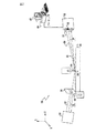
22 サンプル
24 可動ステージ
26 X線源
27 収束光線
29 反射X線
30 ディテクタ部
32 ディテクタアレイ
36 ナイフエッジ
38 シャッター
39 スリット
40 信号プロセッサ
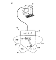
70 クラスターツール
72 蒸着ステーション
74 検査ステーション
77 ウェハ
78 ロボット
80 システムコントローラ
82 ワークステーション
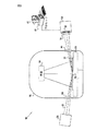
90 半導体ウェハ製造システム
92 真空チャンバー
94 蒸着装置
96 X線窓
Claims (21)
- 表面層を備えたサンプルの検査方法であって、
X線の平行光線でサンプルを照射中に、サンプルの第1の反射率スペクトルを取得し、
前記サンプルの散漫反射特性を測定するために前記第1の反射率スペクトルを処理し、
X線の収束光線で前記サンプルを照射中に、前記サンプルの第2の反射率スペクトルを取得し、
前記サンプルの表面層の特性を求めるために前記散漫反射特性を使用して前記第2の反射率スペクトルを解析することを特徴とする検査方法。 - 前記第1の反射率スペクトルの取得は、収束光線を平行にするために該光線中にスリットを導入することを含む、請求項1に記載の検査方法。
- 前記第1の反射率スペクトルの取得は、所定の入射角で平行光線で前記サンプルを照射し、且つディテクタアレイを用いて仰角の範囲にわたって同時にX線を受光することを含む、請求項1に記載の検査方法。
- 前記第2の反射率スペクトルの取得は、前記第1の反射率スペクトルの取得で使用するディテクタアレイを使用して、仰角の範囲にわたって同時にX線を受光することを含む、請求項3に記載の検査方法。
- 前記第1の反射率スペクトルの処理は、前記第1の反射率スペクトルにおいてヨネダウイングを検出することを含む、請求項1に記載の検査方法。
- 前記ヨネダウイングの検出は、前記ヨネダウイングの角度位置に応じて前記サンプルの全反射の臨界角を求めることを含む、請求項5に記載の検査方法。
- 前記ヨネダウイングの検出は、前記ヨネダウイングの振幅に応じて前記表面層のラフネスの尺度を求めることを含む、請求項5に記載の検査方法。
- 前記第2の反射率スペクトルの解析は、前記第1の反射率スペクトルに応じて散漫反射ノイズを評価し、且つ前記第2の反射率スペクトルから該散漫反射ノイズを減じることを含む、請求項1に記載の検査方法。
- 前記第2の反射率スペクトルの解析は、前記表面層の密度、厚さ、及び表面ラフネスの少なくとも一つを求めることを含む、請求項1に記載の検査方法。
- 前記サンプルは半導体ウェハであり、且つ前記第2の反射率スペクトルの解析は、該ウェハに形成された薄膜層の質を求めることを含む、請求項1に記載の検査方法。
- 表面層を備えたサンプルの検査装置であって、
前記装置の第1の構成において前記サンプルの表面へX線の平行光線を向け、且つ前記装置の第2の構成において前記サンプルの表面へX線の収束光線を向けるように適合される放射線源と、
前記第1及び第2の構成において、それぞれ前記表面に対する仰角の関数として第1及び第2の反射率スペクトルを生成するために、前記表面から反射されたX線を検知するように配置されるディテクタ部と、
前記サンプルの散漫反射特性を測定するために前記第1の反射率スペクトルを受信及び処理し、且つ前記サンプルの表面層の特性を求めるために該散漫反射特性を使用して前記第2の反射率スペクトルを解析するように結合される信号プロセッサと、
を有することを特徴とする検査装置。 - 前記第1の構成において光線を平行にするために、前記放射線源で生じた収束光線中に導入されるスリットを有する、請求項11に記載の検査装置。
- 前記ディテクタ部は、前記第1及び第2の構成の両方において、仰角の範囲にわたって同時に反射X線を受光するように構成されたディテクタアレイを有する、請求項11に記載の検査装置。
- 前記信号プロセッサは、前記第1の反射率スペクトルにおいてヨネダウイングを検出するために前記第1の反射率スペクトルを処理するように適合される、請求項11に記載の検査装置。
- 前記信号処理プロセッサは、前記ヨネダウイングの角度位置に応じて前記サンプルの全反射の臨界角を求めるように適合される、請求項14に記載の検査装置。
- 前記信号処理プロセッサは、前記ヨネダウイングの振幅に応じて前記表面層のラフネスの尺度を求めるように適合される、請求項14に記載の検査装置。
- 前記信号処理プロセッサは、前記第1の反射率スペクトルに応じて散漫反射ノイズを評価し、且つ前記第2の反射率スペクトルから該散漫反射ノイズを減じるように適合される、請求項11に記載の検査装置。
- 前記信号処理プロセッサは、前記表面層の密度、厚さ、及び表面ラフネスの少なくとも一つを求めるために前記第2の反射率スペクトルを解析するように適合される、請求項11に記載の検査装置。
- 前記サンプルは半導体ウェハであり、且つ前記信号処理プロセッサは前記ウェハに形成された薄膜層の質を求めるために前記第2の反射率スペクトルを解析するように適合される、請求項11に記載の検査装置。
- 半導体ウェハの表面に薄膜層を蒸着するように適合される蒸着ステーションと、
検査ステーションであって、
該検査ステーションの第1の構成において前記サンプルの表面へX線の平行光線を向け、且つ該検査ステーションの第2の構成において前記サンプルの表面へX線の収束光線を向けるように適合される放射線源と、
前記第1及び第2の構成において、それぞれ前記表面に対する仰角の関数として第1及び第2の反射率スペクトルを生成するために、前記表面から反射されたX線を検知するように配置されるディテクタ部と、
前記表面の散漫反射特性を測定するために前記第1の反射率スペクトルを受信及び処理し、且つ前記薄膜層の特性を求めるために該散漫反射特性を使用して前記第2の反射率スペクトルを解析するように結合される信号処理プロセッサとを有する検査ステーションと、
を有することを特徴とするマイクロ電子デバイス製造用クラスタツール。 - 半導体ウェハを受け取るように適合される製造チャンバーと、
前記チャンバー内で前記半導体ウェハの表面に薄膜層を蒸着するように適合される蒸着装置と、
放射線源であって、
該線源の第1の構成において前記製造チャンバー内の前記ウェハの表面へX線の平行光線を向け、且つ該線源の第2の構成において前記製造チャンバー内の前記ウェハの表面へX線の収束光線を向けるように適合される放射線源と、
前記第1及び第2の構成において、それぞれ前記表面に対する仰角の関数として第1及び第2の反射率スペクトルを生成するために、前記製造チャンバー内の前記表面から反射されたX線を検知するように配置されるディテクタ部と、
前記表面の散漫反射特性を測定するために前記第1の反射率スペクトルを受信及び処理し、且つ前記薄膜層の特性を求めるために該散漫反射特性を使用して前記第2の反射率スペクトルを解析するように結合される信号処理プロセッサと、
を有することを特徴とするマイクロ電子デバイスの製造装置。
Applications Claiming Priority (1)
| Application Number | Priority Date | Filing Date | Title |
|---|---|---|---|
| US10/902,177 US7068753B2 (en) | 2004-07-30 | 2004-07-30 | Enhancement of X-ray reflectometry by measurement of diffuse reflections |
Publications (2)
| Publication Number | Publication Date |
|---|---|
| JP2006058293A true JP2006058293A (ja) | 2006-03-02 |
| JP2006058293A5 JP2006058293A5 (ja) | 2008-08-14 |
Family
ID=35732192
Family Applications (1)
| Application Number | Title | Priority Date | Filing Date |
|---|---|---|---|
| JP2005221372A Pending JP2006058293A (ja) | 2004-07-30 | 2005-07-29 | サンプルの検査方法と検査装置、及びマイクロ電子デバイスの製造装置 |
Country Status (4)
| Country | Link |
|---|---|
| US (2) | US7068753B2 (ja) |
| JP (1) | JP2006058293A (ja) |
| KR (1) | KR101242520B1 (ja) |
| TW (1) | TWI411775B (ja) |
Cited By (1)
| Publication number | Priority date | Publication date | Assignee | Title |
|---|---|---|---|---|
| JP2009109387A (ja) * | 2007-10-31 | 2009-05-21 | Fujitsu Ltd | 試料分析装置および試料分析方法 |
Families Citing this family (21)
| Publication number | Priority date | Publication date | Assignee | Title |
|---|---|---|---|---|
| US7120228B2 (en) * | 2004-09-21 | 2006-10-10 | Jordan Valley Applied Radiation Ltd. | Combined X-ray reflectometer and diffractometer |
| US7804934B2 (en) | 2004-12-22 | 2010-09-28 | Jordan Valley Semiconductors Ltd. | Accurate measurement of layer dimensions using XRF |
| US7605366B2 (en) | 2005-09-21 | 2009-10-20 | Troxler Electronic Laboratories, Inc. | Nuclear density gauge |
| KR101374308B1 (ko) * | 2005-12-23 | 2014-03-14 | 조르단 밸리 세미컨덕터즈 리미티드 | Xrf를 사용한 층 치수의 정밀 측정법 |
| US20070274447A1 (en) * | 2006-05-15 | 2007-11-29 | Isaac Mazor | Automated selection of X-ray reflectometry measurement locations |
| IL180482A0 (en) * | 2007-01-01 | 2007-06-03 | Jordan Valley Semiconductors | Inspection of small features using x - ray fluorescence |
| US7920676B2 (en) * | 2007-05-04 | 2011-04-05 | Xradia, Inc. | CD-GISAXS system and method |
| US7680243B2 (en) * | 2007-09-06 | 2010-03-16 | Jordan Valley Semiconductors Ltd. | X-ray measurement of properties of nano-particles |
| US8243878B2 (en) * | 2010-01-07 | 2012-08-14 | Jordan Valley Semiconductors Ltd. | High-resolution X-ray diffraction measurement with enhanced sensitivity |
| US8687766B2 (en) | 2010-07-13 | 2014-04-01 | Jordan Valley Semiconductors Ltd. | Enhancing accuracy of fast high-resolution X-ray diffractometry |
| US8437450B2 (en) | 2010-12-02 | 2013-05-07 | Jordan Valley Semiconductors Ltd. | Fast measurement of X-ray diffraction from tilted layers |
| US8781070B2 (en) | 2011-08-11 | 2014-07-15 | Jordan Valley Semiconductors Ltd. | Detection of wafer-edge defects |
| US9390984B2 (en) | 2011-10-11 | 2016-07-12 | Bruker Jv Israel Ltd. | X-ray inspection of bumps on a semiconductor substrate |
| US9389192B2 (en) | 2013-03-24 | 2016-07-12 | Bruker Jv Israel Ltd. | Estimation of XRF intensity from an array of micro-bumps |
| US9551677B2 (en) * | 2014-01-21 | 2017-01-24 | Bruker Jv Israel Ltd. | Angle calibration for grazing-incidence X-ray fluorescence (GIXRF) |
| US9632043B2 (en) | 2014-05-13 | 2017-04-25 | Bruker Jv Israel Ltd. | Method for accurately determining the thickness and/or elemental composition of small features on thin-substrates using micro-XRF |
| US9726624B2 (en) | 2014-06-18 | 2017-08-08 | Bruker Jv Israel Ltd. | Using multiple sources/detectors for high-throughput X-ray topography measurement |
| US9829448B2 (en) | 2014-10-30 | 2017-11-28 | Bruker Jv Israel Ltd. | Measurement of small features using XRF |
| IL253578B (en) | 2017-07-19 | 2018-06-28 | Nova Measuring Instr Ltd | Measurement of patterns using x-rays |
| US11703464B2 (en) | 2018-07-28 | 2023-07-18 | Bruker Technologies Ltd. | Small-angle x-ray scatterometry |
| US11781999B2 (en) | 2021-09-05 | 2023-10-10 | Bruker Technologies Ltd. | Spot-size control in reflection-based and scatterometry-based X-ray metrology systems |
Citations (9)
| Publication number | Priority date | Publication date | Assignee | Title |
|---|---|---|---|---|
| JPH08154891A (ja) * | 1994-12-07 | 1996-06-18 | Olympus Optical Co Ltd | 内視鏡照明システム |
| JPH09184984A (ja) * | 1995-12-28 | 1997-07-15 | Ishikawajima Harima Heavy Ind Co Ltd | 顕微鏡 |
| JPH09229879A (ja) * | 1996-02-20 | 1997-09-05 | Rigaku Corp | X線装置 |
| JPH1130511A (ja) * | 1997-07-10 | 1999-02-02 | Hitachi Ltd | 表面形状検査装置 |
| JP2003004670A (ja) * | 2001-04-12 | 2003-01-08 | Jordan Valley Applied Radiation Ltd | X線反射装置 |
| JP2003202305A (ja) * | 2001-10-26 | 2003-07-18 | Rigaku Corp | 密度不均一多層膜解析方法ならびにその装置およびシステム |
| JP2004093521A (ja) * | 2002-09-04 | 2004-03-25 | Fujitsu Ltd | X線反射率測定装置および方法 |
| JP2004514135A (ja) * | 2000-11-20 | 2004-05-13 | コーニンクレッカ フィリップス エレクトロニクス エヌ ヴィ | サンプル状態検査装置及び方法 |
| JP2004245840A (ja) * | 2003-02-12 | 2004-09-02 | Jordan Valley Applied Radiation Ltd | 小角散乱測定を含むx線反射率測定 |
Family Cites Families (52)
| Publication number | Priority date | Publication date | Assignee | Title |
|---|---|---|---|---|
| US3980568A (en) | 1975-10-17 | 1976-09-14 | Hankison Corporation | Radiation detection system |
| US4525853A (en) | 1983-10-17 | 1985-06-25 | Energy Conversion Devices, Inc. | Point source X-ray focusing device |
| US4725963A (en) | 1985-05-09 | 1988-02-16 | Scientific Measurement Systems I, Ltd. | Method and apparatus for dimensional analysis and flaw detection of continuously produced tubular objects |
| US4715718A (en) * | 1985-06-24 | 1987-12-29 | The Dow Chemical Company | Method and apparatus for on-line monitoring of laminate bond strength |
| DE3606748C1 (de) * | 1986-03-01 | 1987-10-01 | Geesthacht Gkss Forschung | Anordnung zur zerstoerungsfreien Messung von Metallspuren |
| US4989226A (en) | 1987-08-21 | 1991-01-29 | Brigham Young University | Layered devices having surface curvature |
| JPS6448398U (ja) | 1987-09-21 | 1989-03-24 | ||
| JP2742415B2 (ja) | 1987-11-27 | 1998-04-22 | 株式会社日立製作所 | X線分析装置 |
| NL8801019A (nl) | 1988-04-20 | 1989-11-16 | Philips Nv | Roentgen spectrometer met dubbel gebogen kristal. |
| JP2890553B2 (ja) | 1989-11-24 | 1999-05-17 | 株式会社島津製作所 | X線像撮像装置 |
| JPH05188019A (ja) | 1991-07-23 | 1993-07-27 | Hitachi Ltd | X線複合分析装置 |
| JPH05291152A (ja) * | 1992-04-15 | 1993-11-05 | Hitachi Ltd | X線分析装置及びこれを用いた半導体製造装置 |
| JP2720131B2 (ja) | 1992-05-15 | 1998-02-25 | 株式会社日立製作所 | X線反射プロファイル測定方法及び装置 |
| US5493122A (en) | 1994-02-04 | 1996-02-20 | Nucleonics Development Company | Energy resolving x-ray detector |
| JP3109789B2 (ja) | 1994-05-18 | 2000-11-20 | 理学電機株式会社 | X線反射率測定方法 |
| US5570408A (en) | 1995-02-28 | 1996-10-29 | X-Ray Optical Systems, Inc. | High intensity, small diameter x-ray beam, capillary optic system |
| US5619548A (en) | 1995-08-11 | 1997-04-08 | Oryx Instruments And Materials Corp. | X-ray thickness gauge |
| US5740226A (en) | 1995-11-30 | 1998-04-14 | Fujitsu Limited | Film thickness measuring and film forming method |
| US5744950A (en) * | 1996-05-09 | 1998-04-28 | Ssi Technologies, Inc. | Apparatus for detecting the speed of a rotating element including signal conditioning to provide a fifty percent duty cycle |
| JP3674149B2 (ja) | 1996-05-22 | 2005-07-20 | 井関農機株式会社 | 野菜収穫機 |
| JPH09329557A (ja) | 1996-06-11 | 1997-12-22 | Seiko Instr Inc | マイクロ蛍光x線分析装置 |
| US5798525A (en) | 1996-06-26 | 1998-08-25 | International Business Machines Corporation | X-ray enhanced SEM critical dimension measurement |
| JP2984232B2 (ja) | 1996-10-25 | 1999-11-29 | 株式会社テクノス研究所 | X線分析装置およびx線照射角設定方法 |
| US6041098A (en) | 1997-02-03 | 2000-03-21 | Touryanski; Alexander G. | X-ray reflectometer |
| JPH1114561A (ja) | 1997-04-30 | 1999-01-22 | Rigaku Corp | X線測定装置およびその方法 |
| DE19744986C1 (de) * | 1997-10-13 | 1999-02-11 | Karl Hehl | Formschließeinheit für eine Spritzgießmaschine |
| US6628740B2 (en) | 1997-10-17 | 2003-09-30 | The Regents Of The University Of California | Controlled fusion in a field reversed configuration and direct energy conversion |
| US5963329A (en) | 1997-10-31 | 1999-10-05 | International Business Machines Corporation | Method and apparatus for measuring the profile of small repeating lines |
| US6005915A (en) | 1997-11-07 | 1999-12-21 | Advanced Micro Devices, Inc. | Apparatus and method for measuring the roughness of a target material surface based upon the scattering of incident X-ray photons |
| DE19820861B4 (de) | 1998-05-09 | 2004-09-16 | Bruker Axs Gmbh | Simultanes Röntgenfluoreszenz-Spektrometer |
| DE19833524B4 (de) | 1998-07-25 | 2004-09-23 | Bruker Axs Gmbh | Röntgen-Analysegerät mit Gradienten-Vielfachschicht-Spiegel |
| US6094256A (en) | 1998-09-29 | 2000-07-25 | Nikon Precision Inc. | Method for forming a critical dimension test structure and its use |
| US6192103B1 (en) | 1999-06-03 | 2001-02-20 | Bede Scientific, Inc. | Fitting of X-ray scattering data using evolutionary algorithms |
| US6389102B2 (en) | 1999-09-29 | 2002-05-14 | Jordan Valley Applied Radiation Ltd. | X-ray array detector |
| US6381303B1 (en) | 1999-09-29 | 2002-04-30 | Jordan Valley Applied Radiation Ltd. | X-ray microanalyzer for thin films |
| NL1016871C1 (nl) | 1999-12-24 | 2001-06-26 | Koninkl Philips Electronics Nv | Toestel voor r÷ntgenanalyse met een CCD-device als r÷ntgendetector. |
| US6453006B1 (en) | 2000-03-16 | 2002-09-17 | Therma-Wave, Inc. | Calibration and alignment of X-ray reflectometric systems |
| JP2001349849A (ja) | 2000-04-04 | 2001-12-21 | Rigaku Corp | 密度不均一試料解析方法ならびにその装置およびシステム |
| US6504902B2 (en) | 2000-04-10 | 2003-01-07 | Rigaku Corporation | X-ray optical device and multilayer mirror for small angle scattering system |
| US6970532B2 (en) | 2000-05-10 | 2005-11-29 | Rigaku Corporation | Method and apparatus for measuring thin film, and thin film deposition system |
| JP3483136B2 (ja) * | 2000-07-10 | 2004-01-06 | 株式会社島津製作所 | X線回折装置 |
| US6556652B1 (en) | 2000-08-09 | 2003-04-29 | Jordan Valley Applied Radiation Ltd. | Measurement of critical dimensions using X-rays |
| US6744850B2 (en) | 2001-01-11 | 2004-06-01 | Therma-Wave, Inc. | X-ray reflectance measurement system with adjustable resolution |
| US6744950B2 (en) | 2001-01-18 | 2004-06-01 | Veridian Systems | Correlators and cross-correlators using tapped optical fibers |
| US6611576B1 (en) * | 2001-02-12 | 2003-08-26 | Advanced Micro Devices, Inc. | Automated control of metal thickness during film deposition |
| US6512814B2 (en) | 2001-04-12 | 2003-01-28 | Jordan Valley Applied Radiation | X-ray reflectometer |
| US6507634B1 (en) | 2001-09-19 | 2003-01-14 | Therma-Wave, Inc. | System and method for X-ray reflectometry measurement of low density films |
| US6771735B2 (en) | 2001-11-07 | 2004-08-03 | Kla-Tencor Technologies Corporation | Method and apparatus for improved x-ray reflection measurement |
| US6810105B2 (en) | 2002-01-25 | 2004-10-26 | Kla-Tencor Technologies Corporation | Methods and apparatus for dishing and erosion characterization |
| US6680996B2 (en) | 2002-02-19 | 2004-01-20 | Jordan Valley Applied Radiation Ltd. | Dual-wavelength X-ray reflectometry |
| US6711232B1 (en) | 2003-04-16 | 2004-03-23 | Kla-Tencor Technologies Corporation | X-ray reflectivity measurement |
| US7120228B2 (en) * | 2004-09-21 | 2006-10-10 | Jordan Valley Applied Radiation Ltd. | Combined X-ray reflectometer and diffractometer |
-
2004
- 2004-07-30 US US10/902,177 patent/US7068753B2/en active Active
-
2005
- 2005-07-29 TW TW094125805A patent/TWI411775B/zh active
- 2005-07-29 JP JP2005221372A patent/JP2006058293A/ja active Pending
- 2005-07-29 KR KR1020050069238A patent/KR101242520B1/ko active IP Right Grant
-
2006
- 2006-04-04 US US11/396,719 patent/US7231016B2/en active Active
Patent Citations (9)
| Publication number | Priority date | Publication date | Assignee | Title |
|---|---|---|---|---|
| JPH08154891A (ja) * | 1994-12-07 | 1996-06-18 | Olympus Optical Co Ltd | 内視鏡照明システム |
| JPH09184984A (ja) * | 1995-12-28 | 1997-07-15 | Ishikawajima Harima Heavy Ind Co Ltd | 顕微鏡 |
| JPH09229879A (ja) * | 1996-02-20 | 1997-09-05 | Rigaku Corp | X線装置 |
| JPH1130511A (ja) * | 1997-07-10 | 1999-02-02 | Hitachi Ltd | 表面形状検査装置 |
| JP2004514135A (ja) * | 2000-11-20 | 2004-05-13 | コーニンクレッカ フィリップス エレクトロニクス エヌ ヴィ | サンプル状態検査装置及び方法 |
| JP2003004670A (ja) * | 2001-04-12 | 2003-01-08 | Jordan Valley Applied Radiation Ltd | X線反射装置 |
| JP2003202305A (ja) * | 2001-10-26 | 2003-07-18 | Rigaku Corp | 密度不均一多層膜解析方法ならびにその装置およびシステム |
| JP2004093521A (ja) * | 2002-09-04 | 2004-03-25 | Fujitsu Ltd | X線反射率測定装置および方法 |
| JP2004245840A (ja) * | 2003-02-12 | 2004-09-02 | Jordan Valley Applied Radiation Ltd | 小角散乱測定を含むx線反射率測定 |
Cited By (1)
| Publication number | Priority date | Publication date | Assignee | Title |
|---|---|---|---|---|
| JP2009109387A (ja) * | 2007-10-31 | 2009-05-21 | Fujitsu Ltd | 試料分析装置および試料分析方法 |
Also Published As
| Publication number | Publication date |
|---|---|
| TW200619612A (en) | 2006-06-16 |
| US7068753B2 (en) | 2006-06-27 |
| US20060182220A1 (en) | 2006-08-17 |
| US20060023836A1 (en) | 2006-02-02 |
| KR101242520B1 (ko) | 2013-03-12 |
| US7231016B2 (en) | 2007-06-12 |
| KR20060048904A (ko) | 2006-05-18 |
| TWI411775B (zh) | 2013-10-11 |
Similar Documents
| Publication | Publication Date | Title |
|---|---|---|
| JP2006058293A (ja) | サンプルの検査方法と検査装置、及びマイクロ電子デバイスの製造装置 | |
| US7130376B2 (en) | X-ray reflectometry of thin film layers with enhanced accuracy | |
| TWI395943B (zh) | 用於分析具有一表面層之一樣品之裝置及方法,及用於生產微電子器件之叢集工具及裝置 | |
| US6895075B2 (en) | X-ray reflectometry with small-angle scattering measurement | |
| JP5980822B2 (ja) | 表面検査を行う方法 | |
| JP4519455B2 (ja) | X線反射計用のビームセンタリング方法及び角度較正方法 | |
| TWI518315B (zh) | 用於x射線分析之方法及裝置 | |
| KR101040555B1 (ko) | 반사 모드에서 x-레이 회절을 사용하여 크리티컬 디멘션을측정하는 방법 및 장치 | |
| JP5398117B2 (ja) | Xrfを用いた層寸法の正確な測定 | |
| JP2006058293A5 (ja) | ||
| US7804934B2 (en) | Accurate measurement of layer dimensions using XRF | |
| US20090074141A1 (en) | Automated selection of x-ray reflectometry measurement locations | |
| JP2007285923A (ja) | 反射モードのx線回折を用いた限界寸法の測定 | |
| KR20160051644A (ko) | Xrf를 사용한 작은 특징부의 측정 | |
| JP5302281B2 (ja) | サンプルの検査方法及び装置 | |
| JP2005140777A (ja) | サンプル検査方法、その装置、マイクロエレクトロニクス装置製造用クラスタツール、マイクロエレクトロニクス装置製造用装置 | |
| JP2001116896A (ja) | X線反射率測定方法およびその装置 |
Legal Events
| Date | Code | Title | Description |
|---|---|---|---|
| A521 | Request for written amendment filed |
Free format text: JAPANESE INTERMEDIATE CODE: A523 Effective date: 20080701 |
|
| A621 | Written request for application examination |
Free format text: JAPANESE INTERMEDIATE CODE: A621 Effective date: 20080701 |
|
| A131 | Notification of reasons for refusal |
Free format text: JAPANESE INTERMEDIATE CODE: A131 Effective date: 20100803 |
|
| A601 | Written request for extension of time |
Free format text: JAPANESE INTERMEDIATE CODE: A601 Effective date: 20101028 |
|
| A602 | Written permission of extension of time |
Free format text: JAPANESE INTERMEDIATE CODE: A602 Effective date: 20101102 |
|
| A521 | Request for written amendment filed |
Free format text: JAPANESE INTERMEDIATE CODE: A523 Effective date: 20110124 |
|
| A02 | Decision of refusal |
Free format text: JAPANESE INTERMEDIATE CODE: A02 Effective date: 20110510 |