JP2005513575A - 誘導層に薄膜アンテナ列を格子状に内蔵したタッチ制御型ディスプレイ - Google Patents
誘導層に薄膜アンテナ列を格子状に内蔵したタッチ制御型ディスプレイ Download PDFInfo
- Publication number
- JP2005513575A JP2005513575A JP2003556879A JP2003556879A JP2005513575A JP 2005513575 A JP2005513575 A JP 2005513575A JP 2003556879 A JP2003556879 A JP 2003556879A JP 2003556879 A JP2003556879 A JP 2003556879A JP 2005513575 A JP2005513575 A JP 2005513575A
- Authority
- JP
- Japan
- Prior art keywords
- induction
- induction layer
- thin film
- layer
- touch
- Prior art date
- Legal status (The legal status is an assumption and is not a legal conclusion. Google has not performed a legal analysis and makes no representation as to the accuracy of the status listed.)
- Pending
Links
Images


Classifications
-
- G—PHYSICS
- G06—COMPUTING; CALCULATING OR COUNTING
- G06F—ELECTRIC DIGITAL DATA PROCESSING
- G06F3/00—Input arrangements for transferring data to be processed into a form capable of being handled by the computer; Output arrangements for transferring data from processing unit to output unit, e.g. interface arrangements
- G06F3/01—Input arrangements or combined input and output arrangements for interaction between user and computer
- G06F3/03—Arrangements for converting the position or the displacement of a member into a coded form
- G06F3/041—Digitisers, e.g. for touch screens or touch pads, characterised by the transducing means
- G06F3/046—Digitisers, e.g. for touch screens or touch pads, characterised by the transducing means by electromagnetic means
-
- G—PHYSICS
- G06—COMPUTING; CALCULATING OR COUNTING
- G06F—ELECTRIC DIGITAL DATA PROCESSING
- G06F3/00—Input arrangements for transferring data to be processed into a form capable of being handled by the computer; Output arrangements for transferring data from processing unit to output unit, e.g. interface arrangements
- G06F3/01—Input arrangements or combined input and output arrangements for interaction between user and computer
- G06F3/03—Arrangements for converting the position or the displacement of a member into a coded form
- G06F3/041—Digitisers, e.g. for touch screens or touch pads, characterised by the transducing means
- G06F3/0416—Control or interface arrangements specially adapted for digitisers
Abstract
【解決手段】 誘導層に薄膜アンテナ列を格子状に内蔵したタッチ制御型ディスプレイとして、少なくともタッチ制御型ディスプレイスクリーンと本体とを有し、誘導層はタッチ制御型ディスプレイスクリーンの後方に配置され、この誘導層の出力端は誘導制御回路に接続し、本体内にはタッチ型ディスプレイ制御回路が配置されている。誘導層は絶縁薄膜上にX、Y軸方向に沿って形成されたアンテナ列であり、このアンテナ列の格子に包囲された単位領域が単位誘導セルを構成している。誘導層はディスプレイスクリーンの後方に配置されているので、柔軟な薄膜の表面に印刷した誘導型のアンテナ列を識別誘導部品として使用することが出来るので、製造工程が簡単となり、さらに、比較的コストを低く押さえることが出来る。その上、ディスプレイスクリーンの面積が大きくなるほど、現在の技術に対するコストが著しく軽減出来る。且つ、識別精度が高く、電磁ペン又は手による接触で、マウス情報又は筆跡情報を入力することができる。さらに、ディスプレイスクリーンの表面には防護膜が塗布されているので、物理的な損傷を容易に排除することが出来、寿命が長く、耐久性のあるディスプレイスクリーンが得られる。
【効果】 製造工程が簡単であり、コストが低く、精度が高く、且つ寿命が長い。
Description
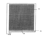
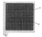
前記誘導層は、前記タッチ制御型ディスプレイスクリーンの後方に配置され、この誘導層の出力端は誘導制御回路に接続し、前記本体内には、タッチ型ディスプレイ制御回路が配置されてなる誘導層に薄膜アンテナ列を格子状に内蔵したタッチ制御型ディスプレイにおいて、誘導層は絶縁薄膜上にX、Y軸方向に沿って形成されたアンテナ列であり、このアンテナ列の格子に包囲された単位領域が、単位誘導セルを構成するものである。
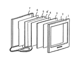
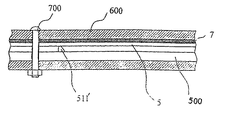
図1において、本発明は誘導層に薄膜アンテナ列を格子状に内蔵したタッチ制御型ディスプレイであり、少なくともディスプレイスクリーン3と本体1、7とを有しており、誘導層4は、ディスプレイスクリーン3の後方に配置されている。この誘導層4の出力端は、誘導制御回路に接続し、ディスプレイスクリーン制御回路6は、本体1、7内に配置されている。ディスプレイスクリーン3は、プラズマディスプレイあるいはタッチ式の液晶フラット型ディスプレイである。
2 保護膜
3 ディスプレイスクリーン
4、4’ 誘導層
5 被覆層
6 ディスプレイ制御回路
7 バッファー層
8、500 印刷線路基板
51、52 アンテナ列
53 単位誘導セル
55 絶縁薄膜
Claims (22)
- 誘導層に薄膜アンテナ列を格子状に内蔵したタッチ制御型ディスプレイとして、少なくともタッチ制御型ディスプレイスクリーンと本体とを有し、
前記誘導層は、前記タッチ制御型ディスプレイスクリーンの後方に配置され、この誘導層の出力端は誘導制御回路に接続し、前記本体内には、タッチ型ディスプレイ制御回路が配置されてなる誘導層に薄膜アンテナ列を格子状に内蔵したタッチ制御型ディスプレイにおいて、
前記誘導層は絶縁薄膜上にX、Y軸方向に沿って形成されたアンテナ列であり、
このアンテナ列の格子に包囲された単位領域が、単位誘導セルを構成すること
を特徴とする誘導層に薄膜アンテナ列を格子状に内蔵したタッチ制御型ディスプレイ。 - 前記誘導層の面積と前記ディスプレイスクリーンの面積と同じであるかあるいはこのディスプレイスクリーンの面積より小さいこと
を特徴とする請求項1に記載の誘導層に薄膜アンテナ列を格子状に内蔵したタッチ制御型ディスプレイ。 - 前記誘導層の面積は、前記ディスプレイスクリーンの面積より小さくするとともに、前記誘導層は、前記ディスプレイスクリーンの表示範囲の片方あるいは中央部に配置したこと
を特徴とする請求項2に記載の誘導層に薄膜アンテナ列を格子状に内蔵したタッチ制御型ディスプレイ。 - 前記誘導層の後方に、装置の耐干渉能力を強化するための被覆層を配置したこと
を特徴とする請求項1に記載の誘導層に薄膜アンテナ列を格子状に内蔵したタッチ制御型ディスプレイ。 - 前記誘導層と被覆層との間に、バッファー層を配置したこと
を特徴とする請求項4に記載の誘導層に薄膜アンテナ列を格子状に内蔵したタッチ制御型ディスプレイ。 - 前記被覆層とタッチ型ディスプレイ制御回路との間に、空間があること
を特徴とする請求項4あるいは請求項5に記載の誘導層に薄膜アンテナ列を格子状に内蔵したタッチ制御型ディスプレイ。 - 前記誘導層は、絶縁薄膜上を覆っている銅箔をエッチングして形成したアンテナ列であること
を特徴とする請求項1〜請求項5にそれぞれ記載の誘導層に薄膜アンテナ列を格子状に内蔵したタッチ制御型ディスプレイ。 - 前記誘導層は、可撓性印刷回路(FPC)のアンテナ列であること
を特徴とする請求項7に記載の誘導層に薄膜アンテナ列を格子状に内蔵したタッチ制御型ディスプレイ。 - 前記誘導層は、絶縁薄膜上に形成した銀ペースト又は銀ペーストとカーボンペーストとの混合物により形成したアンテナであること
を特徴とする請求項1〜請求項5にそれぞれ記載の誘導層に薄膜アンテナ列を格子状に内蔵したタッチ制御型ディスプレイ。 - 前記誘導層は、前記絶縁薄膜の両面あるいは片面に形成することにより、一方の絶縁薄膜の上に他方の絶縁薄膜を重ねた重複構造としたこと
を特徴とする請求項9に記載の誘導層に薄膜アンテナ列を格子状に内蔵したタッチ制御型ディスプレイ。 - 前記絶縁薄膜は、フィルム状材質であること
を特徴とする請求項9に記載の誘導層に薄膜アンテナ列を格子状に内蔵したタッチ制御型ディスプレイ。 - 前記誘導層は少なくとも1枚以上であり、
各誘導層上の各単位誘導セルは、交互に交差分布していること
を特徴とする請求項1〜請求項5にそれぞれ記載の誘導層に薄膜アンテナ列を格子状に内蔵したタッチ制御型ディスプレイ。 - 前記各誘導層上の各単位誘導セルの単位領域の大きさは、いずれも同一あるいは異なる大きさであること
を特徴とする請求項12に記載の誘導層に薄膜アンテナ列を格子状に内蔵したタッチ制御型ディスプレイ。 - 前記誘導層と前記誘導制御回路とは一体化して直接接続され、
この誘導制御回路の機器は、前記アンテナ列の出力端子に配置され、前記誘導制御回路は前記本体内に配置したこと
を特徴とする請求項1〜請求項5にそれぞれ記載の誘導層に薄膜アンテナ列を格子状に内蔵したタッチ制御型ディスプレイ。 - 前記誘導制御回路の機器は、前記誘導層から分離された印刷線路基板上に配置し、
前記誘導層の前記アンテナ列の出力端子は、圧着接続、プラグイン接続、溶接接続のいずれかの手段で、前記印刷線路基板のそれぞれ対応する入力端と接続したこと
を特徴とする請求項1〜請求項5にそれぞれ記載の誘導層に薄膜アンテナ列を格子状に内蔵したタッチ制御型ディスプレイ。 - 前記誘導層の前記アンテナ列の出力端子は、ハードシートと印刷線路基板との間に配置し、
前記バッファー層は、前記ハードシートと前記アンテナ列の出力端子との間に配置し、
前記ハードシートと前記バッファー層と前記アンテナ列の出力端子とは、ひねられた状態で印刷線路基板に重ねた重複構造とし、
前記アンテナ列の出力端子は、印刷線路基板の対応する入力端子に接続したこと
を特徴とする請求項15に記載の誘導層に薄膜アンテナ列を格子状に内蔵したタッチ制御型ディスプレイ。 - 前記印刷線路基板は、タッチ型ディスプレイスクリーンの前記本体内のディスプレイスクリーン制御回路の印刷線路基板であること
を特徴とする請求項15に記載の誘導層に薄膜アンテナ列を格子状に内蔵したタッチ制御型ディスプレイ。 - 前記印刷線路基板は、タッチ型ディスプレイスクリーンの本体外のディスプレイスクリーン制御回路の印刷線路基板であり、あるいは独立ユニットであり、あるいはPCのメインボードに配置したものであり、
これら相互の接続は、線路あるいはケーブル接続であること
を特徴とする請求項15に記載の誘導層に薄膜アンテナ列を格子状に内蔵したタッチ制御型ディスプレイ。 - 前記誘導制御回路は、前記本体外に配置し、
この本体とは電気的な接続手段を介して接続し、
前記誘導層の前記アンテナ列の出力端子は、圧着接続、プラグイン接続、溶接接続のいずれかの手段で、前記誘導層の出力インタフェースを介して接続し、
前記誘導層の電気的な接続手段と整合させるためのインタフェースは、制御回路により提供されること
を特徴とする請求項18に記載の誘導層に薄膜アンテナ列を格子状に内蔵したタッチ制御型ディスプレイ。 - 前記誘導層の出力インタフェースと制御回路のインタフェースとは、ピン型接続、可撓性印刷回路(FPC)、ピン−ピン接続、溶接スポット(VGA)熱溶接接続、超音波溶接、半田プレート溶接装置、破壊型接続のいずれかで接続すること
を特徴とする請求項19に記載の誘導層に薄膜アンテナ列を格子状に内蔵したタッチ制御型ディスプレイ。 - 前記ディスプレイスクリーンの前面に、保護層を配置したこと
を特徴とする請求項1〜請求項5にそれぞれ記載の誘導層に薄膜アンテナ列を格子状に内蔵したタッチ制御型ディスプレイ。 - 前記プラズマディスプレイスクリーンあるいは液晶ディスプレイスクリーンであること
を特徴とする請求項1〜請求項5にそれぞれ記載の誘導層に薄膜アンテナ列を格子状に内蔵したタッチ制御型ディスプレイ。
Applications Claiming Priority (3)
| Application Number | Priority Date | Filing Date | Title |
|---|---|---|---|
| CN01279677.8U CN2512043Y (zh) | 2001-12-29 | 2001-12-29 | 具有柔性隔膜式电磁感应发生装置的电子白板 |
| CN 02257335 CN2569259Y (zh) | 2002-09-16 | 2002-09-16 | 内置隔膜天线阵列网格电磁感应层的触摸控制显示屏 |
| PCT/CN2002/000687 WO2003056422A1 (en) | 2001-12-29 | 2002-09-27 | A touch control display screen with a built-in electromagnet induction layer of septum array grids |
Publications (2)
| Publication Number | Publication Date |
|---|---|
| JP2005513575A true JP2005513575A (ja) | 2005-05-12 |
| JP2005513575A5 JP2005513575A5 (ja) | 2005-12-22 |
Family
ID=25741085
Family Applications (1)
| Application Number | Title | Priority Date | Filing Date |
|---|---|---|---|
| JP2003556879A Pending JP2005513575A (ja) | 2001-12-29 | 2002-09-27 | 誘導層に薄膜アンテナ列を格子状に内蔵したタッチ制御型ディスプレイ |
Country Status (6)
| Country | Link |
|---|---|
| US (1) | US7796122B2 (ja) |
| EP (1) | EP1469383A4 (ja) |
| JP (1) | JP2005513575A (ja) |
| KR (1) | KR100605901B1 (ja) |
| AU (1) | AU2002338134A1 (ja) |
| WO (1) | WO2003056422A1 (ja) |
Families Citing this family (148)
| Publication number | Priority date | Publication date | Assignee | Title |
|---|---|---|---|---|
| CN2512043Y (zh) * | 2001-12-29 | 2002-09-18 | 台均实业有限公司 | 具有柔性隔膜式电磁感应发生装置的电子白板 |
| US8416174B2 (en) * | 2003-12-08 | 2013-04-09 | Canon Kabushiki Kaisha | Display apparatus |
| US7450109B2 (en) * | 2004-07-13 | 2008-11-11 | International Business Machines Corporation | Electronic whiteboard |
| US7436394B2 (en) * | 2004-07-13 | 2008-10-14 | International Business Machines Corporation | Apparatus, system and method of importing data arranged in a table on an electronic whiteboard into a spreadsheet |
| TWI261276B (en) * | 2005-05-13 | 2006-09-01 | Tatung Co | Touch-control acrylic-board manufacturing method |
| KR100948050B1 (ko) * | 2006-11-23 | 2010-03-19 | 주식회사 메디슨 | 휴대용 초음파 시스템 |
| US8456851B2 (en) * | 2008-05-16 | 2013-06-04 | Apple Inc. | Flex circuit with single sided routing and double sided attach |
| US8400419B2 (en) * | 2009-04-20 | 2013-03-19 | Broadcom Corporation | Dual mode inductive touch screen for use in a configurable communication device and methods for use therewith |
| US8810523B2 (en) * | 2009-04-20 | 2014-08-19 | Broadcom Corporation | Inductive touch screen and methods for use therewith |
| US8339372B2 (en) * | 2009-04-20 | 2012-12-25 | Broadcom Corporation | Inductive touch screen with integrated antenna for use in a communication device and methods for use therewith |
| US20110102331A1 (en) * | 2009-10-29 | 2011-05-05 | Qrg Limited | Redundant touchscreen electrodes |
| CN102053408B (zh) * | 2009-11-05 | 2013-04-10 | 太瀚科技股份有限公司 | 具有电磁感应回路的复合基板与显示器 |
| US20110163964A1 (en) * | 2010-01-07 | 2011-07-07 | Yen-Lung Tsai & Tsung-Chieh CHO | Dual type touch display device |
| DE102010014796A1 (de) * | 2010-02-03 | 2011-08-04 | Emerging Display Technologies Corp. | Bilschirmeinheit mit einem Tastschirm |
| US20120034888A1 (en) * | 2010-08-05 | 2012-02-09 | Franco De Flaviis | Method and System for Utilizing a Touchscreen Interface as an Antenna |
| US9184502B2 (en) | 2010-12-22 | 2015-11-10 | Intel Corporation | Antenna integrated into a touch sensor of a touchscreen display |
| US20130241854A1 (en) * | 2012-03-06 | 2013-09-19 | Industry-University Cooperation Foundation Hanyang University | Image sharing system and user terminal for the system |
| US8918565B2 (en) * | 2012-05-19 | 2014-12-23 | Robert Dennis Kennedy | Tablet computer screen and mobile phone screen to digital I/O converter |
| US9999038B2 (en) | 2013-05-31 | 2018-06-12 | At&T Intellectual Property I, L.P. | Remote distributed antenna system |
| US9525524B2 (en) | 2013-05-31 | 2016-12-20 | At&T Intellectual Property I, L.P. | Remote distributed antenna system |
| CN104571772A (zh) * | 2013-10-12 | 2015-04-29 | 上海和辉光电有限公司 | 电磁触控屏结构 |
| US8897697B1 (en) | 2013-11-06 | 2014-11-25 | At&T Intellectual Property I, Lp | Millimeter-wave surface-wave communications |
| US9768833B2 (en) | 2014-09-15 | 2017-09-19 | At&T Intellectual Property I, L.P. | Method and apparatus for sensing a condition in a transmission medium of electromagnetic waves |
| US10063280B2 (en) | 2014-09-17 | 2018-08-28 | At&T Intellectual Property I, L.P. | Monitoring and mitigating conditions in a communication network |
| US9615269B2 (en) | 2014-10-02 | 2017-04-04 | At&T Intellectual Property I, L.P. | Method and apparatus that provides fault tolerance in a communication network |
| US9685992B2 (en) | 2014-10-03 | 2017-06-20 | At&T Intellectual Property I, L.P. | Circuit panel network and methods thereof |
| US9503189B2 (en) | 2014-10-10 | 2016-11-22 | At&T Intellectual Property I, L.P. | Method and apparatus for arranging communication sessions in a communication system |
| US9973299B2 (en) | 2014-10-14 | 2018-05-15 | At&T Intellectual Property I, L.P. | Method and apparatus for adjusting a mode of communication in a communication network |
| US9577306B2 (en) | 2014-10-21 | 2017-02-21 | At&T Intellectual Property I, L.P. | Guided-wave transmission device and methods for use therewith |
| US9769020B2 (en) | 2014-10-21 | 2017-09-19 | At&T Intellectual Property I, L.P. | Method and apparatus for responding to events affecting communications in a communication network |
| US9780834B2 (en) | 2014-10-21 | 2017-10-03 | At&T Intellectual Property I, L.P. | Method and apparatus for transmitting electromagnetic waves |
| US9312919B1 (en) | 2014-10-21 | 2016-04-12 | At&T Intellectual Property I, Lp | Transmission device with impairment compensation and methods for use therewith |
| US9653770B2 (en) | 2014-10-21 | 2017-05-16 | At&T Intellectual Property I, L.P. | Guided wave coupler, coupling module and methods for use therewith |
| US9627768B2 (en) | 2014-10-21 | 2017-04-18 | At&T Intellectual Property I, L.P. | Guided-wave transmission device with non-fundamental mode propagation and methods for use therewith |
| KR102175750B1 (ko) | 2014-10-29 | 2020-11-06 | 삼성전자주식회사 | 안테나 장치 및 이를 구비하는 전자 장치 |
| US9544006B2 (en) | 2014-11-20 | 2017-01-10 | At&T Intellectual Property I, L.P. | Transmission device with mode division multiplexing and methods for use therewith |
| US9742462B2 (en) | 2014-12-04 | 2017-08-22 | At&T Intellectual Property I, L.P. | Transmission medium and communication interfaces and methods for use therewith |
| US9997819B2 (en) | 2015-06-09 | 2018-06-12 | At&T Intellectual Property I, L.P. | Transmission medium and method for facilitating propagation of electromagnetic waves via a core |
| US10340573B2 (en) | 2016-10-26 | 2019-07-02 | At&T Intellectual Property I, L.P. | Launcher with cylindrical coupling device and methods for use therewith |
| US9800327B2 (en) | 2014-11-20 | 2017-10-24 | At&T Intellectual Property I, L.P. | Apparatus for controlling operations of a communication device and methods thereof |
| US9954287B2 (en) | 2014-11-20 | 2018-04-24 | At&T Intellectual Property I, L.P. | Apparatus for converting wireless signals and electromagnetic waves and methods thereof |
| US10243784B2 (en) | 2014-11-20 | 2019-03-26 | At&T Intellectual Property I, L.P. | System for generating topology information and methods thereof |
| US9461706B1 (en) | 2015-07-31 | 2016-10-04 | At&T Intellectual Property I, Lp | Method and apparatus for exchanging communication signals |
| US10009067B2 (en) | 2014-12-04 | 2018-06-26 | At&T Intellectual Property I, L.P. | Method and apparatus for configuring a communication interface |
| US9876570B2 (en) | 2015-02-20 | 2018-01-23 | At&T Intellectual Property I, Lp | Guided-wave transmission device with non-fundamental mode propagation and methods for use therewith |
| US9749013B2 (en) | 2015-03-17 | 2017-08-29 | At&T Intellectual Property I, L.P. | Method and apparatus for reducing attenuation of electromagnetic waves guided by a transmission medium |
| US9705561B2 (en) | 2015-04-24 | 2017-07-11 | At&T Intellectual Property I, L.P. | Directional coupling device and methods for use therewith |
| US10224981B2 (en) | 2015-04-24 | 2019-03-05 | At&T Intellectual Property I, Lp | Passive electrical coupling device and methods for use therewith |
| US9793954B2 (en) | 2015-04-28 | 2017-10-17 | At&T Intellectual Property I, L.P. | Magnetic coupling device and methods for use therewith |
| US9748626B2 (en) | 2015-05-14 | 2017-08-29 | At&T Intellectual Property I, L.P. | Plurality of cables having different cross-sectional shapes which are bundled together to form a transmission medium |
| US9490869B1 (en) | 2015-05-14 | 2016-11-08 | At&T Intellectual Property I, L.P. | Transmission medium having multiple cores and methods for use therewith |
| US9871282B2 (en) | 2015-05-14 | 2018-01-16 | At&T Intellectual Property I, L.P. | At least one transmission medium having a dielectric surface that is covered at least in part by a second dielectric |
| US10650940B2 (en) | 2015-05-15 | 2020-05-12 | At&T Intellectual Property I, L.P. | Transmission medium having a conductive material and methods for use therewith |
| US9917341B2 (en) | 2015-05-27 | 2018-03-13 | At&T Intellectual Property I, L.P. | Apparatus and method for launching electromagnetic waves and for modifying radial dimensions of the propagating electromagnetic waves |
| US10812174B2 (en) | 2015-06-03 | 2020-10-20 | At&T Intellectual Property I, L.P. | Client node device and methods for use therewith |
| US9866309B2 (en) | 2015-06-03 | 2018-01-09 | At&T Intellectual Property I, Lp | Host node device and methods for use therewith |
| US9912381B2 (en) | 2015-06-03 | 2018-03-06 | At&T Intellectual Property I, Lp | Network termination and methods for use therewith |
| US9913139B2 (en) | 2015-06-09 | 2018-03-06 | At&T Intellectual Property I, L.P. | Signal fingerprinting for authentication of communicating devices |
| US9820146B2 (en) | 2015-06-12 | 2017-11-14 | At&T Intellectual Property I, L.P. | Method and apparatus for authentication and identity management of communicating devices |
| US9667317B2 (en) | 2015-06-15 | 2017-05-30 | At&T Intellectual Property I, L.P. | Method and apparatus for providing security using network traffic adjustments |
| US9509415B1 (en) | 2015-06-25 | 2016-11-29 | At&T Intellectual Property I, L.P. | Methods and apparatus for inducing a fundamental wave mode on a transmission medium |
| US9865911B2 (en) | 2015-06-25 | 2018-01-09 | At&T Intellectual Property I, L.P. | Waveguide system for slot radiating first electromagnetic waves that are combined into a non-fundamental wave mode second electromagnetic wave on a transmission medium |
| US9640850B2 (en) | 2015-06-25 | 2017-05-02 | At&T Intellectual Property I, L.P. | Methods and apparatus for inducing a non-fundamental wave mode on a transmission medium |
| US10320586B2 (en) | 2015-07-14 | 2019-06-11 | At&T Intellectual Property I, L.P. | Apparatus and methods for generating non-interfering electromagnetic waves on an insulated transmission medium |
| US9628116B2 (en) | 2015-07-14 | 2017-04-18 | At&T Intellectual Property I, L.P. | Apparatus and methods for transmitting wireless signals |
| US9847566B2 (en) | 2015-07-14 | 2017-12-19 | At&T Intellectual Property I, L.P. | Method and apparatus for adjusting a field of a signal to mitigate interference |
| US10205655B2 (en) | 2015-07-14 | 2019-02-12 | At&T Intellectual Property I, L.P. | Apparatus and methods for communicating utilizing an antenna array and multiple communication paths |
| US10148016B2 (en) | 2015-07-14 | 2018-12-04 | At&T Intellectual Property I, L.P. | Apparatus and methods for communicating utilizing an antenna array |
| US9853342B2 (en) | 2015-07-14 | 2017-12-26 | At&T Intellectual Property I, L.P. | Dielectric transmission medium connector and methods for use therewith |
| US9882257B2 (en) | 2015-07-14 | 2018-01-30 | At&T Intellectual Property I, L.P. | Method and apparatus for launching a wave mode that mitigates interference |
| US10044409B2 (en) | 2015-07-14 | 2018-08-07 | At&T Intellectual Property I, L.P. | Transmission medium and methods for use therewith |
| US9722318B2 (en) | 2015-07-14 | 2017-08-01 | At&T Intellectual Property I, L.P. | Method and apparatus for coupling an antenna to a device |
| US9793951B2 (en) | 2015-07-15 | 2017-10-17 | At&T Intellectual Property I, L.P. | Method and apparatus for launching a wave mode that mitigates interference |
| US10090606B2 (en) | 2015-07-15 | 2018-10-02 | At&T Intellectual Property I, L.P. | Antenna system with dielectric array and methods for use therewith |
| US9912027B2 (en) | 2015-07-23 | 2018-03-06 | At&T Intellectual Property I, L.P. | Method and apparatus for exchanging communication signals |
| US9749053B2 (en) | 2015-07-23 | 2017-08-29 | At&T Intellectual Property I, L.P. | Node device, repeater and methods for use therewith |
| US9871283B2 (en) | 2015-07-23 | 2018-01-16 | At&T Intellectual Property I, Lp | Transmission medium having a dielectric core comprised of plural members connected by a ball and socket configuration |
| US9948333B2 (en) | 2015-07-23 | 2018-04-17 | At&T Intellectual Property I, L.P. | Method and apparatus for wireless communications to mitigate interference |
| US9967173B2 (en) | 2015-07-31 | 2018-05-08 | At&T Intellectual Property I, L.P. | Method and apparatus for authentication and identity management of communicating devices |
| US9735833B2 (en) | 2015-07-31 | 2017-08-15 | At&T Intellectual Property I, L.P. | Method and apparatus for communications management in a neighborhood network |
| US9904535B2 (en) | 2015-09-14 | 2018-02-27 | At&T Intellectual Property I, L.P. | Method and apparatus for distributing software |
| US9769128B2 (en) | 2015-09-28 | 2017-09-19 | At&T Intellectual Property I, L.P. | Method and apparatus for encryption of communications over a network |
| US9729197B2 (en) | 2015-10-01 | 2017-08-08 | At&T Intellectual Property I, L.P. | Method and apparatus for communicating network management traffic over a network |
| US9876264B2 (en) | 2015-10-02 | 2018-01-23 | At&T Intellectual Property I, Lp | Communication system, guided wave switch and methods for use therewith |
| US10355367B2 (en) | 2015-10-16 | 2019-07-16 | At&T Intellectual Property I, L.P. | Antenna structure for exchanging wireless signals |
| US9860075B1 (en) | 2016-08-26 | 2018-01-02 | At&T Intellectual Property I, L.P. | Method and communication node for broadband distribution |
| US10135146B2 (en) | 2016-10-18 | 2018-11-20 | At&T Intellectual Property I, L.P. | Apparatus and methods for launching guided waves via circuits |
| US10340600B2 (en) | 2016-10-18 | 2019-07-02 | At&T Intellectual Property I, L.P. | Apparatus and methods for launching guided waves via plural waveguide systems |
| US10135147B2 (en) | 2016-10-18 | 2018-11-20 | At&T Intellectual Property I, L.P. | Apparatus and methods for launching guided waves via an antenna |
| US10811767B2 (en) | 2016-10-21 | 2020-10-20 | At&T Intellectual Property I, L.P. | System and dielectric antenna with convex dielectric radome |
| US9991580B2 (en) | 2016-10-21 | 2018-06-05 | At&T Intellectual Property I, L.P. | Launcher and coupling system for guided wave mode cancellation |
| US10374316B2 (en) | 2016-10-21 | 2019-08-06 | At&T Intellectual Property I, L.P. | System and dielectric antenna with non-uniform dielectric |
| US9876605B1 (en) | 2016-10-21 | 2018-01-23 | At&T Intellectual Property I, L.P. | Launcher and coupling system to support desired guided wave mode |
| US10312567B2 (en) | 2016-10-26 | 2019-06-04 | At&T Intellectual Property I, L.P. | Launcher with planar strip antenna and methods for use therewith |
| US10498044B2 (en) | 2016-11-03 | 2019-12-03 | At&T Intellectual Property I, L.P. | Apparatus for configuring a surface of an antenna |
| US10225025B2 (en) | 2016-11-03 | 2019-03-05 | At&T Intellectual Property I, L.P. | Method and apparatus for detecting a fault in a communication system |
| US10291334B2 (en) | 2016-11-03 | 2019-05-14 | At&T Intellectual Property I, L.P. | System for detecting a fault in a communication system |
| US10224634B2 (en) | 2016-11-03 | 2019-03-05 | At&T Intellectual Property I, L.P. | Methods and apparatus for adjusting an operational characteristic of an antenna |
| US10178445B2 (en) | 2016-11-23 | 2019-01-08 | At&T Intellectual Property I, L.P. | Methods, devices, and systems for load balancing between a plurality of waveguides |
| US10090594B2 (en) | 2016-11-23 | 2018-10-02 | At&T Intellectual Property I, L.P. | Antenna system having structural configurations for assembly |
| US10340603B2 (en) | 2016-11-23 | 2019-07-02 | At&T Intellectual Property I, L.P. | Antenna system having shielded structural configurations for assembly |
| US10340601B2 (en) | 2016-11-23 | 2019-07-02 | At&T Intellectual Property I, L.P. | Multi-antenna system and methods for use therewith |
| US10535928B2 (en) | 2016-11-23 | 2020-01-14 | At&T Intellectual Property I, L.P. | Antenna system and methods for use therewith |
| US10305190B2 (en) | 2016-12-01 | 2019-05-28 | At&T Intellectual Property I, L.P. | Reflecting dielectric antenna system and methods for use therewith |
| US10361489B2 (en) | 2016-12-01 | 2019-07-23 | At&T Intellectual Property I, L.P. | Dielectric dish antenna system and methods for use therewith |
| US10020844B2 (en) | 2016-12-06 | 2018-07-10 | T&T Intellectual Property I, L.P. | Method and apparatus for broadcast communication via guided waves |
| US10819035B2 (en) | 2016-12-06 | 2020-10-27 | At&T Intellectual Property I, L.P. | Launcher with helical antenna and methods for use therewith |
| US10326494B2 (en) | 2016-12-06 | 2019-06-18 | At&T Intellectual Property I, L.P. | Apparatus for measurement de-embedding and methods for use therewith |
| US10439675B2 (en) | 2016-12-06 | 2019-10-08 | At&T Intellectual Property I, L.P. | Method and apparatus for repeating guided wave communication signals |
| US9927517B1 (en) | 2016-12-06 | 2018-03-27 | At&T Intellectual Property I, L.P. | Apparatus and methods for sensing rainfall |
| US10727599B2 (en) | 2016-12-06 | 2020-07-28 | At&T Intellectual Property I, L.P. | Launcher with slot antenna and methods for use therewith |
| US10382976B2 (en) | 2016-12-06 | 2019-08-13 | At&T Intellectual Property I, L.P. | Method and apparatus for managing wireless communications based on communication paths and network device positions |
| US10755542B2 (en) | 2016-12-06 | 2020-08-25 | At&T Intellectual Property I, L.P. | Method and apparatus for surveillance via guided wave communication |
| US10694379B2 (en) | 2016-12-06 | 2020-06-23 | At&T Intellectual Property I, L.P. | Waveguide system with device-based authentication and methods for use therewith |
| US10637149B2 (en) | 2016-12-06 | 2020-04-28 | At&T Intellectual Property I, L.P. | Injection molded dielectric antenna and methods for use therewith |
| US10135145B2 (en) | 2016-12-06 | 2018-11-20 | At&T Intellectual Property I, L.P. | Apparatus and methods for generating an electromagnetic wave along a transmission medium |
| US10139820B2 (en) | 2016-12-07 | 2018-11-27 | At&T Intellectual Property I, L.P. | Method and apparatus for deploying equipment of a communication system |
| US10446936B2 (en) | 2016-12-07 | 2019-10-15 | At&T Intellectual Property I, L.P. | Multi-feed dielectric antenna system and methods for use therewith |
| US10389029B2 (en) | 2016-12-07 | 2019-08-20 | At&T Intellectual Property I, L.P. | Multi-feed dielectric antenna system with core selection and methods for use therewith |
| US10547348B2 (en) | 2016-12-07 | 2020-01-28 | At&T Intellectual Property I, L.P. | Method and apparatus for switching transmission mediums in a communication system |
| US10243270B2 (en) | 2016-12-07 | 2019-03-26 | At&T Intellectual Property I, L.P. | Beam adaptive multi-feed dielectric antenna system and methods for use therewith |
| US10027397B2 (en) | 2016-12-07 | 2018-07-17 | At&T Intellectual Property I, L.P. | Distributed antenna system and methods for use therewith |
| US9893795B1 (en) | 2016-12-07 | 2018-02-13 | At&T Intellectual Property I, Lp | Method and repeater for broadband distribution |
| US10359749B2 (en) | 2016-12-07 | 2019-07-23 | At&T Intellectual Property I, L.P. | Method and apparatus for utilities management via guided wave communication |
| US10168695B2 (en) | 2016-12-07 | 2019-01-01 | At&T Intellectual Property I, L.P. | Method and apparatus for controlling an unmanned aircraft |
| US10103422B2 (en) | 2016-12-08 | 2018-10-16 | At&T Intellectual Property I, L.P. | Method and apparatus for mounting network devices |
| US10530505B2 (en) | 2016-12-08 | 2020-01-07 | At&T Intellectual Property I, L.P. | Apparatus and methods for launching electromagnetic waves along a transmission medium |
| US10326689B2 (en) | 2016-12-08 | 2019-06-18 | At&T Intellectual Property I, L.P. | Method and system for providing alternative communication paths |
| US10777873B2 (en) | 2016-12-08 | 2020-09-15 | At&T Intellectual Property I, L.P. | Method and apparatus for mounting network devices |
| US10069535B2 (en) | 2016-12-08 | 2018-09-04 | At&T Intellectual Property I, L.P. | Apparatus and methods for launching electromagnetic waves having a certain electric field structure |
| US10601494B2 (en) | 2016-12-08 | 2020-03-24 | At&T Intellectual Property I, L.P. | Dual-band communication device and method for use therewith |
| US9911020B1 (en) | 2016-12-08 | 2018-03-06 | At&T Intellectual Property I, L.P. | Method and apparatus for tracking via a radio frequency identification device |
| US10916969B2 (en) | 2016-12-08 | 2021-02-09 | At&T Intellectual Property I, L.P. | Method and apparatus for providing power using an inductive coupling |
| US10389037B2 (en) | 2016-12-08 | 2019-08-20 | At&T Intellectual Property I, L.P. | Apparatus and methods for selecting sections of an antenna array and use therewith |
| US10938108B2 (en) | 2016-12-08 | 2021-03-02 | At&T Intellectual Property I, L.P. | Frequency selective multi-feed dielectric antenna system and methods for use therewith |
| US9998870B1 (en) | 2016-12-08 | 2018-06-12 | At&T Intellectual Property I, L.P. | Method and apparatus for proximity sensing |
| US10136255B2 (en) | 2016-12-08 | 2018-11-20 | At&T Intellectual Property I, L.P. | Method and apparatus for proximity sensing on a communication device |
| US10411356B2 (en) | 2016-12-08 | 2019-09-10 | At&T Intellectual Property I, L.P. | Apparatus and methods for selectively targeting communication devices with an antenna array |
| US10264586B2 (en) | 2016-12-09 | 2019-04-16 | At&T Mobility Ii Llc | Cloud-based packet controller and methods for use therewith |
| US10340983B2 (en) | 2016-12-09 | 2019-07-02 | At&T Intellectual Property I, L.P. | Method and apparatus for surveying remote sites via guided wave communications |
| US9838896B1 (en) | 2016-12-09 | 2017-12-05 | At&T Intellectual Property I, L.P. | Method and apparatus for assessing network coverage |
| CN106487964B (zh) * | 2016-12-30 | 2019-08-02 | 信利光电股份有限公司 | 一种移动终端及其后盖板 |
| US9973940B1 (en) | 2017-02-27 | 2018-05-15 | At&T Intellectual Property I, L.P. | Apparatus and methods for dynamic impedance matching of a guided wave launcher |
| US10298293B2 (en) | 2017-03-13 | 2019-05-21 | At&T Intellectual Property I, L.P. | Apparatus of communication utilizing wireless network devices |
| US10249456B2 (en) * | 2017-03-21 | 2019-04-02 | Illinois Tool Works Inc. | Apparatus with membrane panel having close-proximity communication antenna |
| US10489003B1 (en) * | 2018-06-29 | 2019-11-26 | Pixart Imaging Inc. | Capacitive touch control device, electricity charging controller, and electricity charged controller |
| CN111323111B (zh) * | 2020-03-11 | 2022-04-22 | 北京空间飞行器总体设计部 | 一种适用于薄膜天线在真空环境下的模态测试系统 |
| CN111766985A (zh) * | 2020-06-23 | 2020-10-13 | Oppo广东移动通信有限公司 | 显示模组以及电子设备、触控系统 |
Citations (8)
| Publication number | Priority date | Publication date | Assignee | Title |
|---|---|---|---|---|
| JPS62160525A (ja) * | 1986-01-09 | 1987-07-16 | Graphtec Corp | 座標位置決定装置 |
| JPS6370326A (ja) * | 1986-09-12 | 1988-03-30 | Wacom Co Ltd | 位置検出装置 |
| JPH05165024A (ja) * | 1991-12-18 | 1993-06-29 | Sanyo Electric Co Ltd | 表示装置 |
| JPH0619608A (ja) * | 1991-03-15 | 1994-01-28 | Nippon Business Syst Kk | 座標入力装置 |
| JPH0667784A (ja) * | 1992-08-21 | 1994-03-11 | Dainippon Printing Co Ltd | 導電性タブレット材料 |
| JPH10288766A (ja) * | 1997-04-15 | 1998-10-27 | Seiko Epson Corp | 位置入力用タブレットを備えた液晶表示装置及び電子機器 |
| JP2000112639A (ja) * | 1998-10-06 | 2000-04-21 | Nippon Graphite Industries Ltd | 座標入力装置 |
| JP2001282443A (ja) * | 2000-03-31 | 2001-10-12 | Brother Ind Ltd | 座標読取装置 |
Family Cites Families (22)
| Publication number | Priority date | Publication date | Assignee | Title |
|---|---|---|---|---|
| USRE33740E (en) * | 1984-12-28 | 1991-11-12 | Wacom Co., Ltd. | Position detecting device |
| KR0122737B1 (ko) * | 1987-12-25 | 1997-11-20 | 후루다 모또오 | 위치 검출 장치 |
| JPH01195526A (ja) * | 1988-01-29 | 1989-08-07 | Sony Corp | タッチパネル装置 |
| US5038142A (en) * | 1989-03-14 | 1991-08-06 | International Business Machines Corporation | Touch sensing display screen apparatus |
| US5381160A (en) * | 1991-09-27 | 1995-01-10 | Calcomp Inc. | See-through digitizer with clear conductive grid |
| US5218174A (en) * | 1991-10-01 | 1993-06-08 | Kurta Corporation | Low power cordless magnetic field digitizer with differential grid sensing and synchronous position demodulation |
| US5218173A (en) * | 1991-10-17 | 1993-06-08 | Ibm Corporation | Shielding materials for electromagnetic digitizers |
| US5428417A (en) * | 1993-08-02 | 1995-06-27 | Lichtenstein; Bernard | Visual lecture aid |
| GB9406702D0 (en) * | 1994-04-05 | 1994-05-25 | Binstead Ronald P | Multiple input proximity detector and touchpad system |
| US6249234B1 (en) * | 1994-05-14 | 2001-06-19 | Absolute Sensors Limited | Position detector |
| JP3001394B2 (ja) * | 1995-03-10 | 2000-01-24 | 株式会社ワコム | センサコイル・パターン及び座標入力装置 |
| US5949501A (en) * | 1996-02-13 | 1999-09-07 | Kabushiki Kaisha Pilot | Coordinates input device using liquid crystal sheet |
| US6756970B2 (en) * | 1998-11-20 | 2004-06-29 | Microsoft Corporation | Pen-based computer system |
| DE69911641T2 (de) * | 1998-11-27 | 2004-08-05 | Synaptics (Uk) Ltd., Harston | Positionssensor |
| US6434403B1 (en) * | 1999-02-19 | 2002-08-13 | Bodycom, Inc. | Personal digital assistant with wireless telephone |
| JP3998376B2 (ja) * | 1999-09-10 | 2007-10-24 | 富士通株式会社 | 入力処理方法及びそれを実施する入力処理装置 |
| US6847354B2 (en) * | 2000-03-23 | 2005-01-25 | The United States Of America As Represented By The Administrator Of The National Aeronautics And Space Administration | Three dimensional interactive display |
| US7113175B2 (en) * | 2000-09-26 | 2006-09-26 | Intertact Corporation | Methods and apparatus for supplying power to touch input devices in a touch sensing system |
| US6512487B1 (en) * | 2000-10-31 | 2003-01-28 | Harris Corporation | Wideband phased array antenna and associated methods |
| US6661409B2 (en) * | 2001-08-22 | 2003-12-09 | Motorola, Inc. | Automatically scrolling handwritten input user interface for personal digital assistants and the like |
| CN2504706Y (zh) * | 2001-09-25 | 2002-08-07 | 闽祥实业有限公司 | 具有触摸控制功能的平板显示屏 |
| KR100459230B1 (ko) * | 2002-11-14 | 2004-12-03 | 엘지.필립스 엘시디 주식회사 | 표시장치용 터치 패널 |
-
2002
- 2002-09-27 WO PCT/CN2002/000687 patent/WO2003056422A1/zh active Application Filing
- 2002-09-27 JP JP2003556879A patent/JP2005513575A/ja active Pending
- 2002-09-27 US US10/500,438 patent/US7796122B2/en active Active
- 2002-09-27 AU AU2002338134A patent/AU2002338134A1/en not_active Abandoned
- 2002-09-27 KR KR1020047010248A patent/KR100605901B1/ko active IP Right Grant
- 2002-09-27 EP EP02771991A patent/EP1469383A4/en not_active Ceased
Patent Citations (8)
| Publication number | Priority date | Publication date | Assignee | Title |
|---|---|---|---|---|
| JPS62160525A (ja) * | 1986-01-09 | 1987-07-16 | Graphtec Corp | 座標位置決定装置 |
| JPS6370326A (ja) * | 1986-09-12 | 1988-03-30 | Wacom Co Ltd | 位置検出装置 |
| JPH0619608A (ja) * | 1991-03-15 | 1994-01-28 | Nippon Business Syst Kk | 座標入力装置 |
| JPH05165024A (ja) * | 1991-12-18 | 1993-06-29 | Sanyo Electric Co Ltd | 表示装置 |
| JPH0667784A (ja) * | 1992-08-21 | 1994-03-11 | Dainippon Printing Co Ltd | 導電性タブレット材料 |
| JPH10288766A (ja) * | 1997-04-15 | 1998-10-27 | Seiko Epson Corp | 位置入力用タブレットを備えた液晶表示装置及び電子機器 |
| JP2000112639A (ja) * | 1998-10-06 | 2000-04-21 | Nippon Graphite Industries Ltd | 座標入力装置 |
| JP2001282443A (ja) * | 2000-03-31 | 2001-10-12 | Brother Ind Ltd | 座標読取装置 |
Also Published As
| Publication number | Publication date |
|---|---|
| KR100605901B1 (ko) | 2006-08-02 |
| US7796122B2 (en) | 2010-09-14 |
| WO2003056422A1 (en) | 2003-07-10 |
| EP1469383A4 (en) | 2006-05-10 |
| KR20040074106A (ko) | 2004-08-21 |
| EP1469383A1 (en) | 2004-10-20 |
| US20050062725A1 (en) | 2005-03-24 |
| AU2002338134A1 (en) | 2003-07-15 |
Similar Documents
| Publication | Publication Date | Title |
|---|---|---|
| JP2005513575A (ja) | 誘導層に薄膜アンテナ列を格子状に内蔵したタッチ制御型ディスプレイ | |
| EP1544727A1 (en) | A touch control display screen apparatus with a built-in electromagnet induction layer of conductor grids | |
| CN105518596B (zh) | 用于局部力和近距离感测的装置和方法 | |
| US9977549B2 (en) | Single substrate touch sensor | |
| US7268771B2 (en) | Panel display screen with touch control function | |
| US20090231299A1 (en) | Touch control display screen apparatus with a built-in electromagnetic induction layer of wire lattice | |
| EP2244172B1 (en) | Touchscreen panel, electronic apparatus and method of fabricating touchscreen panel | |
| JP5764209B2 (ja) | 近接センサを用いた移動感知装置および移動感知方法 | |
| TWI474230B (zh) | 觸控面板及其製作方法 | |
| US20150002446A1 (en) | Wireless communication enabling capacitive imaging sensor assembly | |
| EP2538313A1 (en) | Touch sensor panel | |
| JP2008217784A (ja) | タッチパネル | |
| CN104777929B (zh) | 控制装置 | |
| JP2012150783A (ja) | タッチスクリーンシステム | |
| TWI515624B (zh) | 觸控輸入裝置、其製作方法及觸控偵測方法 | |
| TWI451316B (zh) | 觸控面板 | |
| JP5487240B2 (ja) | 静電容量式タッチパネルの導電模様構造、およびその構成方法 | |
| US9501181B2 (en) | Touch screen panel | |
| US10908707B2 (en) | Position detecting sensor, position detecting device, and information processing system | |
| TW202141247A (zh) | 具指紋感測功能的觸控顯示裝置及觸控感測裝置 | |
| CN2569259Y (zh) | 内置隔膜天线阵列网格电磁感应层的触摸控制显示屏 | |
| CN216848716U (zh) | 触摸板、电子配件及电子设备 | |
| CN113672112A (zh) | 触控装置及其触控点确定方法 | |
| CN106557211A (zh) | 一种三维触控总成 | |
| KR20150113669A (ko) | 좌표입력장치 |
Legal Events
| Date | Code | Title | Description |
|---|---|---|---|
| A521 | Written amendment |
Free format text: JAPANESE INTERMEDIATE CODE: A821 Effective date: 20041222 |
|
| A711 | Notification of change in applicant |
Free format text: JAPANESE INTERMEDIATE CODE: A711 Effective date: 20050831 |
|
| A521 | Written amendment |
Free format text: JAPANESE INTERMEDIATE CODE: A821 Effective date: 20050831 |
|
| A977 | Report on retrieval |
Free format text: JAPANESE INTERMEDIATE CODE: A971007 Effective date: 20070215 |
|
| A131 | Notification of reasons for refusal |
Free format text: JAPANESE INTERMEDIATE CODE: A131 Effective date: 20070626 |
|
| A521 | Written amendment |
Free format text: JAPANESE INTERMEDIATE CODE: A523 Effective date: 20070816 |
|
| A02 | Decision of refusal |
Free format text: JAPANESE INTERMEDIATE CODE: A02 Effective date: 20080226 |
|
| A521 | Written amendment |
Free format text: JAPANESE INTERMEDIATE CODE: A523 Effective date: 20080617 |
|
| A911 | Transfer of reconsideration by examiner before appeal (zenchi) |
Free format text: JAPANESE INTERMEDIATE CODE: A911 Effective date: 20080703 |
|
| A912 | Removal of reconsideration by examiner before appeal (zenchi) |
Free format text: JAPANESE INTERMEDIATE CODE: A912 Effective date: 20080919 |