JP2005294873A - Method of manufacturing printed wiring board - Google Patents
Method of manufacturing printed wiring board Download PDFInfo
- Publication number
- JP2005294873A JP2005294873A JP2005196437A JP2005196437A JP2005294873A JP 2005294873 A JP2005294873 A JP 2005294873A JP 2005196437 A JP2005196437 A JP 2005196437A JP 2005196437 A JP2005196437 A JP 2005196437A JP 2005294873 A JP2005294873 A JP 2005294873A
- Authority
- JP
- Japan
- Prior art keywords
- via hole
- metal foil
- insulating substrate
- printed wiring
- wiring board
- Prior art date
- Legal status (The legal status is an assumption and is not a legal conclusion. Google has not performed a legal analysis and makes no representation as to the accuracy of the status listed.)
- Pending
Links
- 238000004519 manufacturing process Methods 0.000 title claims abstract description 22
- 229910052751 metal Inorganic materials 0.000 claims abstract description 124
- 239000002184 metal Substances 0.000 claims abstract description 124
- 239000011888 foil Substances 0.000 claims abstract description 96
- 239000000758 substrate Substances 0.000 claims abstract description 95
- 238000005530 etching Methods 0.000 claims abstract description 25
- 239000004020 conductor Substances 0.000 claims abstract description 18
- 230000003287 optical effect Effects 0.000 claims abstract description 5
- 230000001678 irradiating effect Effects 0.000 claims abstract description 4
- 238000007747 plating Methods 0.000 claims description 38
- 230000015572 biosynthetic process Effects 0.000 abstract description 13
- 238000000034 method Methods 0.000 description 32
- 239000000126 substance Substances 0.000 description 9
- PXHVJJICTQNCMI-UHFFFAOYSA-N Nickel Chemical compound [Ni] PXHVJJICTQNCMI-UHFFFAOYSA-N 0.000 description 8
- RYGMFSIKBFXOCR-UHFFFAOYSA-N Copper Chemical compound [Cu] RYGMFSIKBFXOCR-UHFFFAOYSA-N 0.000 description 7
- 230000002950 deficient Effects 0.000 description 6
- 238000007689 inspection Methods 0.000 description 6
- 229910052802 copper Inorganic materials 0.000 description 5
- 239000010949 copper Substances 0.000 description 5
- 238000007788 roughening Methods 0.000 description 5
- 239000011521 glass Substances 0.000 description 4
- 229910052759 nickel Inorganic materials 0.000 description 4
- 239000000463 material Substances 0.000 description 3
- 239000002253 acid Substances 0.000 description 2
- 239000011889 copper foil Substances 0.000 description 2
- 230000007423 decrease Effects 0.000 description 2
- 238000010586 diagram Methods 0.000 description 2
- 230000000694 effects Effects 0.000 description 2
- 230000000149 penetrating effect Effects 0.000 description 2
- 230000007261 regionalization Effects 0.000 description 2
- JYEUMXHLPRZUAT-UHFFFAOYSA-N 1,2,3-triazine Chemical compound C1=CN=NN=C1 JYEUMXHLPRZUAT-UHFFFAOYSA-N 0.000 description 1
- XQUPVDVFXZDTLT-UHFFFAOYSA-N 1-[4-[[4-(2,5-dioxopyrrol-1-yl)phenyl]methyl]phenyl]pyrrole-2,5-dione Chemical compound O=C1C=CC(=O)N1C(C=C1)=CC=C1CC1=CC=C(N2C(C=CC2=O)=O)C=C1 XQUPVDVFXZDTLT-UHFFFAOYSA-N 0.000 description 1
- JYLNVJYYQQXNEK-UHFFFAOYSA-N 3-amino-2-(4-chlorophenyl)-1-propanesulfonic acid Chemical compound OS(=O)(=O)CC(CN)C1=CC=C(Cl)C=C1 JYLNVJYYQQXNEK-UHFFFAOYSA-N 0.000 description 1
- 239000004593 Epoxy Substances 0.000 description 1
- 239000004642 Polyimide Substances 0.000 description 1
- 235000013405 beer Nutrition 0.000 description 1
- 238000006243 chemical reaction Methods 0.000 description 1
- KRVSOGSZCMJSLX-UHFFFAOYSA-L chromic acid Substances O[Cr](O)(=O)=O KRVSOGSZCMJSLX-UHFFFAOYSA-L 0.000 description 1
- 238000005553 drilling Methods 0.000 description 1
- 238000009713 electroplating Methods 0.000 description 1
- 239000003822 epoxy resin Substances 0.000 description 1
- 239000004744 fabric Substances 0.000 description 1
- AWJWCTOOIBYHON-UHFFFAOYSA-N furo[3,4-b]pyrazine-5,7-dione Chemical compound C1=CN=C2C(=O)OC(=O)C2=N1 AWJWCTOOIBYHON-UHFFFAOYSA-N 0.000 description 1
- PCHJSUWPFVWCPO-UHFFFAOYSA-N gold Chemical compound [Au] PCHJSUWPFVWCPO-UHFFFAOYSA-N 0.000 description 1
- 229910052737 gold Inorganic materials 0.000 description 1
- 239000010931 gold Substances 0.000 description 1
- 238000003475 lamination Methods 0.000 description 1
- 239000002932 luster Substances 0.000 description 1
- 150000002739 metals Chemical class 0.000 description 1
- 229920003192 poly(bis maleimide) Polymers 0.000 description 1
- 229920000647 polyepoxide Polymers 0.000 description 1
- 229920001721 polyimide Polymers 0.000 description 1
- 239000012286 potassium permanganate Substances 0.000 description 1
- 229910000162 sodium phosphate Inorganic materials 0.000 description 1
- 239000001488 sodium phosphate Substances 0.000 description 1
- QAOWNCQODCNURD-UHFFFAOYSA-N sulfuric acid Substances OS(O)(=O)=O QAOWNCQODCNURD-UHFFFAOYSA-N 0.000 description 1
- RYFMWSXOAZQYPI-UHFFFAOYSA-K trisodium phosphate Chemical compound [Na+].[Na+].[Na+].[O-]P([O-])([O-])=O RYFMWSXOAZQYPI-UHFFFAOYSA-K 0.000 description 1
Images
Landscapes
- Printing Elements For Providing Electric Connections Between Printed Circuits (AREA)
- Manufacturing Of Printed Wiring (AREA)
Abstract
Description
本発明は、プリント配線板の製造方法に関し、特にビアホール穿設時に発生するスミアの除去方法に関する。 The present invention relates to a method for manufacturing a printed wiring board, and more particularly to a method for removing smear generated when a via hole is drilled.
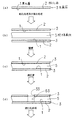
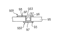
近年、プリント配線板のビアホールは、レーザー照射により形成する方法が開発されている。その形成方法を具体的に説明すると、図6に示すごとく、まず、絶縁基板95の表面に金属箔93を貼着し、ビアホール形成部分にエッチングにより予め開口孔933を形成する。
次いで、開口孔933内にレーザーを照射して絶縁基板95のビアホール形成部分を、その高いエネルギーにより焼失させる。そして、レーザーが、底部を形成する金属箔93に到達したときにレーザー照射を停止し、ビアホール96の穿設を完了する。次いで、ビアホール96内部に金属めっき膜97を形成して、ビアホール96に電気的導通性を付与する。
その後、金属箔93にエッチングを施して導体パターン931、932を形成すると、プリント配線板が得られる(特許文献参照)。
In recent years, methods for forming via holes in printed wiring boards by laser irradiation have been developed. More specifically, as shown in FIG. 6, first, a
Next, a laser is irradiated into the
Thereafter, when the
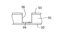
しかしながら、上記従来のレーザー照射によるビアホール形成方法においては、図7に示すごとく、ビアホール96内部に絶縁基板95の残さ94が残る。この残さ94は、図6に示すごとく、ビアホール96内における金属めっき膜97の形成を妨げる。また、金属箔93と金属めっき膜97との密着性を低下させる。そのため、ビアホール96の導通信頼性が低くなる。
However, in the conventional via hole forming method by laser irradiation, the
そこで、かかるビアホール96内の残さ94を除去するために、ビアホール96内にデスミア処理を施すことが行われている。
しかし、デスミア処理が不十分などの場合に、残さが十分に除去されない場合がある。そのため、依然として、ビアホールの導通信頼性は十分なものとはいえない。
Therefore, in order to remove the
However, when the desmear process is insufficient, the residue may not be sufficiently removed. Therefore, the via hole conduction reliability is still not sufficient.
本発明はかかる従来の問題点に鑑み、ビアホールの導通信頼性が高いプリント配線板の製造方法を提供しようとするものである。 In view of the conventional problems, the present invention intends to provide a method for manufacturing a printed wiring board having high via hole conduction reliability.
本発明は、金属箔に黒化層を形成する工程と、
前記黒化層を絶縁基板の両面に対面させ、前記金属箔を上下から貼着する工程と、
前記絶縁基板のビアホール形成部分にレーザーを照射して、前記絶縁基板の下方に貼着された金属箔を底部とするビアホールを形成する工程と、
前記ビアホール内部の残さを除去するデスミア処理工程と、
前記各金属箔表面を0.1〜2μmの厚み範囲で除去するソフトエッチング工程と、
前記ビアホール底部の金属箔表面に黒化層のないことを光学的手段によって確認してから、前記ビアホール内部を含めて前記各金属箔表面に金属めっき膜を形成する工程と、
前記金属箔をエッチングして前記絶縁基板の両面に導体パターンを形成する工程と、
を含むことを特徴とするプリント配線板の製造方法である。
The present invention includes a step of forming a blackened layer on a metal foil;
A step of facing the blackening layer on both sides of the insulating substrate, and attaching the metal foil from above and below;
Irradiating the via hole forming part of the insulating substrate with a laser to form a via hole having a metal foil attached to the bottom of the insulating substrate as a bottom; and
A desmear treatment step for removing a residue inside the via hole;
A soft etching step of removing the surface of each metal foil in a thickness range of 0.1 to 2 μm;
After confirming by optical means that there is no blackening layer on the metal foil surface at the bottom of the via hole, forming a metal plating film on each metal foil surface including the inside of the via hole;
Etching the metal foil to form a conductor pattern on both sides of the insulating substrate;
The printed wiring board manufacturing method characterized by including.
本発明において最も注目すべきことは、金属箔の絶縁基板と対向する側の表面に黒化層を形成することによりビアホール底部に黒化層を配置させること、ビアホール内部にデスミア処理を施した後にソフトエッチングを行い金属箔表面の黒化層を除去することである。 What should be noted most in the present invention is that a blackened layer is formed at the bottom of the via hole by forming a blackened layer on the surface of the metal foil facing the insulating substrate, and after the desmear treatment is performed inside the via hole. Soft etching is performed to remove the blackened layer on the surface of the metal foil.
デスミア処理によって、ビアホール内部に残った絶縁基板の残さが除去されるが、デスミア処理が不十分で残さがビアホール底部の金属箔に残存している場合には、ソフトエッチングによって金属箔表面がエッチングされず、残さ付着部分の黒化層が残ることになる。残った黒化層の有無を検査することにより、ビアホール底部に残さが付着しているか否かを検査できる。残さのないものについて後工程である金属めっき膜を形成することにより、ビアホール底部に金属めっき膜が強固に密着し、ビアホールの導通信頼性が高いプリント配線板が得られる。 The desmear process removes the insulating substrate remaining inside the via hole, but if the desmear process is insufficient and the residue remains on the metal foil at the bottom of the via hole, the surface of the metal foil is etched by soft etching. Therefore, the blackened layer of the remaining adhered portion remains. By inspecting the presence or absence of the remaining blackened layer, it is possible to inspect whether or not the residue is attached to the bottom of the via hole. By forming a metal plating film, which is a subsequent process, for those that do not have a residue, the metal plating film adheres firmly to the bottom of the via hole, and a printed wiring board with high via hole conduction reliability is obtained.
一方、ビアホール内の残さによってソフトエッチング後に黒化層が残ったものは、検査時に不良品とし、再度ビアホール内にデスミア処理を施すかまたは廃棄等をする。不良品のものをビアホール内部のデスミア処理を行わないで、後の金属めっき膜形成を行うと、残さが金属箔と金属めっき膜との密着性及び導通性を妨げ、ビアホールの導通信頼性が低下することがある。 On the other hand, if the blackened layer remains after the soft etching due to the residue in the via hole, it is regarded as a defective product at the time of inspection, and desmear processing is again performed or discarded in the via hole. If a defective product is not subjected to desmear treatment inside the via hole and a subsequent metal plating film is formed, the residue prevents the adhesion and conductivity between the metal foil and the metal plating film, and the via hole conduction reliability decreases. There are things to do.
また、ビアホールは、レーザーにより穿設しているため、微小な孔に形成できる。そのため、絶縁基板の高密度実装化を実現できる。
更に、金属箔における絶縁基板に対向する側の表面には黒化層が形成されるため、金属箔と絶縁基板との接着性が高い。従って、金属箔のエッチングにより形成される導体パターンは、絶縁基板に対して優れた接着性を有することになる。
Further, since the via hole is formed by a laser, it can be formed into a minute hole. Therefore, high-density mounting of the insulating substrate can be realized.
Furthermore, since the blackened layer is formed on the surface of the metal foil facing the insulating substrate, the adhesion between the metal foil and the insulating substrate is high. Therefore, the conductor pattern formed by etching the metal foil has excellent adhesion to the insulating substrate.
上記金属箔としては、たとえば、銅箔などを用いる。
上記絶縁基板としては、たとえば、ガラスエポキシ基板、ガラスポリイミド基板、ガラスビスマレイミドトリアジン基板等を用いる。
上記絶縁基板は、予め内部に1層又は2層以上の導体パターンが形成されていてもよい。
上記黒化層は、例えば、金属箔にリン酸ナトリウム溶液などの薬品による黒化処理によって形成される、黒色の層をいう。
As said metal foil, copper foil etc. are used, for example.
As the insulating substrate, for example, a glass epoxy substrate, a glass polyimide substrate, a glass bismaleimide triazine substrate or the like is used.
The insulating substrate may have a conductor pattern of one layer or two or more layers formed therein in advance.
The blackening layer refers to a black layer formed on a metal foil by a blackening treatment using a chemical such as a sodium phosphate solution.
デスミア処理とは、濃硫酸、クロム酸又はこれらの混酸、あるいは過マンガン酸ナトリウム又は過マンガン酸カリウムの溶液に、ビアホールを形成した絶縁基板を浸漬し、ビアホール内の残さを溶解除去する化学薬品処理法をいう。 Desmear treatment is a chemical treatment that dissolves and removes the residue in the via hole by immersing the insulating substrate in which the via hole is formed in concentrated sulfuric acid, chromic acid or a mixed acid thereof, or a solution of sodium permanganate or potassium permanganate. Say the law.
ソフトエッチングとは、ビアホール底部に露出した金属箔表面を化学反応によりわずかに溶解除去することをいう。ソフトエッチングによる金属箔の溶解除去厚みは、0.1〜2μmである。0.1μm未満の場合には、金属箔表面に絶縁基板の残さが残っていなくても金属箔表面の黒化層を除去できない部分が残るおそれがあり、残さの有無を正確に判断できないおそれがある。また、2μmを超える場合には、ソフトエッチングの工程費が高くなるおそれがある。 Soft etching means that the surface of the metal foil exposed at the bottom of the via hole is slightly dissolved and removed by a chemical reaction. The thickness of the metal foil dissolved and removed by soft etching is 0.1 to 2 μm. If the thickness is less than 0.1 μm, there may be a portion where the blackened layer on the surface of the metal foil cannot be removed even if there is no residue of the insulating substrate on the surface of the metal foil. is there. On the other hand, when the thickness exceeds 2 μm, the process cost of soft etching may be increased.
ビアホール内への金属めっき膜の形成は、化学めっきにより行う。化学めっき後に更に電気めっきを行うことが好ましい。これにより、金属めっき膜を膜厚に形成でき、ビアホールの電気導通性が向上する。金属めっき膜は、たとえば、銅、ニッケル、金などの金属からなる。 The metal plating film is formed in the via hole by chemical plating. It is preferable to further perform electroplating after chemical plating. Thereby, a metal plating film can be formed in a film thickness and the electrical conductivity of a via hole is improved. A metal plating film consists of metals, such as copper, nickel, and gold, for example.
上記黒化層を形成する前に、上記金属箔の絶縁基板に対向する側の表面に、粗化処理を施すことが好ましい。粗化処理により金属箔表面が粗化面となる。金属箔と絶縁基板とを接着したときには、この粗化面に絶縁基板材料が食い込み、金属箔と絶縁基板との接着性が高くなる。そのため、導体パターンが絶縁基板に対して、さらに強固に接着することになる。 Before forming the blackening layer, it is preferable to subject the surface of the metal foil facing the insulating substrate to a roughening treatment. The surface of the metal foil becomes a roughened surface by the roughening treatment. When the metal foil and the insulating substrate are bonded, the insulating substrate material bites into the roughened surface, and the adhesion between the metal foil and the insulating substrate is increased. Therefore, the conductor pattern is more firmly bonded to the insulating substrate.
また、ビアホール底部に露出した金属箔表面も粗化面となり、金属めっき膜との接着性が高くなる。
粗化処理とは、金属箔の表面を粗化面とする処理をいい、その具体例としては例えば、ジェットスクラブなどの物理的処理、化学処理がある。化学処理の概念には黒化処理が含まれることもあるが、本発明においては化学処理は黒化処理を含めないこととする。
Further, the surface of the metal foil exposed at the bottom of the via hole also becomes a roughened surface, and the adhesion with the metal plating film is enhanced.
The roughening treatment refers to a treatment in which the surface of the metal foil is roughened, and specific examples thereof include physical treatment such as jet scrub and chemical treatment. Although the concept of chemical treatment may include blackening treatment, in the present invention, chemical treatment does not include blackening treatment.
次に、参考までに、他のプリント配線板の製造方法として、絶縁基板におけるビアホール形成部分の底部に、金属箔を貼着する工程と、
上記絶縁基板のビアホール形成部分にレーザーを照射して、上記金属箔を底部とするビアホールを形成する工程と、
上記ビアホール底部に露出した金属箔にデスミア処理を施す工程と、
ビアホール底部に露出した金属箔にニッケルめっきの光沢層を形成する工程と、
ビアホール底部の金属箔表面に光沢層が均一に形成されていることを確認する工程と、
ビアホール内部に金属めっき膜を形成する工程と、
上記金属箔にエッチングを施して導体パターンを形成する工程とからなることを特徴とするプリント配線板の製造方法がある。
Next, for reference, as another printed wiring board manufacturing method, a step of attaching a metal foil to the bottom of the via hole forming portion in the insulating substrate,
Irradiating the via hole forming portion of the insulating substrate with a laser to form a via hole having the metal foil as a bottom; and
Applying a desmear treatment to the metal foil exposed at the bottom of the via hole;
Forming a bright layer of nickel plating on the metal foil exposed at the bottom of the via hole;
A step of confirming that a gloss layer is uniformly formed on the metal foil surface at the bottom of the via hole;
Forming a metal plating film inside the via hole;
There is a method for manufacturing a printed wiring board, which includes a step of etching the metal foil to form a conductor pattern.
該参考製造方法は、絶縁基板に、ビアホールを形成しデスミア処理をした後、その底部に露出した金属箔にニッケルめっきの光沢層を形成している点が、上記本発明の製造方法と相違する。 The reference manufacturing method is different from the manufacturing method of the present invention described above in that a via hole is formed in an insulating substrate and desmear treatment is performed, and then a nickel plating gloss layer is formed on the metal foil exposed at the bottom. .
この参考製造方法では、ビアホール内部にデスミア処理をした後に絶縁基板の残さがすべて除去された場合には、ビアホール底部に露出した金属箔表面の全体に均一に光沢層が形成され、均一な光沢を発する。一方、残っていた場合には、残さの付着部分には光沢層は形成されず、底部全体が不均一な光沢を発する。 In this reference manufacturing method, when all the residue of the insulating substrate is removed after the desmear treatment inside the via hole, the gloss layer is uniformly formed on the entire surface of the metal foil exposed at the bottom of the via hole, and the uniform gloss is obtained. To emit. On the other hand, when it remains, a glossy layer is not formed on the adhered portion of the residue, and the entire bottom emits uneven gloss.
そこで、このビアホール底部の光沢の状態を検査することにより、底部に絶縁基板の残さが残っているかいないかを検査できる。すなわち、残さが残っていない場合には、底部全体が均一な光沢を発し、残さが残っていた場合には不均一な光沢を発する。 Therefore, by inspecting the glossy state of the bottom of the via hole, it is possible to inspect whether or not the insulating substrate remains on the bottom. That is, when no residue remains, the entire bottom portion emits a uniform gloss, and when the residue remains, a non-uniform gloss is emitted.
よって、底部が均一な光沢を発するビアホールを有する絶縁基板について、後工程のソフトエッチング及び金属めっき膜形成を行う。これにより、ビアホール底部の金属箔と金属めっき膜との密着性が向上し、導通信頼性が高いビアホールを有するプリント配線板を得ることができる。 Therefore, post-process soft etching and metal plating film formation are performed on an insulating substrate having a via hole with a uniform gloss at the bottom. Thereby, the adhesiveness of the metal foil and metal plating film of a via-hole bottom part improves, and the printed wiring board which has a via hole with high conduction | electrical_connection reliability can be obtained.
一方、底部が不均一な光沢を発するビアホールを有する絶縁基板については、上記の本発明の製造方法で説明したと同様に、検査時に不良品とし、後工程を行わない。 On the other hand, an insulating substrate having a via hole that emits uneven gloss at the bottom is regarded as a defective product at the time of inspection as in the manufacturing method of the present invention, and no post-process is performed.
また、ビアホールは、レーザー照射により形成しているため、微小に形成できる。そのため、プリント配線板の高密度実装化が実現できる。
次に、本発明、又は参考製造方法によれば、例えば、絶縁基板と、該絶縁基板の表面に形成された導体パターンと、絶縁基板を貫通し上記金属箔を底部とするビアホールとからなり、かつ、上記ビアホールの底部に金属メッキ膜が形成されているプリント配線板が得られる。
Further, since the via hole is formed by laser irradiation, it can be formed minutely. Therefore, high-density mounting of the printed wiring board can be realized.
Next, according to the present invention or the reference manufacturing method, for example, an insulating substrate, a conductive pattern formed on the surface of the insulating substrate, and a via hole penetrating the insulating substrate and having the metal foil as a bottom, And the printed wiring board by which the metal plating film is formed in the bottom part of the said via hole is obtained.
また、本発明の方法により得られるプリント配線板は、導体パターンの表面に黒化層が形成されているため、絶縁基板に対する接着性が高い。また、上記の製造方法で説明したと同様の効果を発揮できる。 Moreover, since the blackened layer is formed in the surface of a conductor pattern, the printed wiring board obtained by the method of this invention has high adhesiveness with respect to an insulated substrate. Moreover, the same effect as demonstrated by said manufacturing method can be exhibited.
また、上記黒化層は、絶縁基板の粗化面表面に形成されていることが好ましい。導体パターンの粗化面には、絶縁基板の材料が食い込むため、強固に接着することになるためである。
その他は、上記の製造方法と同様である。
なお、本発明のプリント配線板の表面には、さらに1層又は2層以上の導体パターンを積層してもよい。
The blackened layer is preferably formed on the roughened surface of the insulating substrate. This is because the material of the insulating substrate bites into the roughened surface of the conductor pattern, so that it is firmly bonded.
Others are the same as that of said manufacturing method.
In addition, you may laminate | stack the conductor pattern of 1 layer or 2 layers or more on the surface of the printed wiring board of this invention.
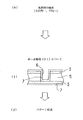
実施形態例1
本発明の実施形態例にかかるプリント配線板及びその製造方法について、図1〜図3を用いて説明する。
本例のプリント配線板は、図3(j)に示すごとく、絶縁基板5と、絶縁基板5の表面に形成された導体パターン31、32と、絶縁基板5を貫通し導体パターン32を底部とするビアホール6とからなる。導体パターン31、32における絶縁基板5と接着される側の表面には、黒化層1が形成されている。黒化層1は、絶縁基板5の粗化面2に形成されている。
A printed wiring board and a manufacturing method thereof according to an embodiment of the present invention will be described with reference to FIGS.
As shown in FIG. 3 (j), the printed wiring board of this example has an insulating
次に、プリント配線板の製造方法について説明する。
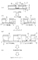
まず、図1(a)に示すごとく、金属箔3における絶縁基板5に対向する側の表面に、粗化処理を施して、粗化面2を形成する。金属箔3としては、銅箔を用いる。金属箔3の大きさは、後述する絶縁基板とほぼ同一の大きさとする。
Next, the manufacturing method of a printed wiring board is demonstrated.
First, as shown in FIG. 1A, a roughened
次に、金属箔3の粗化面2に黒化層1を形成する。
次に、図1(b)に示すごとく、絶縁基板5として、Bステージのエポキシ樹脂とガラスクロスとからなるプリプレグを準備し、この絶縁基板5の両面に金属箔3を積層する。
次いで、図1(c)に示すごとく、積層された絶縁基板5及び金属箔3を熱圧着する。このとき、黒化層1は、金属箔3におけるビアホールの開口部となる部分に対面することになる。
Next, the blackened
Next, as shown in FIG. 1B, a prepreg made of B-stage epoxy resin and glass cloth is prepared as the insulating
Next, as shown in FIG. 1C, the laminated insulating
次に、図1(d)に示すごとく、レーザー照射側、即ち上方の金属箔3にエッチングを施して、金属箔3おけるビアホール形成部分63を被覆する部分に、開口孔33を形成する。一方、レーザー照射側と反対側、即ち下方の金属箔3には、そのビアホール形成部分63を被覆する部分は、開口孔を形成しないでおく。
Next, as shown in FIG. 1D, etching is performed on the
次に、図2(e)に示すごとく、上方の金属箔3の開口孔33にレーザー8を照射して、絶縁基板5のビアホール形成部分63に孔あけをする。レーザーによる孔あけは、ビアホール形成部分の底部を被覆する金属箔3表面において停止する。これにより、下方の金属箔3を底部とするビアホール6が形成される。
Next, as shown in FIG. 2 (e), a laser 8 is irradiated to the
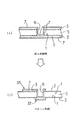
次に、図2(f)に示すごとく、ビアホール6底部に露出した金属箔3にデスミア処理を施す。デスミア処理は、過マンガン酸溶液に絶縁基板5を浸漬することにより行う。これにより、図2(f1)に示すごとく、ビアホール6内に付着していた絶縁基板5の残さ4は除去される。一方、デスミア処理が不十分の場合には、図2(f2)に示すごとく、ビアホール6内に残さ4が残る。
Next, as shown in FIG. 2 (f), desmear treatment is performed on the
次に、図2(g)に示すごとく、ビアホール6底部に露出した金属箔3にソフトエッチングを行う。これにより、図2(g1)に示すごとく、ビアホール6底部に露出した金属箔3表面から、黒化層が除去される。一方、図2(g2)に示すごとく、絶縁基板の残さが残っている場合には、残さ4が付着している部分の黒化層1は除去されない。
Next, as shown in FIG. 2G, the
次に、図2(h)に示すごとく、ビアホール6の底部の金属箔3表面に黒化層のないことを確認する。具体的には、顕微鏡等の光学的手段により、ビアホール底部に黒化層が残っているか否かを検査する。
Next, as shown in FIG. 2 (h), it is confirmed that there is no blackened layer on the surface of the
次に、図3(i)に示すごとく、ビアホール底部に黒化層が残っていない絶縁基板5(図2(g1))について、金属めっき処理を行う。具体的には、ビアホール6内部を含めて金属箔3の表面全体に化学銅めっき、電気銅めっきを行い、金属めっき膜7を形成する。
Next, as shown in FIG. 3I, a metal plating process is performed on the insulating substrate 5 (FIG. 2G1) in which the blackened layer does not remain at the bottom of the via hole. Specifically, chemical copper plating and electrolytic copper plating are performed on the entire surface of the
次に、図3(j)に示すごとく、絶縁基板5表面の金属箔3にエッチングを施して、導体パターン31、32を形成する。
以上により、プリント配線板が得られる。
Next, as shown in FIG. 3 (j), the
Thus, a printed wiring board is obtained.
一方、図2(g2)に示すごとく、ビアホール内の残さ4によってソフトエッチング後に黒化層1が残ったものは、検査時に不良品とし、再度ビアホール内にデスミア処理を施すかまたは廃棄等をする。不良品のものをビアホール内部のデスミア処理を行わないで、後の金属めっき膜形成を行うと、残さが金属箔と金属めっき膜との密着性及び導通性を妨げ、ビアホールの導通信頼性が低下することがある。
On the other hand, as shown in FIG. 2 (g2), the blackened
次に、本例の作用及び効果について説明する。
本例においては、金属箔3の絶縁基板5と対向する側の表面に黒化層1を形成することによりビアホール6底部に黒化層1を配置させ(図2(e))、ビアホール6内部にデスミア処理を施した(図2(f))後にソフトエッチングを行い金属箔表面の黒化層を除去している(図2(g))。
Next, the operation and effect of this example will be described.
In this example, the blackened
デスミア処理によって、ビアホール内部に残った絶縁基板の残さが除去され、ソフトエッチングを行うことにより、図2(g1)に示すごとく、ビアホール5底部の金属箔3表面の黒化層1が除去される。
しかし、デスミア処理不十分で残さがビアホール底部の金属箔に残存している場合には、図2(g2)に示すごとく、ソフトエッチングによって金属箔3表面の黒化層1がエッチングされず、残さ4が付着している部分の黒化層1が残ることになる。
By the desmear process, the insulating substrate remaining inside the via hole is removed, and by performing soft etching, the blackened
However, when the desmear treatment is insufficient and the residue remains on the metal foil at the bottom of the via hole, the blackened
そこで、図2(h)に示すごとく、残った黒化層の有無を検査することにより、ビアホール底部に残さが付着しているか否かを検査できる。
そして、図3(i)に示すごとく、ビアホール底部に残さのない絶縁基板について後工程である金属めっき膜7を形成することにより、ビアホール6底部に金属めっき膜7が強固に密着し、ビアホール6の導通信頼性が高いプリント配線板が得られる。
Therefore, as shown in FIG. 2H, it is possible to inspect whether or not the residue is attached to the bottom of the via hole by inspecting the presence or absence of the remaining blackened layer.
Then, as shown in FIG. 3 (i), by forming a
また、ビアホールは、レーザーにより穿設しているため、微小な孔に形成できる。そのため、絶縁基板の高密度実装化を実現できる。
更に、図3(j)に示すごとく、金属箔3における絶縁基板5に対向する側の表面には黒化層1が形成されるため、金属箔3と絶縁基板5との接着性が高い。従って、金属箔3のエッチングにより形成される導体パターン31、32は、絶縁基板5に対して優れた接着性を有することになる。
Further, since the via hole is formed by a laser, it can be formed into a minute hole. Therefore, high-density mounting of the insulating substrate can be realized.
Further, as shown in FIG. 3 (j), since the
また、図1(a)に示すごとく、金属箔3の絶縁基板5に対向する側の表面に、粗化処理を施している。このため、金属箔3と絶縁基板5との接着したときには、粗化面2に絶縁基板5の材料が食い込み、金属箔3と絶縁基板5との接着性が高くなる。そのため、図3(j)に示すごとく、導体パターン31、32が絶縁基板5に対して、さらに強固に接着することになる。
Further, as shown in FIG. 1A, the surface of the
参考実施形態例
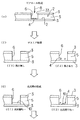
本例のプリント配線板の製造方法は、実施形態例1のように貼着前に金属箔に予め黒化層を形成する代わりに、図4(e)、(f)に示すごとく、ビアホール6を形成しデスミア処理をした後、図4(G)に示すごとく、その底部に露出した金属箔3にニッケルめっきの光沢層10を形成している。
Reference Embodiment Example The printed wiring board manufacturing method of this example is shown in FIGS. 4 (e) and 4 (f) instead of forming a blackened layer on the metal foil in advance before sticking as in the first embodiment. As shown in FIG. 4G, after the via
即ち、まず、金属箔における絶縁基板と対向する側と反対側の表面に、粗化面を形成する。次いで、この粗化面に黒化層を形成することなく、金属箔を絶縁基板の上下面に積層し、熱圧着し、ビアホール形成部分を被覆する部分に開口孔を形成する(図1(a)〜図1(d)参照)。 That is, first, a roughened surface is formed on the surface of the metal foil opposite to the side facing the insulating substrate. Next, without forming a blackened layer on the roughened surface, a metal foil is laminated on the upper and lower surfaces of the insulating substrate, thermocompression bonded, and an opening is formed in a portion covering the via hole forming portion (FIG. 1 (a)). ) To FIG. 1 (d)).
次に、図4(e)に示すごとく、金属箔3の開口孔33内に露出した絶縁基板5にレーザー8を照射して、金属箔3を底部とするビアホール6を形成する。
次に、図4(f)に示すごとく、デスミア処理を行う。これにより、図4(f1)に示すごとく、ビアホール6の底部に付着していた絶縁基板の残さが除去される。一方、デスミア処理が不十分である場合には、図4(f2)に示すごとく、ビアホール6の底部に残さ4が残る。
Next, as shown in FIG. 4E, the insulating
Next, desmear processing is performed as shown in FIG. As a result, as shown in FIG. 4F1, the residue of the insulating substrate attached to the bottom of the via
次に、図4(G)に示すごとく、ビアホール6の底部に光沢層10を形成する。このとき、残さが除去されたビアホール6の中には、図4(G1)に示すごとく、光沢層10が均一に形成される。一方、残さ4が残っている場合には、図4(G2)に示すごとく、光沢層10が不均一に形成されることになる。
Next, as shown in FIG. 4G, the
次に、図5(h)に示すごとく、ビアホール内の光沢層の形成状態を、顕微鏡などの光学的手段により検査する。図4(G1)に示すごとく、光沢層が均一に形成されている場合には、均一な光沢を発する。一方、図4(G2)に示すごとく、光沢層が不均一に形成されている場合には、不均一な光沢を発する。 Next, as shown in FIG. 5H, the formation state of the gloss layer in the via hole is inspected by an optical means such as a microscope. As shown in FIG. 4 (G1), when the gloss layer is formed uniformly, uniform gloss is emitted. On the other hand, as shown in FIG. 4 (G2), when the gloss layer is formed non-uniformly, non-uniform gloss is emitted.
次に、図5(i)に示すごとく、絶縁基板に、化学銅めっき処理及び電気銅めっき処理を施して、ビアホールの内部に金属めっき膜7を形成する。その後、図5(j)に示すごとく、金属箔3にエッチングを施して、導体パターンを形成する(図3(j)参照)。以上によりプリント配線板が得られる。
Next, as shown in FIG. 5I, the insulating substrate is subjected to chemical copper plating and electrolytic copper plating to form a
本例においては、図4(f1)に示すごとくビアホール内部にデスミア処理をした後に絶縁基板の残さがすべて除去された場合には、図4(G1)に示すごとくビアホール6底部に露出した金属箔3表面の全体に均一に光沢層10が形成される。一方、図4(f2)に示すごとく残さ4が残っていた場合には、図4(G2)に示すごとくビアホール6底部に残った残さ4の付着部分には光沢層10は形成されない。
In this example, as shown in FIG. 4 (f1), when all of the insulating substrate residue is removed after the desmear process inside the via hole, the metal foil exposed at the bottom of the via
従って、図5(h)に示すごとく、ビアホール6底部の光沢の状態を検査することにより、底部に絶縁基板の残さが残っているかいないかを検査できる。すなわち、残さが残っていない場合には、底部全体が均一な光沢を発し、残さが残っていた場合には不均一な光沢を発する。
Therefore, as shown in FIG. 5H, it is possible to inspect whether or not the insulating substrate remains on the bottom by inspecting the glossy state of the bottom of the via
そして、底部が均一な光沢を発するビアホール6を有する絶縁基板5について、後工程の金属めっき膜形成(図5(i))を行う。これにより、ビアホール6底部の金属箔3と金属めっき膜7との密着性が向上し、導通信頼性が高いビアホール6を有するプリント配線板を得ることができる。
Then, a post-process metal plating film formation (FIG. 5 (i)) is performed on the insulating
一方、底部が不均一な光沢を発するビアホールを有する絶縁基板については、上記の第1の製造方法で説明したと同様に、検査時に不良品とし、後工程を行わない。 On the other hand, an insulating substrate having a via hole that emits uneven luster at the bottom is regarded as a defective product at the time of inspection, as described in the first manufacturing method, and no subsequent process is performed.
また、ビアホールは、レーザー照射により形成しているため、微小に形成できる。そのため、プリント配線板の高密度実装化が実現できる。 Further, since the via hole is formed by laser irradiation, it can be formed minutely. Therefore, high-density mounting of the printed wiring board can be realized.
1...黒化層、
10...光沢層、
2...粗化面、
3...金属箔、
31、32...導体パターン、
33...開口孔、
4...残さ、
5...絶縁基板、
6...ビアホール、
63...ビアホール形成部分、
7...金属めっき膜、
8...レーザー、
1. . . Blackening layer,
10. . . Glossy layer,
2. . . Roughened surface,
3. . . Metal foil,
31, 32. . . Conductor pattern,
33. . . Opening hole,
4). . . The rest,
5). . . Insulating substrate,
6). . . Beer hall,
63. . . Via hole formation part,
7). . . Metal plating film,
8). . . laser,
Claims (1)
前記黒化層を絶縁基板の両面に対面させ、前記金属箔を上下から貼着する工程と、
前記絶縁基板のビアホール形成部分にレーザーを照射して、前記絶縁基板の下方に貼着された金属箔を底部とするビアホールを形成する工程と、
前記ビアホール内部の残さを除去するデスミア処理工程と、
前記各金属箔表面を0.1〜2μmの厚み範囲で除去するソフトエッチング工程と、
前記ビアホール底部の金属箔表面に黒化層のないことを光学的手段によって確認してから、前記ビアホール内部を含めて前記各金属箔表面に金属めっき膜を形成する工程と、
前記金属箔をエッチングして前記絶縁基板の両面に導体パターンを形成する工程と、
を含むことを特徴とするプリント配線板の製造方法。 Forming a blackened layer on the metal foil;
A step of facing the blackening layer on both sides of the insulating substrate, and attaching the metal foil from above and below;
Irradiating the via hole forming part of the insulating substrate with a laser to form a via hole having a metal foil attached to the bottom of the insulating substrate as a bottom; and
A desmear treatment step for removing a residue inside the via hole;
A soft etching step of removing the surface of each metal foil in a thickness range of 0.1 to 2 μm;
After confirming by optical means that there is no blackening layer on the metal foil surface at the bottom of the via hole, forming a metal plating film on each metal foil surface including the inside of the via hole;
Etching the metal foil to form a conductor pattern on both sides of the insulating substrate;
The printed wiring board manufacturing method characterized by including this.
Priority Applications (1)
| Application Number | Priority Date | Filing Date | Title |
|---|---|---|---|
| JP2005196437A JP2005294873A (en) | 2005-07-05 | 2005-07-05 | Method of manufacturing printed wiring board |
Applications Claiming Priority (1)
| Application Number | Priority Date | Filing Date | Title |
|---|---|---|---|
| JP2005196437A JP2005294873A (en) | 2005-07-05 | 2005-07-05 | Method of manufacturing printed wiring board |
Related Parent Applications (1)
| Application Number | Title | Priority Date | Filing Date |
|---|---|---|---|
| JP10363598A Division JP3716613B2 (en) | 1998-03-30 | 1998-03-30 | Printed wiring board and manufacturing method thereof |
Publications (1)
| Publication Number | Publication Date |
|---|---|
| JP2005294873A true JP2005294873A (en) | 2005-10-20 |
Family
ID=35327381
Family Applications (1)
| Application Number | Title | Priority Date | Filing Date |
|---|---|---|---|
| JP2005196437A Pending JP2005294873A (en) | 2005-07-05 | 2005-07-05 | Method of manufacturing printed wiring board |
Country Status (1)
| Country | Link |
|---|---|
| JP (1) | JP2005294873A (en) |
Cited By (2)
| Publication number | Priority date | Publication date | Assignee | Title |
|---|---|---|---|---|
| JP2009200236A (en) * | 2008-02-21 | 2009-09-03 | Daisho Denshi Co Ltd | Board with contact terminal, ic memory card, and manufacturing method of board with contact terminal |
| KR20250010678A (en) | 2022-06-30 | 2025-01-21 | 다이요 홀딩스 가부시키가이샤 | Circuit board and method for manufacturing the same |
-
2005
- 2005-07-05 JP JP2005196437A patent/JP2005294873A/en active Pending
Cited By (2)
| Publication number | Priority date | Publication date | Assignee | Title |
|---|---|---|---|---|
| JP2009200236A (en) * | 2008-02-21 | 2009-09-03 | Daisho Denshi Co Ltd | Board with contact terminal, ic memory card, and manufacturing method of board with contact terminal |
| KR20250010678A (en) | 2022-06-30 | 2025-01-21 | 다이요 홀딩스 가부시키가이샤 | Circuit board and method for manufacturing the same |
Similar Documents
| Publication | Publication Date | Title |
|---|---|---|
| KR102518566B1 (en) | Printed wiring board and method for manufacturing same | |
| JP2014120756A (en) | Method of manufacturing printed circuit board | |
| JP4857433B2 (en) | Metal laminate, metal laminate manufacturing method and printed circuit board manufacturing method | |
| TWI487451B (en) | Manufacturing method of multilayer printed wiring board | |
| KR101553635B1 (en) | Method of manufacturing printed circuit board, and printed circuit board obtained using method of manufacturing printed circuit board | |
| US7992296B2 (en) | PCB and manufacturing method thereof | |
| JP2000036660A (en) | Manufacture of build-up multilayer interconnection board | |
| JP4082776B2 (en) | Method for manufacturing printed wiring board | |
| JP4624217B2 (en) | Circuit board manufacturing method | |
| JP2009123986A (en) | Multilayer circuit board manufacturing method | |
| KR100911204B1 (en) | Manufacturing method of build-up integrated circuit board | |
| US8191249B2 (en) | Method of manufacturing a printed circuit board | |
| JP3716613B2 (en) | Printed wiring board and manufacturing method thereof | |
| JP2005294873A (en) | Method of manufacturing printed wiring board | |
| JP5938948B2 (en) | Semiconductor chip mounting substrate and manufacturing method thereof | |
| JP2000036659A (en) | Manufacture of build-up multilayer interconnection board | |
| JP5298740B2 (en) | Multilayer circuit board manufacturing method | |
| KR20100109698A (en) | Method of manufacturing a printed circuit board | |
| JP5172565B2 (en) | Multilayer wiring board manufacturing method and multilayer wiring board | |
| KR20100021145A (en) | A multi layer fpcb for forming bvh by using pth and a method thereof | |
| JP2000036661A (en) | Manufacture of build-up multilayer interconnection board | |
| JP2000036662A (en) | Manufacture of build-up multilayer interconnection board | |
| JP2001203464A (en) | Buildup multilayer printed wiring board and its manufacturing method | |
| JP2002217536A (en) | Pretreatment method for plating non-through holes and through holes in printed wiring boards | |
| JP2005191115A (en) | Wiring board and manufacturing method thereof |
Legal Events
| Date | Code | Title | Description |
|---|---|---|---|
| A131 | Notification of reasons for refusal |
Effective date: 20080325 Free format text: JAPANESE INTERMEDIATE CODE: A131 |
|
| A521 | Written amendment |
Free format text: JAPANESE INTERMEDIATE CODE: A523 Effective date: 20080523 |
|
| A131 | Notification of reasons for refusal |
Effective date: 20080729 Free format text: JAPANESE INTERMEDIATE CODE: A132 |
|
| A02 | Decision of refusal |
Effective date: 20090113 Free format text: JAPANESE INTERMEDIATE CODE: A02 |