JP2005294845A - リソグラフィ装置、照明装置、及び強度分布を回転させるための光学要素 - Google Patents
リソグラフィ装置、照明装置、及び強度分布を回転させるための光学要素 Download PDFInfo
- Publication number
- JP2005294845A JP2005294845A JP2005105743A JP2005105743A JP2005294845A JP 2005294845 A JP2005294845 A JP 2005294845A JP 2005105743 A JP2005105743 A JP 2005105743A JP 2005105743 A JP2005105743 A JP 2005105743A JP 2005294845 A JP2005294845 A JP 2005294845A
- Authority
- JP
- Japan
- Prior art keywords
- lithographic apparatus
- intensity distribution
- optical element
- reflective
- radiation
- Prior art date
- Legal status (The legal status is an assumption and is not a legal conclusion. Google has not performed a legal analysis and makes no representation as to the accuracy of the status listed.)
- Granted
Links
Images
Classifications
-
- G—PHYSICS
- G03—PHOTOGRAPHY; CINEMATOGRAPHY; ANALOGOUS TECHNIQUES USING WAVES OTHER THAN OPTICAL WAVES; ELECTROGRAPHY; HOLOGRAPHY
- G03F—PHOTOMECHANICAL PRODUCTION OF TEXTURED OR PATTERNED SURFACES, e.g. FOR PRINTING, FOR PROCESSING OF SEMICONDUCTOR DEVICES; MATERIALS THEREFOR; ORIGINALS THEREFOR; APPARATUS SPECIALLY ADAPTED THEREFOR
- G03F7/00—Photomechanical, e.g. photolithographic, production of textured or patterned surfaces, e.g. printing surfaces; Materials therefor, e.g. comprising photoresists; Apparatus specially adapted therefor
- G03F7/70—Microphotolithographic exposure; Apparatus therefor
- G03F7/70058—Mask illumination systems
- G03F7/70091—Illumination settings, i.e. intensity distribution in the pupil plane or angular distribution in the field plane; On-axis or off-axis settings, e.g. annular, dipole or quadrupole settings; Partial coherence control, i.e. sigma or numerical aperture [NA]
- G03F7/70108—Off-axis setting using a light-guiding element, e.g. diffractive optical elements [DOEs] or light guides
-
- G—PHYSICS
- G03—PHOTOGRAPHY; CINEMATOGRAPHY; ANALOGOUS TECHNIQUES USING WAVES OTHER THAN OPTICAL WAVES; ELECTROGRAPHY; HOLOGRAPHY
- G03F—PHOTOMECHANICAL PRODUCTION OF TEXTURED OR PATTERNED SURFACES, e.g. FOR PRINTING, FOR PROCESSING OF SEMICONDUCTOR DEVICES; MATERIALS THEREFOR; ORIGINALS THEREFOR; APPARATUS SPECIALLY ADAPTED THEREFOR
- G03F7/00—Photomechanical, e.g. photolithographic, production of textured or patterned surfaces, e.g. printing surfaces; Materials therefor, e.g. comprising photoresists; Apparatus specially adapted therefor
- G03F7/70—Microphotolithographic exposure; Apparatus therefor
- G03F7/70058—Mask illumination systems
- G03F7/70091—Illumination settings, i.e. intensity distribution in the pupil plane or angular distribution in the field plane; On-axis or off-axis settings, e.g. annular, dipole or quadrupole settings; Partial coherence control, i.e. sigma or numerical aperture [NA]
- G03F7/701—Off-axis setting using an aperture
Landscapes
- Physics & Mathematics (AREA)
- General Physics & Mathematics (AREA)
- Exposure And Positioning Against Photoresist Photosensitive Materials (AREA)
- Exposure Of Semiconductors, Excluding Electron Or Ion Beam Exposure (AREA)
- Optical Elements Other Than Lenses (AREA)
Abstract
【解決手段】リソグラフィ投影装置は、長方形の断面を持つ反射型インテグレータを有する照明装置を含む。反射型インテグレータを出た強度分布を再分布させる光学要素が提供される。
【選択図】図1
Description
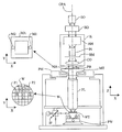
調整された放射投影ビームPB(例えばUV放射又はDUV放射、すなわち波長100〜400nm、例えば365、248、193又は157nmの電磁放射)を供給する照明装置(照明器)ILと、
パターン形成装置(例えばマスク又はレチクル)MAを支持する支持構造体(例えばマスク・テーブル)MTであって、部品PLに対してパターン形成装置を正確に配置する第1の位置決め手段PMに接続された支持構造体MTと、
基板(例えばレジストで被覆されたウェーハ)Wを保持する基板テーブル(例えばウェーハ・テーブル)WTであって、部品PLに対して基板を正確に配置する第2の位置決め手段PWに接続された基板テーブルWTと、
パターン形成装置MAによって投影ビームPBに付与されたパターンを、基板Wの(例えば1つ又は複数のダイを含む)標的部分Cに結像させる投影装置(例えば屈折投影レンズ)PLとを備えている。
SO 放射源
BD ビーム伝達装置
IL 照明装置(照明器)
AM 可調構成要素
IN インテグレータ
RM レチクル・マスキング装置
CO コンデンサ
PB 投影ビーム
MA パターン形成装置(マスク又はレクチル)
MT 支持構造体(マスク・テーブル)
PL 投影装置(レンズ)
W 基板(ウェーハ)
WT 基板テーブル(ウェーハ・テーブル)
C 標的部分
20、21 ひとみ平面
27a インカップリング・レンズ
27b アウトカップリング・レンズ
Claims (17)
- 調整された放射ビームを供給する照明装置を含むリソグラフィ装置において、該照明装置が、
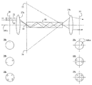
前記リソグラフィ装置の光軸に沿って配置され、該光軸に垂直な長方形の断面を有し、該断面が、互いに垂直なX軸及びY軸に平行な辺を有する反射型インテグレータと、
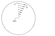
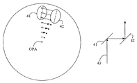
前記反射型インテグレータを出た強度分布を、前記X軸及びY軸のうちの少なくとも一方に関して非対称となるように再分布させるように構築され配置された光学要素とを含むリソグラフィ装置。 - 前記光学要素が、放射ビームの強度分布を、前記光軸を中心に5度〜85度の角度だけ回転させるように構築され配置されている請求項1に記載されたリソグラフィ装置。
- 前記角度が90/n度であり、nが2から18までの整数である請求項2に記載されたリソグラフィ装置。
- 前記光学要素が、前記反射型インテグレータの下流の前記照明装置のひとみ平面に配置されている請求項1に記載されたリソグラフィ装置。
- 前記光学要素が少なくとも1対の反射表面を含み、前記反射表面対が、前記ビームの強度分布の一部分を再分配するように構築され配置されている請求項4に記載されたリソグラフィ装置。
- 前記光学要素の上流での前記光軸と前記強度分布の前記一部分との間の距離が、前記光学要素の下流での前記距離に等しい請求項5に記載されたリソグラフィ装置。
- 前記反射表面が、被覆されたミラーを含む請求項5に記載されたリソグラフィ装置。
- 前記少なくとも1対の反射表面が平らで且つ互いに平行であり、それにより、前記光学要素の上流の前記放射ビームの放射線の方向が、前記光学要素の下流の前記放射線の方向に等しくなる請求項5に記載されたリソグラフィ装置。
- 前記少なくとも1対の反射表面が平らであり、前記照明装置の焦点面における前記ビームの対応する強度分布の中心が一致するように、一方の反射表面が他方の反射表面に対して所定の角度に配置されている請求項5に記載されたリソグラフィ装置。
- 前記光学要素が2対の反射表面を含み、反射表面対がそれぞれ、前記強度分布の2つのそれぞれの極の一方を再分配するように構築され配置されている請求項5に記載されたリソグラフィ装置。
- 前記光学要素が、前記放射ビームの強度分布の実質的に全体を回転させるように構築され配置された複数の反射表面対を含む請求項5に記載されたリソグラフィ装置。
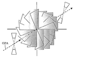
- 前記複数の反射表面対が放射状に延びる傾いたミラー・ブレードを含み、前記ミラー・ブレードが両面に反射被覆を含む請求項11に記載されたリソグラフィ装置。
- 前記ミラー・ブレードの厚さが、前記光軸からの距離及び前記光軸を中心とした角度の関数として変化している請求項12に記載されたリソグラフィ装置。
- 光軸に沿って配置され、該光軸に垂直な長方形の断面を有し、該断面が、互いに垂直なX軸及びY軸に平行な辺を有する反射型インテグレータと、
前記反射型インテグレータを出た強度分布が、前記X軸及びY軸の少なくとも一方に関して非対称となるように、強度分布を再分布させるように構築され配置された光学要素とを含む照明装置。 - 放射ビームの強度分布を5度〜85度の角度だけ回転させるように構築され配置された光学要素。
- 前記角度が可変であり、前記光学要素が前記角度の値に従って設定されるようになっている請求項14に記載された光学要素。
- 放射投影ビームを供給する照明装置と、
パターン形成装置を支持する支持構造体であって、該パターン形成装置がその断面パターンを前記投影ビームに付与する働きをするようになっている支持構造体と、
基板を保持する基板テーブルと、
パターンの付与された前記ビームを前記基板の標的部分に投影する投影装置とを含むリソグラフィ装置において、前記照明装置が、
前記リソグラフィ装置の光軸に沿って配置され、該光軸に垂直な長方形の断面を有し、該断面が互いに垂直なX軸及びY軸に平行な辺を有する反射型インテグレータと、
前記反射型インテグレータを出た強度分布が、前記X及びY軸の少なくとも一方に関して非対称となるように、強度分布を再分布させるように構築され配置された光学要素とを含むリソグラフィ装置。
Applications Claiming Priority (1)
| Application Number | Priority Date | Filing Date | Title |
|---|---|---|---|
| US10/816,170 US7312850B2 (en) | 2004-04-02 | 2004-04-02 | Lithographic apparatus, illumination system, and optical element for rotating an intensity distribution |
Publications (2)
| Publication Number | Publication Date |
|---|---|
| JP2005294845A true JP2005294845A (ja) | 2005-10-20 |
| JP4444869B2 JP4444869B2 (ja) | 2010-03-31 |
Family
ID=34887756
Family Applications (1)
| Application Number | Title | Priority Date | Filing Date |
|---|---|---|---|
| JP2005105743A Expired - Fee Related JP4444869B2 (ja) | 2004-04-02 | 2005-04-01 | リソグラフィ装置、照明装置、及び強度分布を回転させるための光学要素 |
Country Status (8)
| Country | Link |
|---|---|
| US (1) | US7312850B2 (ja) |
| EP (1) | EP1582931B1 (ja) |
| JP (1) | JP4444869B2 (ja) |
| KR (1) | KR100660504B1 (ja) |
| CN (1) | CN1684000A (ja) |
| DE (1) | DE602005007409D1 (ja) |
| SG (1) | SG115817A1 (ja) |
| TW (1) | TWI285788B (ja) |
Cited By (1)
| Publication number | Priority date | Publication date | Assignee | Title |
|---|---|---|---|---|
| KR20160120664A (ko) * | 2015-04-08 | 2016-10-18 | 캐논 가부시끼가이샤 | 조명 광학장치, 및 디바이스 제조 방법 |
Families Citing this family (3)
| Publication number | Priority date | Publication date | Assignee | Title |
|---|---|---|---|---|
| US7948606B2 (en) * | 2006-04-13 | 2011-05-24 | Asml Netherlands B.V. | Moving beam with respect to diffractive optics in order to reduce interference patterns |
| JP5319766B2 (ja) * | 2008-06-20 | 2013-10-16 | カール・ツァイス・エスエムティー・ゲーエムベーハー | マイクロリソグラフィ投影露光装置の光学系及びマイクロリソグラフィ露光方法 |
| CN109491213A (zh) * | 2018-12-04 | 2019-03-19 | 芯恩(青岛)集成电路有限公司 | 一种增加曝光强度的全反射积分器 |
Family Cites Families (22)
| Publication number | Priority date | Publication date | Assignee | Title |
|---|---|---|---|---|
| US5121160A (en) * | 1989-03-09 | 1992-06-09 | Canon Kabushiki Kaisha | Exposure method and apparatus |
| US6710855B2 (en) * | 1990-11-15 | 2004-03-23 | Nikon Corporation | Projection exposure apparatus and method |
| US5305054A (en) * | 1991-02-22 | 1994-04-19 | Canon Kabushiki Kaisha | Imaging method for manufacture of microdevices |
| US5815248A (en) * | 1993-04-22 | 1998-09-29 | Nikon Corporation | Illumination optical apparatus and method having a wavefront splitter and an optical integrator |
| GB9515328D0 (en) * | 1995-07-26 | 1995-09-20 | Willson Peter D W | Apparatus for modifying light quality:-diaphagm,colour changer and dimmer |
| KR970062816A (ko) * | 1996-02-13 | 1997-09-12 | 박병재 | 헤드 램프를 이용한 엔진룸 조사 장치 |
| US6144495A (en) | 1997-12-23 | 2000-11-07 | Canon Kabushiki Kaisha | Projection light source |
| US6231198B1 (en) * | 1998-02-17 | 2001-05-15 | Nikon Corporation | Reflective optical integrator |
| DE69931690T2 (de) * | 1998-04-08 | 2007-06-14 | Asml Netherlands B.V. | Lithographischer Apparat |
| JP3796369B2 (ja) * | 1999-03-24 | 2006-07-12 | キヤノン株式会社 | 干渉計を搭載した投影露光装置 |
| JP3710321B2 (ja) * | 1999-04-01 | 2005-10-26 | キヤノン株式会社 | 露光量制御方法、露光装置およびデバイス製造方法 |
| US6771350B2 (en) * | 2000-02-25 | 2004-08-03 | Nikon Corporation | Exposure apparatus and exposure method capable of controlling illumination distribution |
| JP2001264696A (ja) * | 2000-03-16 | 2001-09-26 | Canon Inc | 照明光学系及びそれを備えた露光装置 |
| DE10043315C1 (de) * | 2000-09-02 | 2002-06-20 | Zeiss Carl | Projektionsbelichtungsanlage |
| JP4401060B2 (ja) * | 2001-06-01 | 2010-01-20 | エーエスエムエル ネザーランズ ビー.ブイ. | リトグラフ装置、およびデバイス製造方法 |
| DE10132988B4 (de) * | 2001-07-06 | 2005-07-28 | Carl Zeiss Smt Ag | Projektionsbelichtungsanlage |
| TW554411B (en) * | 2001-08-23 | 2003-09-21 | Nikon Corp | Exposure apparatus |
| JP3826047B2 (ja) * | 2002-02-13 | 2006-09-27 | キヤノン株式会社 | 露光装置、露光方法、及びそれを用いたデバイス製造方法 |
| JP3661688B2 (ja) * | 2002-03-26 | 2005-06-15 | セイコーエプソン株式会社 | 照明装置 |
| JP2004063988A (ja) * | 2002-07-31 | 2004-02-26 | Canon Inc | 照明光学系、当該照明光学系を有する露光装置及びデバイス製造方法 |
| JP2005077964A (ja) * | 2003-09-03 | 2005-03-24 | Fujitsu Ltd | 分光装置 |
| US20050134820A1 (en) * | 2003-12-22 | 2005-06-23 | Asml Netherlands B.V. | Method for exposing a substrate, patterning device, and lithographic apparatus |
-
2004
- 2004-04-02 US US10/816,170 patent/US7312850B2/en not_active Expired - Fee Related
-
2005
- 2005-03-24 DE DE602005007409T patent/DE602005007409D1/de not_active Expired - Fee Related
- 2005-03-24 EP EP05251893A patent/EP1582931B1/en not_active Expired - Lifetime
- 2005-03-30 SG SG200501977A patent/SG115817A1/en unknown
- 2005-03-30 TW TW094110029A patent/TWI285788B/zh not_active IP Right Cessation
- 2005-04-01 KR KR1020050027421A patent/KR100660504B1/ko not_active Expired - Fee Related
- 2005-04-01 JP JP2005105743A patent/JP4444869B2/ja not_active Expired - Fee Related
- 2005-04-01 CN CNA2005100626251A patent/CN1684000A/zh active Pending
Cited By (3)
| Publication number | Priority date | Publication date | Assignee | Title |
|---|---|---|---|---|
| KR20160120664A (ko) * | 2015-04-08 | 2016-10-18 | 캐논 가부시끼가이샤 | 조명 광학장치, 및 디바이스 제조 방법 |
| JP2016200649A (ja) * | 2015-04-08 | 2016-12-01 | キヤノン株式会社 | 照明光学装置、およびデバイス製造方法 |
| KR102035163B1 (ko) | 2015-04-08 | 2019-10-22 | 캐논 가부시끼가이샤 | 조명 광학장치, 및 디바이스 제조 방법 |
Also Published As
| Publication number | Publication date |
|---|---|
| US20050219494A1 (en) | 2005-10-06 |
| SG115817A1 (en) | 2005-10-28 |
| EP1582931B1 (en) | 2008-06-11 |
| TWI285788B (en) | 2007-08-21 |
| KR100660504B1 (ko) | 2006-12-22 |
| JP4444869B2 (ja) | 2010-03-31 |
| EP1582931A1 (en) | 2005-10-05 |
| CN1684000A (zh) | 2005-10-19 |
| TW200600953A (en) | 2006-01-01 |
| DE602005007409D1 (de) | 2008-07-24 |
| US7312850B2 (en) | 2007-12-25 |
| KR20060045408A (ko) | 2006-05-17 |
Similar Documents
| Publication | Publication Date | Title |
|---|---|---|
| KR100563124B1 (ko) | 리소그래피 장치 | |
| KR101245785B1 (ko) | 조명 시스템 및 리소그래피 장치 | |
| US7126757B2 (en) | Illumination apparatus, exposure apparatus using the same, and device fabricating method | |
| US8426088B2 (en) | Method for a lithographic apparatus | |
| JP2008160109A (ja) | リソグラフィ装置および方法 | |
| JP5689461B2 (ja) | リソグラフィ装置、極端紫外線の反射を制御する方法、及びマスキングデバイス | |
| US9360762B2 (en) | Illumination system, lithographic apparatus and method | |
| KR101658494B1 (ko) | 반사성 요소의 어레이의 회전을 위한 마운팅 및 이를 포함하는 리소그래피 장치 | |
| KR100598643B1 (ko) | 디바이스 제조방법 | |
| JP2002353090A (ja) | 照明装置、露光装置、デバイス製造方法及びデバイス | |
| JP4999827B2 (ja) | リソグラフィ装置 | |
| JP2011187930A (ja) | リソグラフィ装置および方法 | |
| JP4444869B2 (ja) | リソグラフィ装置、照明装置、及び強度分布を回転させるための光学要素 | |
| US20050134820A1 (en) | Method for exposing a substrate, patterning device, and lithographic apparatus | |
| JP2005340847A (ja) | リソグラフィ装置およびデバイス製造方法 | |
| KR20090018149A (ko) | 광학 장치 | |
| JP2007194600A (ja) | リソグラフィ装置およびデバイス製造方法 | |
| JP5350504B2 (ja) | リソグラフィ装置及び方法 | |
| JP5390577B2 (ja) | リソグラフィ装置および方法 | |
| KR20040078902A (ko) | 메트롤로지의 라우팅 및 조종을 위한 디바이스 및 방법 | |
| JP2011150227A (ja) | 露光装置、およびデバイス製造方法 |
Legal Events
| Date | Code | Title | Description |
|---|---|---|---|
| RD03 | Notification of appointment of power of attorney |
Free format text: JAPANESE INTERMEDIATE CODE: A7423 Effective date: 20060904 |
|
| RD05 | Notification of revocation of power of attorney |
Free format text: JAPANESE INTERMEDIATE CODE: A7425 Effective date: 20070615 |
|
| A131 | Notification of reasons for refusal |
Free format text: JAPANESE INTERMEDIATE CODE: A131 Effective date: 20080527 |
|
| A521 | Request for written amendment filed |
Free format text: JAPANESE INTERMEDIATE CODE: A523 Effective date: 20080827 |
|
| A131 | Notification of reasons for refusal |
Free format text: JAPANESE INTERMEDIATE CODE: A131 Effective date: 20080926 |
|
| A521 | Request for written amendment filed |
Free format text: JAPANESE INTERMEDIATE CODE: A523 Effective date: 20081225 |
|
| TRDD | Decision of grant or rejection written | ||
| A01 | Written decision to grant a patent or to grant a registration (utility model) |
Free format text: JAPANESE INTERMEDIATE CODE: A01 Effective date: 20100104 |
|
| A01 | Written decision to grant a patent or to grant a registration (utility model) |
Free format text: JAPANESE INTERMEDIATE CODE: A01 |
|
| A61 | First payment of annual fees (during grant procedure) |
Free format text: JAPANESE INTERMEDIATE CODE: A61 Effective date: 20100114 |
|
| R150 | Certificate of patent or registration of utility model |
Free format text: JAPANESE INTERMEDIATE CODE: R150 |
|
| FPAY | Renewal fee payment (event date is renewal date of database) |
Free format text: PAYMENT UNTIL: 20130122 Year of fee payment: 3 |
|
| FPAY | Renewal fee payment (event date is renewal date of database) |
Free format text: PAYMENT UNTIL: 20140122 Year of fee payment: 4 |
|
| LAPS | Cancellation because of no payment of annual fees |