JP2005294814A - 半導体装置及びその作製方法 - Google Patents
半導体装置及びその作製方法 Download PDFInfo
- Publication number
- JP2005294814A JP2005294814A JP2005061959A JP2005061959A JP2005294814A JP 2005294814 A JP2005294814 A JP 2005294814A JP 2005061959 A JP2005061959 A JP 2005061959A JP 2005061959 A JP2005061959 A JP 2005061959A JP 2005294814 A JP2005294814 A JP 2005294814A
- Authority
- JP
- Japan
- Prior art keywords
- transistor
- insulating film
- gate electrode
- film
- active layer
- Prior art date
- Legal status (The legal status is an assumption and is not a legal conclusion. Google has not performed a legal analysis and makes no representation as to the accuracy of the status listed.)
- Granted
Links
- 239000004065 semiconductor Substances 0.000 title claims abstract description 167
- 238000004519 manufacturing process Methods 0.000 title claims abstract description 52
- 239000000758 substrate Substances 0.000 claims abstract description 104
- 238000000034 method Methods 0.000 claims abstract description 61
- 238000005530 etching Methods 0.000 claims description 77
- 238000007667 floating Methods 0.000 claims description 60
- VYPSYNLAJGMNEJ-UHFFFAOYSA-N silicon dioxide Inorganic materials O=[Si]=O VYPSYNLAJGMNEJ-UHFFFAOYSA-N 0.000 claims description 34
- 229910052715 tantalum Inorganic materials 0.000 claims description 13
- GUVRBAGPIYLISA-UHFFFAOYSA-N tantalum atom Chemical compound [Ta] GUVRBAGPIYLISA-UHFFFAOYSA-N 0.000 claims description 13
- MZLGASXMSKOWSE-UHFFFAOYSA-N tantalum nitride Chemical compound [Ta]#N MZLGASXMSKOWSE-UHFFFAOYSA-N 0.000 claims description 13
- 239000011521 glass Substances 0.000 claims description 6
- WFKWXMTUELFFGS-UHFFFAOYSA-N tungsten Chemical compound [W] WFKWXMTUELFFGS-UHFFFAOYSA-N 0.000 claims description 6
- 229910052721 tungsten Inorganic materials 0.000 claims description 6
- 239000010937 tungsten Substances 0.000 claims description 6
- 239000010453 quartz Substances 0.000 claims description 4
- 238000009413 insulation Methods 0.000 claims 1
- 230000015654 memory Effects 0.000 abstract description 99
- 230000008569 process Effects 0.000 abstract description 23
- 230000015572 biosynthetic process Effects 0.000 abstract description 19
- 239000010408 film Substances 0.000 description 445
- 239000010410 layer Substances 0.000 description 90
- 239000012535 impurity Substances 0.000 description 72
- 230000015556 catabolic process Effects 0.000 description 30
- 229910052814 silicon oxide Inorganic materials 0.000 description 30
- 239000000463 material Substances 0.000 description 25
- 108091006146 Channels Proteins 0.000 description 22
- 238000001039 wet etching Methods 0.000 description 14
- 230000006870 function Effects 0.000 description 11
- 239000007789 gas Substances 0.000 description 10
- 239000011229 interlayer Substances 0.000 description 10
- ZOXJGFHDIHLPTG-UHFFFAOYSA-N Boron Chemical compound [B] ZOXJGFHDIHLPTG-UHFFFAOYSA-N 0.000 description 9
- 229910052581 Si3N4 Inorganic materials 0.000 description 9
- 229910052796 boron Inorganic materials 0.000 description 9
- HQVNEWCFYHHQES-UHFFFAOYSA-N silicon nitride Chemical compound N12[Si]34N5[Si]62N3[Si]51N64 HQVNEWCFYHHQES-UHFFFAOYSA-N 0.000 description 9
- OAICVXFJPJFONN-UHFFFAOYSA-N Phosphorus Chemical compound [P] OAICVXFJPJFONN-UHFFFAOYSA-N 0.000 description 7
- 238000010586 diagram Methods 0.000 description 7
- 229910052698 phosphorus Inorganic materials 0.000 description 7
- 239000011574 phosphorus Substances 0.000 description 7
- 230000000694 effects Effects 0.000 description 6
- 239000007772 electrode material Substances 0.000 description 6
- 238000010438 heat treatment Methods 0.000 description 6
- PCHJSUWPFVWCPO-UHFFFAOYSA-N gold Chemical compound [Au] PCHJSUWPFVWCPO-UHFFFAOYSA-N 0.000 description 5
- KRHYYFGTRYWZRS-UHFFFAOYSA-N Fluorane Chemical compound F KRHYYFGTRYWZRS-UHFFFAOYSA-N 0.000 description 4
- XUIMIQQOPSSXEZ-UHFFFAOYSA-N Silicon Chemical compound [Si] XUIMIQQOPSSXEZ-UHFFFAOYSA-N 0.000 description 4
- 230000007547 defect Effects 0.000 description 4
- 229920005989 resin Polymers 0.000 description 4
- 239000011347 resin Substances 0.000 description 4
- 229910052710 silicon Inorganic materials 0.000 description 4
- 239000010703 silicon Substances 0.000 description 4
- 229910052785 arsenic Inorganic materials 0.000 description 3
- RQNWIZPPADIBDY-UHFFFAOYSA-N arsenic atom Chemical compound [As] RQNWIZPPADIBDY-UHFFFAOYSA-N 0.000 description 3
- 238000002347 injection Methods 0.000 description 3
- 239000007924 injection Substances 0.000 description 3
- 238000002955 isolation Methods 0.000 description 3
- 239000010409 thin film Substances 0.000 description 3
- RYGMFSIKBFXOCR-UHFFFAOYSA-N Copper Chemical compound [Cu] RYGMFSIKBFXOCR-UHFFFAOYSA-N 0.000 description 2
- UFHFLCQGNIYNRP-UHFFFAOYSA-N Hydrogen Chemical compound [H][H] UFHFLCQGNIYNRP-UHFFFAOYSA-N 0.000 description 2
- 229910004298 SiO 2 Inorganic materials 0.000 description 2
- 230000001133 acceleration Effects 0.000 description 2
- 229910052782 aluminium Inorganic materials 0.000 description 2
- XAGFODPZIPBFFR-UHFFFAOYSA-N aluminium Chemical compound [Al] XAGFODPZIPBFFR-UHFFFAOYSA-N 0.000 description 2
- 238000000137 annealing Methods 0.000 description 2
- 230000008901 benefit Effects 0.000 description 2
- 229910052802 copper Inorganic materials 0.000 description 2
- 239000010949 copper Substances 0.000 description 2
- 238000001312 dry etching Methods 0.000 description 2
- 229910052739 hydrogen Inorganic materials 0.000 description 2
- 239000001257 hydrogen Substances 0.000 description 2
- 238000009616 inductively coupled plasma Methods 0.000 description 2
- 239000012212 insulator Substances 0.000 description 2
- 238000005468 ion implantation Methods 0.000 description 2
- 238000005224 laser annealing Methods 0.000 description 2
- 238000005499 laser crystallization Methods 0.000 description 2
- 239000004973 liquid crystal related substance Substances 0.000 description 2
- 239000011159 matrix material Substances 0.000 description 2
- 229910052751 metal Inorganic materials 0.000 description 2
- 239000002184 metal Substances 0.000 description 2
- 230000003647 oxidation Effects 0.000 description 2
- 238000007254 oxidation reaction Methods 0.000 description 2
- 230000002093 peripheral effect Effects 0.000 description 2
- 239000011241 protective layer Substances 0.000 description 2
- 229910000679 solder Inorganic materials 0.000 description 2
- 238000003860 storage Methods 0.000 description 2
- JBRZTFJDHDCESZ-UHFFFAOYSA-N AsGa Chemical compound [As]#[Ga] JBRZTFJDHDCESZ-UHFFFAOYSA-N 0.000 description 1
- 229910001218 Gallium arsenide Inorganic materials 0.000 description 1
- 108010075750 P-Type Calcium Channels Proteins 0.000 description 1
- BLRPTPMANUNPDV-UHFFFAOYSA-N Silane Chemical compound [SiH4] BLRPTPMANUNPDV-UHFFFAOYSA-N 0.000 description 1
- 229910000577 Silicon-germanium Inorganic materials 0.000 description 1
- LEVVHYCKPQWKOP-UHFFFAOYSA-N [Si].[Ge] Chemical compound [Si].[Ge] LEVVHYCKPQWKOP-UHFFFAOYSA-N 0.000 description 1
- 229910045601 alloy Inorganic materials 0.000 description 1
- 239000000956 alloy Substances 0.000 description 1
- 230000009286 beneficial effect Effects 0.000 description 1
- 230000001413 cellular effect Effects 0.000 description 1
- 239000000919 ceramic Substances 0.000 description 1
- 230000008859 change Effects 0.000 description 1
- 150000001875 compounds Chemical class 0.000 description 1
- 229910021419 crystalline silicon Inorganic materials 0.000 description 1
- ZOCHARZZJNPSEU-UHFFFAOYSA-N diboron Chemical compound B#B ZOCHARZZJNPSEU-UHFFFAOYSA-N 0.000 description 1
- 238000000113 differential scanning calorimetry Methods 0.000 description 1
- 238000005516 engineering process Methods 0.000 description 1
- 230000001747 exhibiting effect Effects 0.000 description 1
- 239000000284 extract Substances 0.000 description 1
- 239000000945 filler Substances 0.000 description 1
- 229910052732 germanium Inorganic materials 0.000 description 1
- GNPVGFCGXDBREM-UHFFFAOYSA-N germanium atom Chemical compound [Ge] GNPVGFCGXDBREM-UHFFFAOYSA-N 0.000 description 1
- 238000005984 hydrogenation reaction Methods 0.000 description 1
- 238000002513 implantation Methods 0.000 description 1
- 150000002500 ions Chemical class 0.000 description 1
- 230000014759 maintenance of location Effects 0.000 description 1
- 239000012528 membrane Substances 0.000 description 1
- 239000000203 mixture Substances 0.000 description 1
- 229910021421 monocrystalline silicon Inorganic materials 0.000 description 1
- 239000002105 nanoparticle Substances 0.000 description 1
- 238000004806 packaging method and process Methods 0.000 description 1
- 238000002161 passivation Methods 0.000 description 1
- 238000005268 plasma chemical vapour deposition Methods 0.000 description 1
- 238000001020 plasma etching Methods 0.000 description 1
- 229920001690 polydopamine Polymers 0.000 description 1
- 238000007639 printing Methods 0.000 description 1
- 239000002994 raw material Substances 0.000 description 1
- 230000009467 reduction Effects 0.000 description 1
- 238000007650 screen-printing Methods 0.000 description 1
- 238000004904 shortening Methods 0.000 description 1
- 229910000077 silane Inorganic materials 0.000 description 1
- 229910010271 silicon carbide Inorganic materials 0.000 description 1
- HBMJWWWQQXIZIP-UHFFFAOYSA-N silicon carbide Chemical compound [Si+]#[C-] HBMJWWWQQXIZIP-UHFFFAOYSA-N 0.000 description 1
- 239000002356 single layer Substances 0.000 description 1
- 238000005549 size reduction Methods 0.000 description 1
- 239000007790 solid phase Substances 0.000 description 1
- 238000004544 sputter deposition Methods 0.000 description 1
- 239000010935 stainless steel Substances 0.000 description 1
- 229910001220 stainless steel Inorganic materials 0.000 description 1
- 229920003002 synthetic resin Polymers 0.000 description 1
- 239000000057 synthetic resin Substances 0.000 description 1
- 238000002230 thermal chemical vapour deposition Methods 0.000 description 1
- 230000007704 transition Effects 0.000 description 1
Images

Landscapes
- Semiconductor Memories (AREA)
- Non-Volatile Memory (AREA)
Abstract
同一基板上に、異なる構成及び異なる特性の素子を同時に作製するプロセスを考えた場合、工程数が増えて複雑になることを鑑み、本発明では、工程数を短縮しつつ、同一基板上に構成の異なる素子を作り込んだ半導体装置及びその作製プロセスを提供することを目的とする。
【解決手段】
本発明は、半導体装置を構成する素子の中で、素子形成時の工程数が多いメモリトランジスタに合わせて、その他の高速トランジスタや高耐性トランジスタを効率よく作製することで、工程数の増加を抑え、低コストな半導体装置を作製することができる。
【選択図】 図3
Description
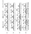
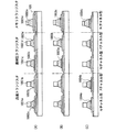
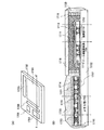
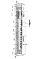
図1〜図3は本発明に係る半導体記憶装置の作製工程を示す図である。
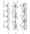
図4は本発明に係る半導体記憶装置の作製工程を示す図である。図4において、図1〜図3と対応する部分については同じ符号を用い、その詳細な説明として実施形態1の説明を参照する。
102 活性層
103 活性層
104 活性層
105 第1絶縁膜
106 第1導電膜
107 膜
107a 膜
108 膜
109 第2絶縁膜
110 第2導電膜
111 レジストマスク
112 レジストマスク
114 上部ゲート電極
115 ゲート電極
116 制御ゲート電極
117 パターン
118 パターン
119 下部ゲート電極
120 浮遊ゲート電極
121 層間絶縁膜
122 配線
128 配線
Claims (16)
- 第1の活性層と、前記第1の活性層上の第1ゲート絶縁膜と、前記第1ゲート絶縁膜上の浮遊ゲート電極と、前記浮遊ゲート電極上の第2ゲート絶縁膜と、前記第2ゲート絶縁膜上の制御ゲート電極とを有する第1のトランジスタと、
第2の活性層と、前記第2の活性層上のゲート絶縁膜と、前記ゲート絶縁膜上のゲート電極を有する第2のトランジスタと、
を同一基板上に有し、
第2のトランジスタの前記ゲート絶縁膜は下部ゲート絶縁膜と上部ゲート絶縁膜を有し、
第2のトランジスタの前記下部ゲート絶縁膜は前記第1ゲート絶縁膜と同じ層から形成され、前記上部ゲート絶縁膜は前記第2ゲート絶縁膜と同じ層から形成されていることを特徴とする半導体装置。 - 第1の活性層と、前記第1の活性層上の第1ゲート絶縁膜と、前記第1ゲート絶縁膜上の浮遊ゲート電極と、前記浮遊ゲート電極上の第2ゲート絶縁膜と、前記第2ゲート絶縁膜上の制御ゲート電極とを有する第1のトランジスタと、
第2の活性層と、前記第2の活性層上のゲート絶縁膜と、前記ゲート絶縁膜上のゲート電極とを有する第2のトランジスタと、
を同一基板上に有し、
第2トランジスタの前記ゲート電極は下部ゲート電極と上部ゲート電極とを有し、
第2のトランジスタの前記下部ゲート電極は前記浮遊ゲート電極と同じ層から形成され、前記上部ゲート電極は前記制御ゲート電極と同じ層から形成されていることを特徴とする半導体装置。 - 第1の活性層と、前記第1の活性層上の第1ゲート絶縁膜と、前記第1ゲート絶縁膜上の浮遊ゲート電極と、前記浮遊ゲート電極上の第2ゲート絶縁膜と、前記第2ゲート絶縁膜上の制御ゲート電極とを有する第1のトランジスタと、
第2の活性層と、前記第2の活性層上のゲート絶縁膜と、前記ゲート絶縁膜上のゲート電極とを有する第2のトランジスタと、
第3の活性層と、前記第3の活性層上のゲート絶縁膜と、前記ゲート絶縁膜上のゲート電極を有する第3のトランジスタと、
を同一基板上に有し、
第3のトランジスタの前記ゲート絶縁膜は下部ゲート絶縁膜と上部ゲート絶縁膜を有し、
第3のトランジスタの前記下部ゲート絶縁膜は前記第1ゲート絶縁膜及び第2のトランジスタの前記ゲート絶縁膜と同じ層から形成され、前記上部ゲート絶縁膜は前記第2ゲート絶縁膜と同じ層から形成されており、
第2のトランジスタの前記ゲート電極は下部ゲート電極と上部ゲート電極を有し、
第2のトランジスタの前記下部ゲート電極は前記浮遊ゲート電極と同じ層から形成され、前記上部ゲート電極は前記制御ゲート電極及び第3のトランジスタの前記ゲート電極と同じ層から形成されていることを特徴とする半導体装置。 - 請求項1または請求項2において、前記第1の活性層及び前記第2の活性層は結晶性半導体膜または微結晶半導体膜であることを特徴とする半導体装置。
- 請求項2または請求項3において、前記制御ゲート電極と同じ層から形成された前記上部ゲート電極を用いて、第2のトランジスタの前記ゲート電極の引き回しがされていることを特徴とする半導体装置。
- 請求項1乃至請求項5のいずれか一項において、前記基板は半導体基板、石英基板、ガラス基板またはプラスチック基板であることを特徴とする半導体装置。
- 請求項1乃至請求項6のいずれか一項において、前記半導体装置は携帯情報端末、ビデオカメラ、デジタルカメラ、パーソナルコンピュータ、テレビ受像器または投影型表示装置であることを特徴とする半導体装置。
- 請求項1乃至請求項6のいずれか一項において、前記半導体装置はIDタグであることを特徴とする半導体装置。
- 第1のトランジスタの活性層と第2のトランジスタの活性層上に第1絶縁膜を形成し、
前記第1絶縁膜上に第1導電膜を形成し、
前記第1導電膜を選択的にエッチングすることにより、前記第2のトランジスタの活性層上の前記第1導電膜を除去して、前記第2のトランジスタの活性層上の前記第1絶縁膜を露出させ、
前記エッチングされた第1導電膜及び前記露出した第1絶縁膜上に第2絶縁膜を形成し、
前記第2絶縁膜上に第2導電膜を形成し、
前記第2導電膜をエッチングすることにより、第2のトランジスタのゲート電極及び第1のトランジスタの制御ゲート電極を形成し、
前記第2導電膜のエッチングの後、前記第2絶縁膜をエッチングし、
前記第2絶縁膜のエッチングの後、前記エッチングされた第1導電膜をエッチングすることにより、第2のトランジスタの浮遊ゲート電極を形成し、
第2のトランジスタのゲート絶縁膜は前記第1絶縁膜及び前記第2絶縁膜からなり、
第1のトランジスタと第2のトランジスタは同一基板上に設けられていることを特徴とする半導体装置の作製方法。 - 第1のトランジスタの活性層と第2のトランジスタの活性層上に第1絶縁膜を形成し、
前記第1絶縁膜上に第1導電膜を形成し、
前記第1導電膜上に第2絶縁膜を形成し、
前記第2絶縁膜を選択的にエッチングすることにより、前記第2のトランジスタの活性層上の前記第2絶縁膜を除去して、前記第2のトランジスタの活性層上の第1導電膜を露出させ、
前記エッチングされた第2絶縁膜及び前記露出された第1導電膜上に、第2導電膜を形成し、
前記第2導電膜をエッチングすることにより、第2のトランジスタの上部ゲート電極と第1のトランジスタの制御ゲート電極を形成し、
前記第1導電膜をエッチングすることにより、第2のトランジスタの下部ゲート電極と第1のトランジスタの浮遊ゲート電極を形成し、
第1のトランジスタと第2のトランジスタは同一基板上に設けられていることを特徴とする半導体装置の作製方法。 - 第1のトランジスタの活性層、第2のトランジスタの活性層及び第3のトランジスタの活性層上に第1絶縁膜を形成し、
前記第1絶縁膜上に第1導電膜を形成し、
前記第1導電膜に選択的に第1のエッチングをすることにより、前記第3のトランジスタの活性層上の前記第1導電膜を除去して、前記第3のトランジスタの活性層上の第1絶縁膜を露出させ、
前記第1のエッチングをされた第1導電膜及び前記露出した第1絶縁膜上に、第2絶縁膜を形成し、
前記第2絶縁膜に選択的に第2のエッチングをすることにより、前記第2のトランジスタの活性層上の前記第2絶縁膜を除去して、前記第2のトランジスタの活性層上の第1導電膜を露出させ、
前記第2のエッチングをされた第2絶縁膜及び前記露出した第1導電膜上に、第2導電膜を形成し、
前記第2導電膜に第3のエッチングをすることにより、第1のトランジスタの制御ゲート電極、第2のトランジスタの上部ゲート電極及び第3のトランジスタのゲート電極及びを形成し、
前記第2のエッチングをされた第2絶縁膜に第4のエッチングをし、
前記第1のエッチングをされた第1導電膜に第5のエッチングをすることにより、第1のトランジスタの浮遊ゲート電極及び第2のトランジスタの下部ゲート電極を形成し、
第3のトランジスタのゲート絶縁膜は前記第1絶縁膜及び前記第2絶縁膜からなり、
第1のトランジスタ、第2のトランジスタ及び第3のトランジスタは同一基板上に設けられることを特徴とする半導体装置の作製方法。 - 請求項11において、前記第1のエッチングにより、前記第1のトランジスタの活性層を覆う前記第1導電膜のパターンと、前記第2トランジスタの活性層を覆う前記第1導電膜のパターンとが形成されることを特徴とする半導体装置の作製方法。
- 請求項11または請求項12において、前記第3乃至第5のエッチングは、それぞれのトランジスタにおいて、同一の一つのレジストマスクを用いて行われることを特徴とする半導体装置の作製方法。
- 請求項9乃至請求項13のいずれか一項において、前記浮遊ゲート電極は窒化タンタル膜またはタンタル膜からなり、前記制御ゲート電極はタングステン膜からなることを特徴とする半導体装置の作製方法。
- 請求項9乃至請求項14のいずれか一項において、前記第1導電膜の膜厚は5〜100nmであることを特徴とする半導体装置の作製方法。
- 請求項9乃至請求項15のいずれか一項において、前記基板は半導体基板、石英基板、ガラス基板またはプラスチック基板であることを特徴とする半導体装置の作製方法。
Priority Applications (1)
| Application Number | Priority Date | Filing Date | Title |
|---|---|---|---|
| JP2005061959A JP4896416B2 (ja) | 2004-03-08 | 2005-03-07 | 半導体装置の作製方法 |
Applications Claiming Priority (3)
| Application Number | Priority Date | Filing Date | Title |
|---|---|---|---|
| JP2004063901 | 2004-03-08 | ||
| JP2004063901 | 2004-03-08 | ||
| JP2005061959A JP4896416B2 (ja) | 2004-03-08 | 2005-03-07 | 半導体装置の作製方法 |
Publications (3)
| Publication Number | Publication Date |
|---|---|
| JP2005294814A true JP2005294814A (ja) | 2005-10-20 |
| JP2005294814A5 JP2005294814A5 (ja) | 2008-03-27 |
| JP4896416B2 JP4896416B2 (ja) | 2012-03-14 |
Family
ID=35327350
Family Applications (1)
| Application Number | Title | Priority Date | Filing Date |
|---|---|---|---|
| JP2005061959A Expired - Fee Related JP4896416B2 (ja) | 2004-03-08 | 2005-03-07 | 半導体装置の作製方法 |
Country Status (1)
| Country | Link |
|---|---|
| JP (1) | JP4896416B2 (ja) |
Cited By (11)
| Publication number | Priority date | Publication date | Assignee | Title |
|---|---|---|---|---|
| WO2007077850A1 (en) * | 2005-12-27 | 2007-07-12 | Semiconductor Energy Laboratory Co., Ltd. | Semiconductor device and manufacturing method thereof |
| JP2007288177A (ja) * | 2006-03-21 | 2007-11-01 | Semiconductor Energy Lab Co Ltd | 不揮発性半導体記憶装置 |
| JP2007288176A (ja) * | 2006-03-21 | 2007-11-01 | Semiconductor Energy Lab Co Ltd | 不揮発性半導体記憶装置 |
| JP2007294911A (ja) * | 2006-03-31 | 2007-11-08 | Semiconductor Energy Lab Co Ltd | 不揮発性半導体記憶装置 |
| JP2007294910A (ja) * | 2006-03-31 | 2007-11-08 | Semiconductor Energy Lab Co Ltd | 不揮発性半導体記憶装置 |
| WO2007138754A1 (ja) * | 2006-05-31 | 2007-12-06 | Sharp Kabushiki Kaisha | 半導体装置、その製造方法、及び、表示装置 |
| JP2007324561A (ja) * | 2006-06-02 | 2007-12-13 | Hynix Semiconductor Inc | 集積回路及び該情報記録方法 |
| US7745827B2 (en) | 2005-09-29 | 2010-06-29 | Semiconductor Energy Laboratory Co., Ltd. | Memory device |
| JP2013051425A (ja) * | 2006-03-31 | 2013-03-14 | Semiconductor Energy Lab Co Ltd | 半導体装置 |
| US8581260B2 (en) | 2007-02-22 | 2013-11-12 | Semiconductor Energy Laboratory Co., Ltd. | Semiconductor device including a memory |
| KR101345418B1 (ko) * | 2006-03-21 | 2013-12-24 | 가부시키가이샤 한도오따이 에네루기 켄큐쇼 | 불휘발성 반도체 기억장치 |
Citations (4)
| Publication number | Priority date | Publication date | Assignee | Title |
|---|---|---|---|---|
| JPH09148458A (ja) * | 1995-11-08 | 1997-06-06 | Lg Semicon Co Ltd | 浮遊ゲートを有する半導体素子の製造方法 |
| JPH1187545A (ja) * | 1997-07-08 | 1999-03-30 | Sony Corp | 半導体不揮発性記憶装置およびその製造方法 |
| JP2003518742A (ja) * | 1999-12-21 | 2003-06-10 | コーニンクレッカ フィリップス エレクトロニクス エヌ ヴィ | 不揮発性のメモリーセルと周辺部 |
| JP2003249579A (ja) * | 2003-02-10 | 2003-09-05 | Toshiba Corp | 不揮発性半導体記憶装置およびその製造方法 |
-
2005
- 2005-03-07 JP JP2005061959A patent/JP4896416B2/ja not_active Expired - Fee Related
Patent Citations (4)
| Publication number | Priority date | Publication date | Assignee | Title |
|---|---|---|---|---|
| JPH09148458A (ja) * | 1995-11-08 | 1997-06-06 | Lg Semicon Co Ltd | 浮遊ゲートを有する半導体素子の製造方法 |
| JPH1187545A (ja) * | 1997-07-08 | 1999-03-30 | Sony Corp | 半導体不揮発性記憶装置およびその製造方法 |
| JP2003518742A (ja) * | 1999-12-21 | 2003-06-10 | コーニンクレッカ フィリップス エレクトロニクス エヌ ヴィ | 不揮発性のメモリーセルと周辺部 |
| JP2003249579A (ja) * | 2003-02-10 | 2003-09-05 | Toshiba Corp | 不揮発性半導体記憶装置およびその製造方法 |
Cited By (19)
| Publication number | Priority date | Publication date | Assignee | Title |
|---|---|---|---|---|
| US7745827B2 (en) | 2005-09-29 | 2010-06-29 | Semiconductor Energy Laboratory Co., Ltd. | Memory device |
| US8476632B2 (en) | 2005-12-27 | 2013-07-02 | Semiconductor Energy Laboratory Co., Ltd. | Semiconductor device and manufacturing method thereof |
| WO2007077850A1 (en) * | 2005-12-27 | 2007-07-12 | Semiconductor Energy Laboratory Co., Ltd. | Semiconductor device and manufacturing method thereof |
| US9177242B2 (en) | 2005-12-27 | 2015-11-03 | Semiconductor Energy Laboratory Co., Ltd. | Semiconductor device and manufacturing method thereof |
| EP1966740A4 (en) * | 2005-12-27 | 2014-08-27 | Semiconductor Energy Lab | SEMICONDUCTOR COMPONENT AND MANUFACTURING METHOD THEREFOR |
| JP2010056566A (ja) * | 2005-12-27 | 2010-03-11 | Semiconductor Energy Lab Co Ltd | 半導体装置及び表示機能付きicカード |
| JP2007200291A (ja) * | 2005-12-27 | 2007-08-09 | Semiconductor Energy Lab Co Ltd | 半導体装置およびその作製方法 |
| KR101233639B1 (ko) | 2005-12-27 | 2013-02-15 | 가부시키가이샤 한도오따이 에네루기 켄큐쇼 | 반도체장치 및 그 제조방법 |
| JP2007288176A (ja) * | 2006-03-21 | 2007-11-01 | Semiconductor Energy Lab Co Ltd | 不揮発性半導体記憶装置 |
| US8729620B2 (en) | 2006-03-21 | 2014-05-20 | Semiconductor Energy Laboratory Co., Ltd. | Nonvolatile semiconductor memory device |
| KR101345418B1 (ko) * | 2006-03-21 | 2013-12-24 | 가부시키가이샤 한도오따이 에네루기 켄큐쇼 | 불휘발성 반도체 기억장치 |
| JP2007288177A (ja) * | 2006-03-21 | 2007-11-01 | Semiconductor Energy Lab Co Ltd | 不揮発性半導体記憶装置 |
| JP2013051425A (ja) * | 2006-03-31 | 2013-03-14 | Semiconductor Energy Lab Co Ltd | 半導体装置 |
| US8629490B2 (en) | 2006-03-31 | 2014-01-14 | Semiconductor Energy Laboratory Co., Ltd. | Nonvolatile semiconductor storage device with floating gate electrode and control gate electrode |
| JP2007294910A (ja) * | 2006-03-31 | 2007-11-08 | Semiconductor Energy Lab Co Ltd | 不揮発性半導体記憶装置 |
| JP2007294911A (ja) * | 2006-03-31 | 2007-11-08 | Semiconductor Energy Lab Co Ltd | 不揮発性半導体記憶装置 |
| WO2007138754A1 (ja) * | 2006-05-31 | 2007-12-06 | Sharp Kabushiki Kaisha | 半導体装置、その製造方法、及び、表示装置 |
| JP2007324561A (ja) * | 2006-06-02 | 2007-12-13 | Hynix Semiconductor Inc | 集積回路及び該情報記録方法 |
| US8581260B2 (en) | 2007-02-22 | 2013-11-12 | Semiconductor Energy Laboratory Co., Ltd. | Semiconductor device including a memory |
Also Published As
| Publication number | Publication date |
|---|---|
| JP4896416B2 (ja) | 2012-03-14 |
Similar Documents
| Publication | Publication Date | Title |
|---|---|---|
| CN1691337B (zh) | 半导体装置及其制造方法 | |
| US10896931B1 (en) | 3D semiconductor device and structure | |
| US7972935B2 (en) | Method for manufacturing semiconductor device | |
| JP5604492B2 (ja) | 半導体装置 | |
| US7846817B2 (en) | Method for manufacturing semiconductor device | |
| JP4896416B2 (ja) | 半導体装置の作製方法 | |
| KR20030078075A (ko) | 초박형 수직 바디 트랜지스터를 갖는 프로그래밍 가능한메모리 어드레스 및 디코드 회로 | |
| US20180331073A1 (en) | 3d semiconductor device and structure | |
| US8569170B2 (en) | Manufacturing method of semiconductor device comprising silicide layer with varied thickness | |
| US11462586B1 (en) | Method to produce 3D semiconductor devices and structures with memory | |
| KR101781482B1 (ko) | 안티퓨즈 소자, 이를 포함하는 반도체 장치 및 시스템 | |
| US12015026B2 (en) | Methods of forming circuit-protection devices | |
| US20060197088A1 (en) | Semiconductor device and manufacturing method of the same | |
| JP4839904B2 (ja) | 半導体装置、集積回路、及び電子機器 | |
| US10290682B2 (en) | 3D IC semiconductor device and structure with stacked memory | |
| CN1832176B (zh) | 半导体器件及其操作方法 | |
| US11257867B1 (en) | 3D semiconductor device and structure with oxide bonds | |
| JP2013239516A (ja) | 半導体装置およびその製造方法 | |
| JP2007250862A (ja) | 半導体装置、集積回路、及び電子機器 | |
| US11469271B2 (en) | Method to produce 3D semiconductor devices and structures with memory | |
| US10825864B2 (en) | 3D semiconductor device and structure | |
| JP2007294915A (ja) | 不揮発性半導体記憶装置及びその作製方法 | |
| JP2008177327A (ja) | 半導体装置およびその製造方法 |
Legal Events
| Date | Code | Title | Description |
|---|---|---|---|
| A521 | Request for written amendment filed |
Free format text: JAPANESE INTERMEDIATE CODE: A523 Effective date: 20080212 |
|
| A621 | Written request for application examination |
Free format text: JAPANESE INTERMEDIATE CODE: A621 Effective date: 20080212 |
|
| A977 | Report on retrieval |
Free format text: JAPANESE INTERMEDIATE CODE: A971007 Effective date: 20100831 |
|
| A131 | Notification of reasons for refusal |
Free format text: JAPANESE INTERMEDIATE CODE: A131 Effective date: 20110913 |
|
| A521 | Request for written amendment filed |
Free format text: JAPANESE INTERMEDIATE CODE: A523 Effective date: 20111020 |
|
| TRDD | Decision of grant or rejection written | ||
| A01 | Written decision to grant a patent or to grant a registration (utility model) |
Free format text: JAPANESE INTERMEDIATE CODE: A01 Effective date: 20111220 |
|
| A01 | Written decision to grant a patent or to grant a registration (utility model) |
Free format text: JAPANESE INTERMEDIATE CODE: A01 |
|
| A61 | First payment of annual fees (during grant procedure) |
Free format text: JAPANESE INTERMEDIATE CODE: A61 Effective date: 20111221 |
|
| R150 | Certificate of patent or registration of utility model |
Free format text: JAPANESE INTERMEDIATE CODE: R150 |
|
| FPAY | Renewal fee payment (event date is renewal date of database) |
Free format text: PAYMENT UNTIL: 20150106 Year of fee payment: 3 |
|
| FPAY | Renewal fee payment (event date is renewal date of database) |
Free format text: PAYMENT UNTIL: 20150106 Year of fee payment: 3 |
|
| R250 | Receipt of annual fees |
Free format text: JAPANESE INTERMEDIATE CODE: R250 |
|
| R250 | Receipt of annual fees |
Free format text: JAPANESE INTERMEDIATE CODE: R250 |
|
| R250 | Receipt of annual fees |
Free format text: JAPANESE INTERMEDIATE CODE: R250 |
|
| LAPS | Cancellation because of no payment of annual fees |