JP2005294814A - Semiconductor device and manufacturing method therefor - Google Patents
Semiconductor device and manufacturing method therefor Download PDFInfo
- Publication number
- JP2005294814A JP2005294814A JP2005061959A JP2005061959A JP2005294814A JP 2005294814 A JP2005294814 A JP 2005294814A JP 2005061959 A JP2005061959 A JP 2005061959A JP 2005061959 A JP2005061959 A JP 2005061959A JP 2005294814 A JP2005294814 A JP 2005294814A
- Authority
- JP
- Japan
- Prior art keywords
- transistor
- insulating film
- gate electrode
- film
- active layer
- Prior art date
- Legal status (The legal status is an assumption and is not a legal conclusion. Google has not performed a legal analysis and makes no representation as to the accuracy of the status listed.)
- Granted
Links
- 239000004065 semiconductor Substances 0.000 title claims abstract description 167
- 238000004519 manufacturing process Methods 0.000 title claims abstract description 52
- 239000000758 substrate Substances 0.000 claims abstract description 104
- 238000000034 method Methods 0.000 claims abstract description 61
- 238000005530 etching Methods 0.000 claims description 77
- 238000007667 floating Methods 0.000 claims description 60
- VYPSYNLAJGMNEJ-UHFFFAOYSA-N silicon dioxide Inorganic materials O=[Si]=O VYPSYNLAJGMNEJ-UHFFFAOYSA-N 0.000 claims description 34
- 229910052715 tantalum Inorganic materials 0.000 claims description 13
- GUVRBAGPIYLISA-UHFFFAOYSA-N tantalum atom Chemical compound [Ta] GUVRBAGPIYLISA-UHFFFAOYSA-N 0.000 claims description 13
- MZLGASXMSKOWSE-UHFFFAOYSA-N tantalum nitride Chemical compound [Ta]#N MZLGASXMSKOWSE-UHFFFAOYSA-N 0.000 claims description 13
- 239000011521 glass Substances 0.000 claims description 6
- WFKWXMTUELFFGS-UHFFFAOYSA-N tungsten Chemical compound [W] WFKWXMTUELFFGS-UHFFFAOYSA-N 0.000 claims description 6
- 229910052721 tungsten Inorganic materials 0.000 claims description 6
- 239000010937 tungsten Substances 0.000 claims description 6
- 239000010453 quartz Substances 0.000 claims description 4
- 238000009413 insulation Methods 0.000 claims 1
- 230000015654 memory Effects 0.000 abstract description 99
- 230000008569 process Effects 0.000 abstract description 23
- 230000015572 biosynthetic process Effects 0.000 abstract description 19
- 239000010408 film Substances 0.000 description 445
- 239000010410 layer Substances 0.000 description 90
- 239000012535 impurity Substances 0.000 description 72
- 230000015556 catabolic process Effects 0.000 description 30
- 229910052814 silicon oxide Inorganic materials 0.000 description 30
- 239000000463 material Substances 0.000 description 25
- 108091006146 Channels Proteins 0.000 description 22
- 238000001039 wet etching Methods 0.000 description 14
- 230000006870 function Effects 0.000 description 11
- 239000007789 gas Substances 0.000 description 10
- 239000011229 interlayer Substances 0.000 description 10
- ZOXJGFHDIHLPTG-UHFFFAOYSA-N Boron Chemical compound [B] ZOXJGFHDIHLPTG-UHFFFAOYSA-N 0.000 description 9
- 229910052581 Si3N4 Inorganic materials 0.000 description 9
- 229910052796 boron Inorganic materials 0.000 description 9
- HQVNEWCFYHHQES-UHFFFAOYSA-N silicon nitride Chemical compound N12[Si]34N5[Si]62N3[Si]51N64 HQVNEWCFYHHQES-UHFFFAOYSA-N 0.000 description 9
- OAICVXFJPJFONN-UHFFFAOYSA-N Phosphorus Chemical compound [P] OAICVXFJPJFONN-UHFFFAOYSA-N 0.000 description 7
- 238000010586 diagram Methods 0.000 description 7
- 229910052698 phosphorus Inorganic materials 0.000 description 7
- 239000011574 phosphorus Substances 0.000 description 7
- 230000000694 effects Effects 0.000 description 6
- 239000007772 electrode material Substances 0.000 description 6
- 238000010438 heat treatment Methods 0.000 description 6
- PCHJSUWPFVWCPO-UHFFFAOYSA-N gold Chemical compound [Au] PCHJSUWPFVWCPO-UHFFFAOYSA-N 0.000 description 5
- KRHYYFGTRYWZRS-UHFFFAOYSA-N Fluorane Chemical compound F KRHYYFGTRYWZRS-UHFFFAOYSA-N 0.000 description 4
- XUIMIQQOPSSXEZ-UHFFFAOYSA-N Silicon Chemical compound [Si] XUIMIQQOPSSXEZ-UHFFFAOYSA-N 0.000 description 4
- 230000007547 defect Effects 0.000 description 4
- 229920005989 resin Polymers 0.000 description 4
- 239000011347 resin Substances 0.000 description 4
- 229910052710 silicon Inorganic materials 0.000 description 4
- 239000010703 silicon Substances 0.000 description 4
- 229910052785 arsenic Inorganic materials 0.000 description 3
- RQNWIZPPADIBDY-UHFFFAOYSA-N arsenic atom Chemical compound [As] RQNWIZPPADIBDY-UHFFFAOYSA-N 0.000 description 3
- 238000002347 injection Methods 0.000 description 3
- 239000007924 injection Substances 0.000 description 3
- 238000002955 isolation Methods 0.000 description 3
- 239000010409 thin film Substances 0.000 description 3
- RYGMFSIKBFXOCR-UHFFFAOYSA-N Copper Chemical compound [Cu] RYGMFSIKBFXOCR-UHFFFAOYSA-N 0.000 description 2
- UFHFLCQGNIYNRP-UHFFFAOYSA-N Hydrogen Chemical compound [H][H] UFHFLCQGNIYNRP-UHFFFAOYSA-N 0.000 description 2
- 229910004298 SiO 2 Inorganic materials 0.000 description 2
- 230000001133 acceleration Effects 0.000 description 2
- 229910052782 aluminium Inorganic materials 0.000 description 2
- XAGFODPZIPBFFR-UHFFFAOYSA-N aluminium Chemical compound [Al] XAGFODPZIPBFFR-UHFFFAOYSA-N 0.000 description 2
- 238000000137 annealing Methods 0.000 description 2
- 230000008901 benefit Effects 0.000 description 2
- 229910052802 copper Inorganic materials 0.000 description 2
- 239000010949 copper Substances 0.000 description 2
- 238000001312 dry etching Methods 0.000 description 2
- 229910052739 hydrogen Inorganic materials 0.000 description 2
- 239000001257 hydrogen Substances 0.000 description 2
- 238000009616 inductively coupled plasma Methods 0.000 description 2
- 239000012212 insulator Substances 0.000 description 2
- 238000005468 ion implantation Methods 0.000 description 2
- 238000005224 laser annealing Methods 0.000 description 2
- 238000005499 laser crystallization Methods 0.000 description 2
- 239000004973 liquid crystal related substance Substances 0.000 description 2
- 239000011159 matrix material Substances 0.000 description 2
- 229910052751 metal Inorganic materials 0.000 description 2
- 239000002184 metal Substances 0.000 description 2
- 230000003647 oxidation Effects 0.000 description 2
- 238000007254 oxidation reaction Methods 0.000 description 2
- 230000002093 peripheral effect Effects 0.000 description 2
- 239000011241 protective layer Substances 0.000 description 2
- 229910000679 solder Inorganic materials 0.000 description 2
- 238000003860 storage Methods 0.000 description 2
- JBRZTFJDHDCESZ-UHFFFAOYSA-N AsGa Chemical compound [As]#[Ga] JBRZTFJDHDCESZ-UHFFFAOYSA-N 0.000 description 1
- 229910001218 Gallium arsenide Inorganic materials 0.000 description 1
- 108010075750 P-Type Calcium Channels Proteins 0.000 description 1
- BLRPTPMANUNPDV-UHFFFAOYSA-N Silane Chemical compound [SiH4] BLRPTPMANUNPDV-UHFFFAOYSA-N 0.000 description 1
- 229910000577 Silicon-germanium Inorganic materials 0.000 description 1
- LEVVHYCKPQWKOP-UHFFFAOYSA-N [Si].[Ge] Chemical compound [Si].[Ge] LEVVHYCKPQWKOP-UHFFFAOYSA-N 0.000 description 1
- 229910045601 alloy Inorganic materials 0.000 description 1
- 239000000956 alloy Substances 0.000 description 1
- 230000009286 beneficial effect Effects 0.000 description 1
- 230000001413 cellular effect Effects 0.000 description 1
- 239000000919 ceramic Substances 0.000 description 1
- 230000008859 change Effects 0.000 description 1
- 150000001875 compounds Chemical class 0.000 description 1
- 229910021419 crystalline silicon Inorganic materials 0.000 description 1
- ZOCHARZZJNPSEU-UHFFFAOYSA-N diboron Chemical compound B#B ZOCHARZZJNPSEU-UHFFFAOYSA-N 0.000 description 1
- 238000000113 differential scanning calorimetry Methods 0.000 description 1
- 238000005516 engineering process Methods 0.000 description 1
- 230000001747 exhibiting effect Effects 0.000 description 1
- 239000000284 extract Substances 0.000 description 1
- 239000000945 filler Substances 0.000 description 1
- 229910052732 germanium Inorganic materials 0.000 description 1
- GNPVGFCGXDBREM-UHFFFAOYSA-N germanium atom Chemical compound [Ge] GNPVGFCGXDBREM-UHFFFAOYSA-N 0.000 description 1
- 238000005984 hydrogenation reaction Methods 0.000 description 1
- 238000002513 implantation Methods 0.000 description 1
- 150000002500 ions Chemical class 0.000 description 1
- 230000014759 maintenance of location Effects 0.000 description 1
- 239000012528 membrane Substances 0.000 description 1
- 239000000203 mixture Substances 0.000 description 1
- 229910021421 monocrystalline silicon Inorganic materials 0.000 description 1
- 239000002105 nanoparticle Substances 0.000 description 1
- 238000004806 packaging method and process Methods 0.000 description 1
- 238000002161 passivation Methods 0.000 description 1
- 238000005268 plasma chemical vapour deposition Methods 0.000 description 1
- 238000001020 plasma etching Methods 0.000 description 1
- 229920001690 polydopamine Polymers 0.000 description 1
- 238000007639 printing Methods 0.000 description 1
- 239000002994 raw material Substances 0.000 description 1
- 230000009467 reduction Effects 0.000 description 1
- 238000007650 screen-printing Methods 0.000 description 1
- 238000004904 shortening Methods 0.000 description 1
- 229910000077 silane Inorganic materials 0.000 description 1
- 229910010271 silicon carbide Inorganic materials 0.000 description 1
- HBMJWWWQQXIZIP-UHFFFAOYSA-N silicon carbide Chemical compound [Si+]#[C-] HBMJWWWQQXIZIP-UHFFFAOYSA-N 0.000 description 1
- 239000002356 single layer Substances 0.000 description 1
- 238000005549 size reduction Methods 0.000 description 1
- 239000007790 solid phase Substances 0.000 description 1
- 238000004544 sputter deposition Methods 0.000 description 1
- 239000010935 stainless steel Substances 0.000 description 1
- 229910001220 stainless steel Inorganic materials 0.000 description 1
- 229920003002 synthetic resin Polymers 0.000 description 1
- 239000000057 synthetic resin Substances 0.000 description 1
- 238000002230 thermal chemical vapour deposition Methods 0.000 description 1
- 230000007704 transition Effects 0.000 description 1
Images

Landscapes
- Semiconductor Memories (AREA)
- Non-Volatile Memory (AREA)
Abstract
Description
本発明は、基板上にメモリトランジスタを有する半導体装置及びその作製方法に関するものである。 The present invention relates to a semiconductor device having a memory transistor on a substrate and a manufacturing method thereof.
近年、データやプログラムを記憶する不揮発性の半導体記憶素子を持つコンピュータ等の半導体記憶装置が増えている。半導体記憶装置は一般的に、データが記憶されるメモリトランジスタ(メモリセルトランジスタとも言う)を複数有するメモリセルアレイと、書込み、消去、または読み出しを行う回路と、アドレス信号によりメモリトランジスタの場所を特定するデコーダとで構成される。これら各回路を構成する素子は、それぞれに求められる特性が異なるため、これに伴いその構成も異なる。 In recent years, semiconductor memory devices such as computers having nonvolatile semiconductor memory elements for storing data and programs are increasing. A semiconductor memory device generally specifies a memory cell array having a plurality of memory transistors (also referred to as memory cell transistors) in which data is stored, a circuit that performs writing, erasing, or reading, and a memory transistor location by an address signal It consists of a decoder. Since the elements constituting each of these circuits have different required characteristics, the configurations thereof are different accordingly.
半導体不揮発性メモリを代表するメモリとして、EEPROM(Electric Erasable Programmable Read Only Memory)やフラッシュメモリ(flash memory)が知られている。これらのようなメモリのうち、浮遊ゲート電極を有するメモリトランジスタを用いる場合は、メモリトランジスタの半導体層と浮遊ゲート電極との間にあるトンネル酸化膜をできるだけ薄くする必要がある。なぜなら、トンネル酸化膜はトンネル電流が流れる程度の薄さでなければならないからである。また、浮遊ゲート電極やトンネル酸化膜の他に、制御ゲート電極と、制御ゲート電極と浮遊ゲート電極とに挟まれる絶縁膜を有するため、メモリトランジスタは2つのゲート電極と2つの絶縁膜で構成されている。 As a representative memory of a semiconductor nonvolatile memory, an EEPROM (Electrically Erasable Programmable Read Only Memory) and a flash memory (flash memory) are known. Of these memories, when using a memory transistor having a floating gate electrode, it is necessary to make the tunnel oxide film between the semiconductor layer of the memory transistor and the floating gate electrode as thin as possible. This is because the tunnel oxide film must be thin enough to allow a tunnel current to flow. In addition to the floating gate electrode and the tunnel oxide film, the memory transistor includes two gate electrodes and two insulating films because the control gate electrode and an insulating film sandwiched between the control gate electrode and the floating gate electrode are included. ing.
デコーダを構成するトランジスタは、高速動作が必要とされるため、ゲート絶縁膜が薄膜であるのが望ましい。 Since the transistor constituting the decoder is required to operate at high speed, the gate insulating film is preferably a thin film.
一方で、書込みや消去、読み出しを行う回路では、その動作上、回路を構成するトランジスタに、メモリトランジスタにかかる電圧と同程度の高電圧がかかるため、そのような状況でもトランジスタが破壊されないよう、ゲート絶縁膜を厚くする必要がある。 On the other hand, in a circuit that performs writing, erasing, and reading, a transistor that constitutes the circuit is applied with a high voltage that is about the same as the voltage applied to the memory transistor, so that the transistor is not destroyed even in such a situation. It is necessary to increase the thickness of the gate insulating film.
以上のように、半導体記憶装置は構成の異なる素子を集積して作製されている。 As described above, the semiconductor memory device is manufactured by integrating elements having different configurations.
関連技術として、同一基板上に画素部、駆動回路部、メモリ部を一体形成したアクティブマトリクス基板を作製する技術があり、この場合にも、アクティブマトリクス基板上に、構成の異なるトランジスタが集積化されて作製されている。具体的には、各機能に応じた構造のトランジスタを作製するため、メモリ部のトランジスタのゲート絶縁膜を、画素部や駆動回路部のゲート絶縁膜の膜厚よりも薄くしている。(以上、特許文献1参照)。
上述した構成の異なるトランジスタを集積化して半導体記憶装置を同一基板上に作製する場合、ゲート絶縁膜が厚い素子や薄い素子、ゲート電極が1つの素子や2つの素子等が混在するため、自然と工程数が多くなる傾向があった。また、構成の異なる素子を各々作製してから配線で互いに接続すれば工程数は短縮されるが、半導体記憶装置が大型化してしまうという問題があった。 When a semiconductor memory device is manufactured on the same substrate by integrating transistors having different structures as described above, a device having a thick gate insulating film or a thin device, a device having one gate electrode or two devices, etc. are mixed. There was a tendency for the number of processes to increase. Further, if elements having different configurations are manufactured and then connected to each other by wiring, the number of steps can be reduced, but there is a problem that the semiconductor memory device is increased in size.
そこで本発明は、工程数を短縮しつつ、同一基板上に構成の異なる素子を作り込んだ半導体装置及びその作製プロセスを提供することを目的とする。 Accordingly, an object of the present invention is to provide a semiconductor device in which elements having different configurations are formed over the same substrate and the manufacturing process thereof while reducing the number of steps.
上記課題を解決するために、本発明の半導体装置は、第1の活性層と、第1の活性層上の第1ゲート絶縁膜と、第1ゲート絶縁膜上の浮遊ゲート電極と、浮遊ゲート電極上の第2ゲート絶縁膜と、第2ゲート絶縁膜上の制御ゲート電極とを有する第1のトランジスタとを有し、また、第2の活性層と、第2の活性層上のゲート絶縁膜と、ゲート絶縁膜上のゲート電極を有する第2のトランジスタとを有し、これら第1のトランジスタと第2のトランジスタを同一基板上に設け、第2のトランジスタのゲート絶縁膜は下部ゲート絶縁膜と上部ゲート絶縁膜を有しており、第2のトランジスタの下部ゲート絶縁膜は第1ゲート絶縁膜と同じ層から形成され、上部ゲート絶縁膜は第2ゲート絶縁膜と同じ層から形成されていることを特徴とするものである。 In order to solve the above problems, a semiconductor device of the present invention includes a first active layer, a first gate insulating film on the first active layer, a floating gate electrode on the first gate insulating film, and a floating gate. A first transistor having a second gate insulating film on the electrode and a control gate electrode on the second gate insulating film; and a second active layer and a gate insulating on the second active layer And a second transistor having a gate electrode on the gate insulating film, the first transistor and the second transistor are provided on the same substrate, and the gate insulating film of the second transistor is a lower gate insulating film. And a lower gate insulating film of the second transistor is formed from the same layer as the first gate insulating film, and the upper gate insulating film is formed from the same layer as the second gate insulating film. It is characterized by having A.
また、本発明の半導体装置は、第1の活性層と、第1の活性層上の第1ゲート絶縁膜と、第1ゲート絶縁膜上の浮遊ゲート電極と、浮遊ゲート電極上の第2ゲート絶縁膜と、第2ゲート絶縁膜上の制御ゲート電極とを有する第1のトランジスタと、第2の活性層と、第2の活性層上のゲート絶縁膜と、ゲート絶縁膜上のゲート電極とを有する第2のトランジスタとを有し、これら第1のトランジスタと第2のトランジスタを同一基板上に設け、第2トランジスタのゲート電極は下部ゲート電極と上部ゲート電極とを有しており、第2のトランジスタの下部ゲート電極は浮遊ゲート電極と同じ層から形成され、上部ゲート電極は制御ゲート電極と同じ層から形成されていることを特徴とするものである。
The semiconductor device of the present invention includes a first active layer, a first gate insulating film on the first active layer, a floating gate electrode on the first gate insulating film, and a second gate on the floating gate electrode. A first transistor having an insulating film and a control gate electrode on the second gate insulating film; a second active layer; a gate insulating film on the second active layer; and a gate electrode on the gate insulating film; The first transistor and the second transistor are provided on the same substrate, and the gate electrode of the second transistor has a lower gate electrode and an upper gate electrode, The lower gate electrode of the
また、第1の活性層と、第1の活性層上の第1ゲート絶縁膜と、第1ゲート絶縁膜上の浮遊ゲート電極と、浮遊ゲート電極上の第2ゲート絶縁膜と、第2ゲート絶縁膜上の制御ゲート電極とを有する第1のトランジスタと、第2の活性層と、第2の活性層上のゲート絶縁膜と、ゲート絶縁膜上のゲート電極とを有する第2のトランジスタと、第3の活性層と、第3の活性層上のゲート絶縁膜と、ゲート絶縁膜上のゲート電極を有する第3のトランジスタとを有しており、これら第1乃至第3のトランジスタを同一基板上に設け、第3のトランジスタのゲート絶縁膜は下部ゲート絶縁膜と上部ゲート絶縁膜を有し、第3のトランジスタの下部ゲート絶縁膜は第1ゲート絶縁膜及び第2のトランジスタのゲート絶縁膜と同じ層から形成され、上部ゲート絶縁膜は第2ゲート絶縁膜と同じ層から形成されており、第2のトランジスタのゲート電極は下部ゲート電極と上部ゲート電極を有し、第2のトランジスタの下部ゲート電極は浮遊ゲート電極と同じ層から形成され、上部ゲート電極は制御ゲート電極及び第3のトランジスタのゲート電極と同じ層から形成されていることを特徴とするものである。 Also, the first active layer, the first gate insulating film on the first active layer, the floating gate electrode on the first gate insulating film, the second gate insulating film on the floating gate electrode, and the second gate A first transistor having a control gate electrode on an insulating film; a second active layer; a second transistor having a gate insulating film on the second active layer; and a gate electrode on the gate insulating film; , A third active layer, a gate insulating film on the third active layer, and a third transistor having a gate electrode on the gate insulating film, and the first to third transistors are the same. Provided on the substrate, the gate insulating film of the third transistor has a lower gate insulating film and an upper gate insulating film, and the lower gate insulating film of the third transistor is a gate insulating film of the first gate insulating film and the second transistor. Formed from the same layer as the membrane, the top The gate insulating film is formed from the same layer as the second gate insulating film, the gate electrode of the second transistor has a lower gate electrode and an upper gate electrode, and the lower gate electrode of the second transistor is a floating gate electrode The upper gate electrode is formed from the same layer as the control gate electrode and the gate electrode of the third transistor.
第1のトランジスタの制御ゲート電極と同じ層から形成された上部ゲート電極を用いて、第2のトランジスタのゲート電極の引き回しがされていることを特徴とするものである。 The gate electrode of the second transistor is routed using the upper gate electrode formed from the same layer as the control gate electrode of the first transistor.
活性層は結晶性半導体膜または微結晶半導体膜であることを特徴とするものである。 The active layer is a crystalline semiconductor film or a microcrystalline semiconductor film.
本発明の半導体装置は、第1のトランジスタの活性層と第2のトランジスタの活性層上に第1絶縁膜を形成し、第1絶縁膜上に第1導電膜を形成し、第1導電膜を選択的にエッチングすることにより、第2のトランジスタの活性層上の第1導電膜を除去して、第2のトランジスタの活性層上の第1絶縁膜を露出させ、エッチングされた第1導電膜及び露出した第1絶縁膜上に第2絶縁膜を形成し、第2絶縁膜上に第2導電膜を形成し、第2導電膜をエッチングすることにより、第2のトランジスタのゲート電極及び第1のトランジスタの制御ゲート電極を形成し、第2導電膜のエッチングの後、第2絶縁膜をエッチングし、第2絶縁膜のエッチングの後、エッチングされた第1導電膜をエッチングすることにより、第2のトランジスタの浮遊ゲート電極を形成し、第2のトランジスタのゲート絶縁膜は第1絶縁膜及び第2絶縁膜からなり、第1のトランジスタと第2のトランジスタは同一基板上に設けられていることを特徴とするものである。 In the semiconductor device of the present invention, a first insulating film is formed on the active layer of the first transistor and the active layer of the second transistor, a first conductive film is formed on the first insulating film, and the first conductive film is formed. Is selectively etched to remove the first conductive film on the active layer of the second transistor, to expose the first insulating film on the active layer of the second transistor, and to etch the first conductive film. Forming a second insulating film on the film and the exposed first insulating film, forming a second conductive film on the second insulating film, and etching the second conductive film; By forming a control gate electrode of the first transistor, etching the second conductive film, etching the second insulating film, etching the second insulating film, and then etching the etched first conductive film The floating of the second transistor A gate electrode of the second transistor is composed of a first insulating film and a second insulating film, and the first transistor and the second transistor are provided on the same substrate. To do.
本発明の半導体装置は、第1のトランジスタの活性層と第2のトランジスタの活性層上に第1絶縁膜を形成し、第1絶縁膜上に第1導電膜を形成し、第1導電膜上に第2絶縁膜を形成し、第2絶縁膜を選択的にエッチングすることにより、第2のトランジスタの活性層上の第2絶縁膜を除去して、第2のトランジスタの活性層上の第1導電膜を露出させ、エッチングされた第2絶縁膜及び露出された第1導電膜上に、第2導電膜を形成し、第2導電膜をエッチングすることにより、第2のトランジスタの上部ゲート電極と第1のトランジスタの制御ゲート電極を形成し、第1導電膜をエッチングすることにより、第2のトランジスタの下部ゲート電極と第1のトランジスタの浮遊ゲート電極を形成し、第1のトランジスタと第2のトランジスタは同一基板上に設けられていることを特徴とするものである。 In the semiconductor device of the present invention, a first insulating film is formed on the active layer of the first transistor and the active layer of the second transistor, a first conductive film is formed on the first insulating film, and the first conductive film is formed. A second insulating film is formed thereon, and the second insulating film is selectively etched to remove the second insulating film on the active layer of the second transistor, and on the active layer of the second transistor. An upper portion of the second transistor is formed by exposing the first conductive film, forming a second conductive film on the etched second insulating film and the exposed first conductive film, and etching the second conductive film. A gate electrode and a control gate electrode of the first transistor are formed, and the first conductive film is etched to form a lower gate electrode of the second transistor and a floating gate electrode of the first transistor. And the second transition It is characterized in that provided on the same substrate.
本発明の半導体装置は、第1のトランジスタの活性層、第2のトランジスタの活性層及び第3のトランジスタの活性層上に第1絶縁膜を形成し、第1絶縁膜上に第1導電膜を形成し、第1導電膜に選択的に第1のエッチングをすることにより、第3のトランジスタの活性層上の第1導電膜を除去して、第3のトランジスタの活性層上の第1絶縁膜を露出させ、第1のエッチングをされた第1導電膜及び露出した第1絶縁膜上に、第2絶縁膜を形成し、第2絶縁膜に選択的に第2のエッチングをすることにより、第2のトランジスタの活性層上の第2絶縁膜を除去して、第2のトランジスタの活性層上の第1導電膜を露出させ、第2のエッチングをされた第2絶縁膜及び露出した第1導電膜上に、第2導電膜を形成し、第2導電膜に第3のエッチングをすることにより、第1のトランジスタの制御ゲート電極、第2のトランジスタの上部ゲート電極及び第3のトランジスタのゲート電極を形成し、第2のエッチングをされた第2絶縁膜に第4のエッチングをし、第1のエッチングをされた第1導電膜に第5のエッチングをすることにより、第1のトランジスタの浮遊ゲート電極及び第2のトランジスタの下部ゲート電極を形成し、第3のトランジスタのゲート絶縁膜は第1絶縁膜及び第2絶縁膜からなり、第1のトランジスタ、第2のトランジスタ及び第3のトランジスタは同一基板上に設けられることを特徴とするものである。 In the semiconductor device of the present invention, a first insulating film is formed on the active layer of the first transistor, the active layer of the second transistor, and the active layer of the third transistor, and the first conductive film is formed on the first insulating film. The first conductive film on the active layer of the third transistor is removed by first etching the first conductive film selectively, and the first conductive film on the active layer of the third transistor is removed. An insulating film is exposed, a second insulating film is formed on the first etched first conductive film and the exposed first insulating film, and second etching is selectively performed on the second insulating film. The second insulating film on the active layer of the second transistor is removed to expose the first conductive film on the active layer of the second transistor, and the second insulating film subjected to the second etching and the exposure A second conductive film is formed on the first conductive film and the third conductive film is formed on the second conductive film. Forming a control gate electrode of the first transistor, an upper gate electrode of the second transistor, and a gate electrode of the third transistor, and forming a fourth gate electrode on the second etched insulating film. Etching is performed to form the floating gate electrode of the first transistor and the lower gate electrode of the second transistor by performing fifth etching on the first conductive film that has been etched first, and the third transistor. The gate insulating film includes a first insulating film and a second insulating film, and the first transistor, the second transistor, and the third transistor are provided over the same substrate.
第1のエッチングにより、第1のトランジスタの活性層を覆う第1導電膜のパターンと、第2トランジスタの活性層を覆う第1導電膜のパターンとが形成されることを特徴とするものである。 By the first etching, a pattern of the first conductive film covering the active layer of the first transistor and a pattern of the first conductive film covering the active layer of the second transistor are formed. .
浮遊ゲート電極は窒化タンタル膜またはタンタル膜からなり、制御ゲート電極はタングステン膜からなることを特徴とするものである。 The floating gate electrode is made of a tantalum nitride film or a tantalum film, and the control gate electrode is made of a tungsten film.
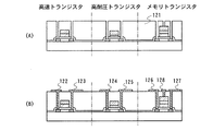
本明細書において、浮遊ゲート電極を有するメモリ素子をメモリトランジスタ、ゲート絶縁膜が2層からなるトランジスタを高耐圧トランジスタ、メモリトランジスタの第1ゲート絶縁膜(浮遊ゲート電極と活性層との間に挟持されたゲート絶縁膜)と同じ程度の膜厚を持ったゲート絶縁膜を有するトランジスタを高速トランジスタと呼ぶ。メモリトランジスタは、情報を書き込んだり読み出したりでき、書き込んだ情報の消去ができる場合もある。高耐圧トランジスタは、メモリトランジスタにかかる電圧と同程度の高電圧がかかかるトランジスタであって、高電圧がかかっても破壊されない程度の膜厚の厚いゲート絶縁膜を有する。高速トランジスタは、高速動作を行うトランジスタであって、デコーダ等の周辺回路を構成するトランジスタである。 In this specification, a memory element having a floating gate electrode is a memory transistor, a transistor having two gate insulating films is a high breakdown voltage transistor, and a first gate insulating film of the memory transistor is sandwiched between the floating gate electrode and the active layer. A transistor having a gate insulating film having the same film thickness as the gate insulating film) is called a high-speed transistor. The memory transistor can write and read information, and can erase the written information. The high breakdown voltage transistor is a transistor to which a high voltage comparable to that applied to the memory transistor is applied, and has a thick gate insulating film that is not destroyed even when a high voltage is applied. The high-speed transistor is a transistor that performs high-speed operation, and constitutes a peripheral circuit such as a decoder.
なお、本明細書において、半導体記憶装置とは少なくともメモリトランジスタを有するものを言う。また、本明細書において、半導体装置とは少なくとも半導体記憶装置を有するものを言う。 Note that in this specification, a semiconductor memory device means at least a memory transistor. In this specification, a semiconductor device means at least a semiconductor memory device.
本発明は、半導体装置を構成するトランジスタの中で、素子形成時の工程数が多いメモリトランジスタに合わせて、その他の高速トランジスタや高耐圧トランジスタを効率よく作製することで、工程数の増加を抑え、低コストな半導体装置を同一基板上に作製することができる。また、以下のような作用効果も発揮し得る。 The present invention suppresses an increase in the number of processes by efficiently producing other high-speed transistors and high-voltage transistors in accordance with memory transistors that have a large number of processes when forming elements among transistors constituting a semiconductor device. A low-cost semiconductor device can be manufactured over the same substrate. Moreover, the following effects can also be exhibited.
メモリトランジスタの第1及び第2ゲート絶縁膜のそれぞれに相当する第1及び第2絶縁膜を積層させて、膜厚の厚い高耐圧トランジスタのゲート絶縁膜とする。これにより、工程数を増加させることなく高耐圧トランジスタのゲート絶縁膜を形成することができる。また、高耐圧トランジスタのゲート絶縁膜を異なる材料の層で積層させて形成できるので、所望の容量を有し且つ高耐圧性を持つトランジスタが形成できる。 The first and second insulating films corresponding to the first and second gate insulating films of the memory transistor are stacked to form the gate insulating film of the thick high voltage transistor. Thereby, the gate insulating film of the high breakdown voltage transistor can be formed without increasing the number of steps. In addition, since the gate insulating film of the high breakdown voltage transistor can be formed by stacking layers of different materials, a transistor having a desired capacitance and high breakdown voltage can be formed.
また、メモリトランジスタの浮遊ゲート電極及び制御ゲート電極のそれぞれが形成される第1び第2導電膜を積層させて、高速トランジスタのゲート電極を形成する。これにより、工程数を増加させることなく高速トランジスタのゲート電極を形成することができる。さらに、高速トランジスタのゲート電極を様々な形状に加工ができるため、低濃度ドレイン(LDD:Lightly Doped Drain)構造というチャネル領域の外側に低濃度の不純物領域を設けた構成をとることができる。この低濃度の不純物領域のことをLDD領域と呼ぶが、特にLDD領域がゲート絶縁膜を介してゲート電極と重なる構造(GOLD(Gate−drain Overlapped LDD)構造)を形成することができる。このような構造をとることにより、トランジスタの耐圧性を向上させたり、信頼性を向上させたりできる。 In addition, the first and second conductive films on which the floating gate electrode and the control gate electrode of the memory transistor are formed are stacked to form the gate electrode of the high-speed transistor. Thereby, the gate electrode of the high-speed transistor can be formed without increasing the number of steps. Further, since the gate electrode of the high-speed transistor can be processed into various shapes, a structure in which a low-concentration impurity region is provided outside the channel region, which is a lightly doped drain (LDD) structure, can be employed. This low-concentration impurity region is referred to as an LDD region. In particular, a structure (GOLD (Gate-drain Overlapped LDD) structure) in which the LDD region overlaps with the gate electrode through the gate insulating film can be formed. With such a structure, the withstand voltage of the transistor can be improved and the reliability can be improved.
さらに、高速トランジスタのゲート電極が2層であるため、ゲート電極として最適な仕事関数を有するゲート電極材料と、引き回しするための低抵抗なゲート電極材料を組み合わせて、ゲート電極を作ることができる。従って、低抵抗で所望のしきい値を持つ高速トランジスタが得られると共に、ゲート電極として用いる材料の幅も広がる。 Further, since the gate electrode of the high-speed transistor has two layers, a gate electrode can be formed by combining a gate electrode material having an optimal work function as a gate electrode and a low-resistance gate electrode material for routing. Accordingly, a high-speed transistor having a low resistance and a desired threshold value can be obtained, and the width of the material used as the gate electrode is widened.
また、本発明は、第2導電膜を成膜した後に行われる導電膜や絶縁膜のエッチングを、各トランジスタにつき同一の一つのレジストマスクを用いてエッチングできる。つまり、エッチングする毎に新たにレジストマスクを形成する必要がないので、レジストマスクの形成が一度で済み工程の短縮化につながる。具体的に、メモリトランジスタにおいては、制御ゲート電極及び浮遊ゲート電極形成のためのエッチング、第2絶縁膜のエッチングを一つのレジストマスクにより行うことができる。高耐圧トランジスタにおいては、ゲート電極形成のためのエッチングと第2絶縁膜のエッチングを一つのレジストマスクにより行うことができる。高速トランジスタにおいては、上部及び下部ゲート電極形成のためのエッチングを一つのレジストマスクにより行うことができる。 In addition, according to the present invention, etching of the conductive film and the insulating film performed after forming the second conductive film can be performed using the same resist mask for each transistor. That is, since it is not necessary to form a new resist mask each time etching is performed, the resist mask needs to be formed only once, leading to shortening of the process. Specifically, in the memory transistor, the etching for forming the control gate electrode and the floating gate electrode and the etching of the second insulating film can be performed with one resist mask. In the high voltage transistor, the etching for forming the gate electrode and the etching of the second insulating film can be performed with one resist mask. In a high-speed transistor, etching for forming the upper and lower gate electrodes can be performed with one resist mask.
さらに、第1導電膜をエッチングして、高耐圧トランジスタの活性層上の第1絶縁膜を露出させると共に、高速トランジスタの活性層及びメモリトランジスタの活性層上部に、第1導電膜のパターン(下部ゲート電極となる膜、浮遊ゲート電極となる膜)をそれぞれ形成する。そのときに、下部ゲート電極となる膜及び浮遊ゲート電極となる膜を、高速トランジスタの活性層及びメモリトランジスタの活性層より一回り大きい形状にするため、以降の工程で生じるプラズマダメージから、第1絶縁膜でなる薄膜のゲート絶縁膜を防ぐことができる。 Further, the first conductive film is etched to expose the first insulating film on the active layer of the high breakdown voltage transistor, and the pattern of the first conductive film (lower part) is formed on the active layer of the high speed transistor and the active layer of the memory transistor. A film to be a gate electrode and a film to be a floating gate electrode). At that time, in order to make the film serving as the lower gate electrode and the film serving as the floating gate electrode slightly larger than the active layer of the high-speed transistor and the active layer of the memory transistor, the first damage is caused by plasma damage caused in the subsequent steps. A thin gate insulating film made of an insulating film can be prevented.
以下、発明を実施するための最良の形態について図面を参照しながら説明する。但し、本発明は多くの異なる態様で実施することが可能であり、本発明の趣旨及びその範囲から逸脱することなくその形態及び詳細を様々に変更し得ることは当業者であれば容易に理解される。従って、本発明は本実施の形態の記載内容に限定して解釈されるものではない。また、各図面において共通の部分は同じ符号を付して詳しい説明を省略する。 The best mode for carrying out the invention will be described below with reference to the drawings. However, the present invention can be implemented in many different modes, and those skilled in the art can easily understand that the modes and details can be variously changed without departing from the spirit and scope of the present invention. Is done. Therefore, the present invention should not be construed as being limited to the description of the embodiment modes. In the drawings, common portions are denoted by the same reference numerals, and detailed description thereof is omitted.
(実施形態1)
図1〜図3は本発明に係る半導体記憶装置の作製工程を示す図である。
(Embodiment 1)
1 to 3 are views showing a manufacturing process of a semiconductor memory device according to the present invention.
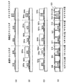
図1(A)の基板101として、例えば石英基板、セラミックス基板、プラスチック基板、ステンレス基板、合成樹脂基板、可撓性基板等がある。これらの基板を用いる際に、基板に接する下地膜(図示せず)を要する場合は適宜用いれば良く、本明細書では下地膜が成膜された基板も含めて基板と呼ぶ。
As the
基板101に接して半導体膜を形成する。形成される半導体膜は、減圧熱CVD法、プラズマCVD法またはスパッタ法などの成膜法で形成される非晶質半導体膜を、レーザー結晶化法で結晶化した結晶性半導体を用いることが望ましい。また、前記成膜法で形成される非晶質半導体膜を熱処理による固相成長法で結晶化した結晶性半導体膜を用いたり、加熱処理した後にレーザー照射をして結晶化した結晶性半導体膜を用いたりしても良い。また、シラン(SiH4)を原料として形成される微結晶半導体膜をレーザー結晶化した結晶性半導体膜でも良い。なお微結晶半導体膜を用いても良い。ここで適用される半導体材料は、シリコン(Si)、ゲルマニウム(Ge)、またシリコンゲルマニウム合金、炭化シリコンがあり、その他にガリウム砒素などの化合物半導体材料を用いることもできる。本形態では結晶性珪素膜を半導体膜として成膜する。また、SOI(Silicon on Insulator)基板を用いて半導体膜を形成しても良い。
A semiconductor film is formed in contact with the
その後、しきい値を制御するためにチャネルドープを行う。本形態では、加速電圧25kV、材料ガスとしてB2H6を用いて行う。 Thereafter, channel doping is performed to control the threshold value. In this embodiment, the acceleration voltage is 25 kV and B 2 H 6 is used as the material gas.
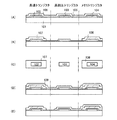
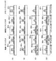
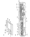
次に、半導体膜をパターニングし、活性層102〜104を形成する。活性層102は高速トランジスタを構成する半導体層、活性層103は高耐圧トランジスタを構成する半導体層、活性層104はメモリトランジスタを構成する半導体層である。これら活性層上に第1絶縁膜105として酸化珪素膜を成膜する。酸化珪素膜をゲート絶縁膜とすると、ゲート絶縁膜と活性層の珪素膜との界面準位が低くなる利点がある。また、第1絶縁膜105は、高速トランジスタではゲート絶縁膜、メモリトランジスタではトンネル酸化膜である第1ゲート絶縁膜として機能するため、膜厚が薄いほど高速動作が可能となり、トンネル電流も流れやすくなる。従って、第1絶縁膜105は薄く成膜できれば如何なる方法を用いても良いが、石英基板等の耐熱性基板ならば、均一に薄く形成できる熱酸化膜が適当である。第1絶縁膜105の膜厚は1〜100nm、好ましくは1〜10nmとする。
Next, the semiconductor film is patterned to form
続いて第1絶縁膜105上に第1導電膜106を成膜する(図1(A))。第1導電膜106として、例えば金属膜や不純物がドープされた半導体膜を用いることができ、導電性を有する膜であれば良い。半導体膜を用いる場合は結晶性半導体膜や微結晶半導体膜があり、その半導体材料、成膜法は活性層102〜104が形成される上記半導体膜と同様なものが考えられる。本形態では第1導電膜106として、窒化タンタル(TaN)膜またはタンタル(Ta)膜を用いる。その後、第1導電膜106はエッチングされ、高速トランジスタの下部ゲート電極となる膜107と、後に浮遊ゲート電極となる膜108が形成される。同時に、高耐圧トランジスタの活性層103上の第1導電膜は除去され、その下の第1絶縁膜が露出する(図1(B))。
Subsequently, a first
なお、このときに第1導電膜106の材料として第1絶縁膜105とエッチング選択比が十分大きなものを用いることが望ましい。例えば第1導電膜106を窒化タンタル膜もしくはタンタル膜とし、第1絶縁膜105を酸化珪素膜とした場合、エッチングガスとしてCl2を用いることで、第1導電膜106の第1絶縁膜に対するエッチング選択比を10以上とすることができ、露出される第1絶縁膜105のオーバーエッチングを防ぐことができる。
At this time, it is desirable to use a material having a sufficiently large etching selectivity with respect to the first insulating
加えて、第1導電膜106の膜厚を薄くすれば、第1導電膜のエッチング時間が少なくなるので、活性層103上の第1絶縁膜105のオーバーエッチングを抑えることができる。さらに第1導電膜の膜厚が薄いと、次に成膜する第2絶縁膜の膜被覆性(カバレッジ)も良くなり、第2絶縁膜上部に形成される制御ゲート電極のエッチングにおいて下地段差の影響が低減される。以上より、第1導電膜106の膜厚は5〜100nm、好ましくは5〜20nmが良い。
In addition, if the thickness of the first
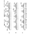
図1(C)は、図1(B)の各活性層102〜104とその上にある下部ゲート電極となる膜107及び浮遊ゲート電極となる膜108の位置関係を示す上面図である。下部ゲート電極となる膜107は活性層102の形状よりも縦横ともに一回り大きい形状にエッチングされる。これにより、高速トランジスタの活性層102及び高速トランジスタの第1絶縁膜部分(高速トランジスタのゲート絶縁膜)を下部ゲート電極となる膜107で覆うようになっている。これは、後に行われるプラズマ工程のプラズマダメージから高速トランジスタの第1絶縁膜部分(高速トランジスタのゲート絶縁膜として機能する部分)を防ぐためである。また、高速トランジスタのゲート絶縁膜は非常に薄く、少しのダメージでも膜に欠陥が生じやすいので、プラズマダメージを防ぐのは非常に有益である。
FIG. 1C is a top view showing a positional relationship between each of the
下部ゲート電極となる膜107と同様に、浮遊ゲート電極となる膜108も活性層104の形状よりも縦横ともに一回り大きい形状にエッチングされ、メモリトランジスタの活性層104及びメモリトランジスタの第1絶縁膜部分(メモリトランジスタの第1ゲート絶縁膜として機能する部分)を浮遊ゲート電極となる膜108で覆うようになっている。これにより、プラズマダメージから第1絶縁膜105を防ぐことができ、第1ゲート絶縁膜内に発生する欠陥を抑えることができる。第1ゲート絶縁膜に一箇所でも欠陥があると、浮遊ゲート電極に蓄積された電荷は全てその欠陥からリークしてしまうため、メモリトランジスタの電荷保持特性に大きく影響するが、本発明はその心配がいらない。
Similar to the
さらに、膜108のチャネル幅方向(図1(C)における縦方向)の長さは、後に行われる浮遊ゲート電極を形成するためのエッチングを経ても、そのまま長さは保持される。従って、大きな浮遊ゲート電極の面積を保持できるため、膜108のチャネル幅方向を長くすることは、メモリトランジスタ動作時の電荷の注入・消去効率の最適化には有効である。
Further, the length of the
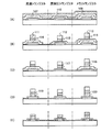
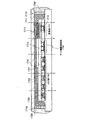
次に、下部ゲート電極となる膜107、浮遊ゲート電極となる膜108、及び露出した第1絶縁膜(下部ゲート絶縁膜)上に第2絶縁膜109を形成する(図1(D))。その後、高速トランジスタにのみ不必要な第2絶縁膜を除去するため、膜107上の第2絶縁膜をエッチング除去して、膜107を露出させる(図1(E))。第2絶縁膜として、第1絶縁膜と同じ材料でなくても良いが、本形態では酸化珪素膜を用いる。この第2絶縁膜のエッチング方法として、CHF3ガスを用いたプラズマエッチングをすることにより、第1導電膜の窒化タンタルまたはタンタルと第2絶縁膜の酸化珪素膜との選択比を10以上にすることができる。また、フッ酸を用いたウェットエッチングであっても、窒化タンタルまたはタンタルとの選択比を十分に大きくとることができる。ここで、高速トランジスタのゲート絶縁膜は下部ゲート電極となる膜107によって覆われているので、第2絶縁膜除去に伴うプラズマダメージを受けることはない。
Next, a second
本形態では第2絶縁膜に第1絶縁膜と同じ酸化珪素膜を用いたが、酸化珪素膜よりも誘電率が大きい窒化珪素膜や、窒化珪素膜を含む膜(SiO2/SiN/SiO2)を用いても良い。なぜなら、酸化珪素膜よりも誘電率の大きい窒化珪素膜を、第2絶縁膜として成膜すると、所望の容量を持ち且つ所望の膜厚のゲート絶縁膜を有する高耐圧トランジスタを作製できるからである。 In this embodiment, the same silicon oxide film as the first insulating film is used as the second insulating film, but a silicon nitride film having a dielectric constant larger than that of the silicon oxide film or a film including a silicon nitride film (SiO 2 / SiN / SiO 2 ) May be used. This is because when a silicon nitride film having a dielectric constant larger than that of the silicon oxide film is formed as the second insulating film, a high voltage transistor having a desired capacitance and a gate insulating film having a desired thickness can be manufactured. .
例えば、第1及び第2絶縁膜を酸化珪素膜で形成して、高耐圧トランジスタのゲート絶縁膜である酸化珪素膜の膜厚を厚くしたとする。すると、トランジスタは一般的に所望の容量を持つように設計されているが、C=ε×S/d(C:容量、ε:誘電率、S:電極面積、d:膜厚)より、誘電率εと電極面積Sが一定のときは、容量Cが小さくなってしまう。しかし、積層される第2導電膜が第1導電膜の酸化珪素膜よりも誘電率εが大きい膜であれば、トランジスタとしての容量は変化させずに、膜厚を厚くすることができるので、容量、ゲート絶縁膜の厚さ共に所望の値である高耐圧トランジスタを作製することができる。つまり、積層構造のゲート絶縁膜を有することで、所望の容量及び高耐圧性を有するトランジスタとすることができる。 For example, it is assumed that the first and second insulating films are formed of silicon oxide films, and the thickness of the silicon oxide film that is the gate insulating film of the high voltage transistor is increased. Then, the transistor is generally designed to have a desired capacitance, but C = ε × S / d (C: capacitance, ε: dielectric constant, S: electrode area, d: film thickness). When the rate ε and the electrode area S are constant, the capacitance C becomes small. However, if the second conductive film to be stacked is a film having a dielectric constant ε larger than that of the silicon oxide film of the first conductive film, the film thickness can be increased without changing the capacitance as a transistor. A high voltage transistor having a desired value for both the capacitance and the thickness of the gate insulating film can be manufactured. In other words, a transistor having a desired capacitance and high withstand voltage can be obtained by including a gate insulating film having a stacked structure.
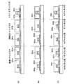
その後、図2(A)に図示するとおり、第2導電膜110を下部ゲート電極となる膜107及び第2絶縁膜109上に形成する。第2導電膜110は、第1導電膜同様、導電性を有する膜であれば良く、本形態ではタングステン(W)膜を用いる。
Thereafter, as shown in FIG. 2A, a second
次に、第2導電膜110上にレジストを形成し、レジストマスク111〜113を形成する。第2導電膜110はレジストマスク111〜113を用いてエッチングされ、高速トランジスタの上部ゲート電極114、高耐圧トランジスタのゲート電極115、メモリトランジスタの制御ゲート電極116が形成される。タングステン膜のエッチングは、CF4、Cl2、O2またはSF6、Cl2、O2の混合ガスを用いて行うことができ、第1導電膜の窒化タンタル膜またはタンタル膜との選択比を5以上にすることができる(図2(B))。
Next, a resist is formed over the second
この際に第2導電膜を用いて配線の引き回しも行う。ここで、第1導電膜を用いて引き回しを行うとすると、上述したように、第1導電膜は薄く成膜しなければならないため、配線抵抗を小さくできない。従って、膜厚に特に制限のない第2導電膜を用いて配線の引き回しを行うのが望ましい。特に、第2導電膜材料であるタングステンは、第1導電膜材料である窒化タンタルまたはタンタルと比較すると、抵抗値が10分の1程度低いため、配線の引き回しには最適である。 At this time, wiring is also routed using the second conductive film. Here, when routing is performed using the first conductive film, as described above, the first conductive film must be thinly formed, and thus the wiring resistance cannot be reduced. Therefore, it is desirable to route the wiring using the second conductive film with no particular limitation on the film thickness. In particular, tungsten, which is the second conductive film material, has a resistance value that is about 1/10 lower than that of tantalum nitride or tantalum, which is the first conductive film material, and thus is optimal for routing the wiring.
また、第1及び第2導電膜を同一材料から形成しても良いが、異なる材料で形成すると以下のような作用がある。一般的に、最適な仕事関数を有するゲート電極材料を用いてゲート電極を形成することで、トランジスタのしきい値をコントロールしている。しかし、中には仕事関数は最適だが高抵抗なゲート電極材料もあり、その場合は配線の引き回しには適さないため、ゲート電極材料としては用いにくい。このような場合にゲート電極が2層であると、下部ゲート電極には仕事関数が最適な材料を用い、上部ゲート電極では低抵抗な材料を用いることができるため、ゲート電極材料として用いることができる材料の幅が広がり、全体として、低抵抗で所望のしきい値の高速トランジスタを得ることができる。 The first and second conductive films may be formed from the same material, but when formed from different materials, the following effects are obtained. In general, the threshold value of a transistor is controlled by forming a gate electrode using a gate electrode material having an optimal work function. However, some gate electrode materials have an optimum work function but a high resistance, and in that case, they are not suitable for routing the wiring, and thus are difficult to use as a gate electrode material. In such a case, if the gate electrode has two layers, a material having an optimum work function can be used for the lower gate electrode, and a low resistance material can be used for the upper gate electrode. The range of materials that can be expanded is wide, and as a whole, a high-speed transistor having a low resistance and a desired threshold value can be obtained.
次に、レジストマスク112及び113を用いて第2絶縁膜をエッチングする(図2(C))。このとき、CHF3を用いたドライエッチングをすることにより、浮遊ゲート電極となる膜108の窒化タンタルまたはタンタルに対して、第2絶縁膜である酸化珪素膜のエッチングレートを10倍以上にすることができる。また、フッ酸を用いたウェットエッチングでも、同様のエッチングレートは得られる。このため、当該エッチングにおける、下部ゲート電極となる膜107と浮遊ゲート電極となる膜108の膜厚差はほとんどできないので、次工程である膜107と108のエッチングを同一の時間内で終えることができ、第1絶縁膜のオーバーエッチングを防ぐことに繋がる。当該エッチングにより、第2絶縁膜からなるパターン117及び118を形成する。パターン117は高耐圧トランジスタの上部ゲート絶縁膜として機能し、パターン118はメモリトランジスタの第2ゲート絶縁膜として機能する。第2絶縁膜である酸化珪素膜は、浮遊ゲート電極材料であり窒化タンタルまたはタンタルと十分なエッチング選択比が取れるため、無用に浮遊ゲート電極となる膜108、さらにはその下の第1絶縁膜105をエッチングすることなく、エッチング後の第1絶縁膜残膜が高速トランジスタおよびメモリトランジスタで揃えることが出来る。
Next, the second insulating film is etched using the resist
次に、下部ゲート電極となる膜107及び浮遊ゲート電極となる膜108を、レジストマスク111及び113を用いてエッチングを行い、高速トランジスタの下部ゲート電極119及び浮遊ゲート電極120を形成する(図2(D))。これら窒化タンタルまたはタンタルからなる膜107及び108のエッチングは、エッチングガスとしてCl2を用いれば、第1絶縁膜の酸化珪素膜との選択比を10以上にすることができる。このため、例え下部ゲート電極となる膜107と浮遊ゲート電極となる膜108に膜厚差があり、どちらか一方の第1絶縁膜がオーバーエッチングされたとしても、その絶対量は大きくないので実質的に問題にはならない。
Next, the
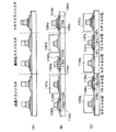
レジストマスク111〜113を除去した後、不純物元素を活性層102〜104にドーピングして、各活性層にソース領域及びドレイン領域を形成する(図2(E))。高耐圧トランジスタの第1ゲート絶縁膜は、図1(B)における第1導電膜のエッチングの際に、幾分エッチングされるかもしれないが、その膜厚はほとんどメモリトランジスタの第1ゲート絶縁膜の膜厚と変わらない。従って、ドーピングは、同じ膜厚の第1絶縁膜を介して全てのトランジスタを一括で行うことが可能となり、ドーピング工程の増加を抑えたトランジスタの作り分けができる。
After removing the resist
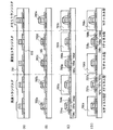
以上のように、不純物領域の形成が完成したら、各トランジスタの第2導電膜からなる上部ゲート電極114、ゲート電極115、制御ゲート電極116を覆うように50nmの酸化珪素膜からなるキャップ膜を形成し、加熱処理、レーザーアニール、又はランプアニール等により、不純物元素の活性化を行う。次に、膜中に水素を含む窒化珪素膜を100nm成膜して、水素化のための熱処理を行う。この熱処理により、窒化珪素膜から放出された水素が、第1及び第2絶縁膜や各活性層中に存在するダングリングボンドといった欠陥を終端したり、膜の界面における界面準位を低減させたりする。
As described above, when the formation of the impurity regions is completed, a cap film made of a 50 nm silicon oxide film is formed so as to cover the
次に、窒化珪素膜上に再び酸化珪素膜を形成して、酸化珪素膜、窒化珪素膜、酸化珪素膜からなる層間絶縁膜121を完成させる。図3(A)では表面が平坦な層間絶縁膜121が図示されているが、平坦でなくとも良い。また、層間絶縁膜としては、窒化珪素膜、酸化珪素膜、窒化酸化珪素膜、有機性樹脂膜の単層、またはそれらを組み合わせた積層膜で形成しても良い。層間絶縁膜の上に何層も配線を設ける場合は、表面を平坦化させた平坦化膜を層間絶縁膜として用いるのが望ましい。その後、層間絶縁膜121に活性層102〜104に達するコンタクトホールと、制御ゲート電極116に達するコンタクトホールを形成する(図3A))。
Next, a silicon oxide film is formed again on the silicon nitride film to complete an
次に、アルミニウム膜や銅等の金属の導電膜を形成・パターニングし、活性層102〜104のソース領域及びドレイン領域と接続する配線122〜127、制御ゲート電極116と接続する配線128を形成する(図3(B))。以上の工程により、半導体記憶装置は完成となる。
Next, a conductive film made of a metal such as an aluminum film or copper is formed and patterned to form
以上のような工程により、浮遊ゲート電極を有するメモリトランジスタ、ゲート絶縁膜が積層されている高耐圧トランジスタ、メモリトランジスタのトンネル酸化膜と同じ膜厚のゲート絶縁膜を有する高速トランジスタを、同一基板上に効率良く、工程数を抑えた作製方法で作製できる。 Through the above process, a memory transistor having a floating gate electrode, a high breakdown voltage transistor in which a gate insulating film is stacked, and a high-speed transistor having a gate insulating film having the same thickness as the tunnel oxide film of the memory transistor are formed on the same substrate. And can be manufactured by a manufacturing method with a reduced number of steps.
なお、この工程で作製した高耐圧トランジスタのゲート絶縁膜は、おおよそメモリトランジスタの第1ゲート絶縁膜と第2ゲート絶縁膜とを足した程度の膜厚を有する。高耐圧トランジスタのゲート絶縁膜は、メモリトランジスタにかかる電圧で破壊されない程度であればいいので、メモリトランジスタの第1ゲート絶縁膜の膜厚以上、好ましくは第1ゲート絶縁膜の膜厚と第2ゲート絶縁膜の膜厚を足した程度の膜厚を有するのが良い。 Note that the gate insulating film of the high-breakdown-voltage transistor manufactured in this step has a film thickness that is approximately the sum of the first gate insulating film and the second gate insulating film of the memory transistor. The gate insulating film of the high breakdown voltage transistor only needs to be of a level that is not destroyed by the voltage applied to the memory transistor. Therefore, the gate insulating film is not less than the thickness of the first gate insulating film of the memory transistor, preferably the first gate insulating film and the second It is preferable to have a film thickness that is approximately the sum of the gate insulating film.
また、メモリトランジスタは浮遊ゲート電極サイズを最適化することで、メモリトランジスタ動作時の電荷の注入・消去効率が最適化される。 Further, by optimizing the size of the floating gate electrode of the memory transistor, the charge injection / erase efficiency during the operation of the memory transistor is optimized.
本作製プロセスは、メモリトランジスタ及び高速トランジスタ共に、最も特性の高さが要求される高速トランジスタのゲート絶縁膜及びメモリトランジスタの第1ゲート絶縁膜を、同一の第1絶縁膜から形成でき、その膜質、膜厚を共用できるという利点がある。 In this manufacturing process, both the memory transistor and the high-speed transistor can form the gate insulating film of the high-speed transistor and the first gate insulating film of the memory transistor, which require the highest characteristics, from the same first insulating film. There is an advantage that the film thickness can be shared.
本形態では、同一基板上に高速トランジスタ、高耐圧トランジスタ、メモリトランジスタを同時に形成する作製プロセスを紹介したが、これに限らず、メモリトランジスタと高速トランジスタ、メモリトランジスタと高耐圧トランジスタといった2種類のトランジスタを組み合わせて同一基板上に同時に形成しても良い。 In this embodiment mode, a manufacturing process in which a high-speed transistor, a high breakdown voltage transistor, and a memory transistor are simultaneously formed on the same substrate has been introduced. However, the present invention is not limited to this, and two types of transistors such as a memory transistor and a high-speed transistor May be simultaneously formed on the same substrate.
(実施形態2)
図4は本発明に係る半導体記憶装置の作製工程を示す図である。図4において、図1〜図3と対応する部分については同じ符号を用い、その詳細な説明として実施形態1の説明を参照する。
(Embodiment 2)
FIG. 4 is a diagram showing a manufacturing process of the semiconductor memory device according to the present invention. 4, the same reference numerals are used for portions corresponding to those in FIGS. 1 to 3, and the description of the first embodiment is referred to as a detailed description thereof.
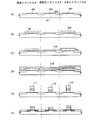
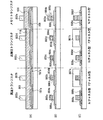
図4の基板401としては、単結晶のシリコンからなる半導体基板を用いるが、SOI(Silicon on Insulator)基板を用いて半導体膜を形成しても良い。次に、しきい値を制御するためにチャネルドープを行う。本形態では、加速電圧25kVで材料ガスとしてB2H6を用いて行う。
As the
次に、LOCOS法(選択酸化法)やSTI法(Shallow Trench Isolation)等の公知のアイソレーション技術により素子分離を行い、半導体基板表面に活性層402〜404を形成する。活性層402は高速トランジスタを構成する半導体層であり、活性層403は高耐圧トランジスタを構成する半導体層であり、活性層404はメモリトランジスタを構成する半導体層である。次に熱酸化を行い、半導体基板上に接して熱酸化膜を形成し、第1絶縁膜405とする。熱酸化膜は薄く均一に形成できるので第1絶縁膜としては最適である(図4(A))。しかし、熱酸化膜に限らず、その他の成膜法を用いて第1絶縁膜を形成しても良い。
Next, element isolation is performed by a known isolation technique such as a LOCOS method (selective oxidation method) or an STI method (Shallow Trench Isolation) to form
続いて第1絶縁膜上に第1導電膜106として窒化タンタル(TaN)膜またはタンタル膜(Ta)を成膜する。その後、エッチングして、下部ゲート電極となる膜107、浮遊ゲート電極となる膜108を形成し、活性層403上の第1絶縁膜を露出させる(図4(B))。次に、下部ゲート電極となる膜107、浮遊ゲート電極となる膜108、露出した第1絶縁膜上に、第2絶縁膜109として酸化珪素膜を形成する。第2絶縁膜109を形成後、下部ゲート電極となる膜107上にある第2絶縁膜のみをエッチング除去する(図4(C))。
Subsequently, a tantalum nitride (TaN) film or a tantalum film (Ta) is formed as the first
その後、図4(D)に図示するとおり、タングステン(W)膜である第2導電膜110を下部ゲート電極となる膜107及び第2絶縁膜109上に形成する。
Thereafter, as illustrated in FIG. 4D, a second
次に第2導電膜110上にレジストを形成した後に、レジストマスク111〜113を形成する。第2導電膜110、第2絶縁膜109、下部ゲート電極となる膜107、浮遊ゲート電極となる膜108はレジストマスク111〜113を用いて順にエッチングされ、各トランジスタのゲート電極を形成する(図4(E))。
Next, after forming a resist on the second
次に、レジストマスク111〜113を除去した後、不純物元素を活性層にドーピングしてソース領域及びドレイン領域を形成する(図4(F))。その後は、加熱処理、レーザーアニール、ランプアニール等により、不純物元素の活性化を行う。
Next, after removing the resist
これ以降の工程は図3と同様、層間絶縁膜を形成して、コンタクトホールを形成し、各半導体層及び制御ゲート電極に接続する配線を形成して完成となる。 The subsequent steps are completed by forming an interlayer insulating film, forming contact holes, and forming wirings connected to the respective semiconductor layers and control gate electrodes, as in FIG.
以上のような工程により、浮遊ゲート電極を有するメモリトランジスタ、ゲート絶縁膜が積層されている高耐圧トランジスタ、メモリトランジスタのトンネル酸化膜と同じ膜厚のゲート絶縁膜を有する高速トランジスタを、同一基板上に効率良く、工程数を抑えた作製方法で作製できる。 Through the above process, a memory transistor having a floating gate electrode, a high breakdown voltage transistor in which a gate insulating film is stacked, and a high-speed transistor having a gate insulating film having the same thickness as the tunnel oxide film of the memory transistor are formed on the same substrate. And can be manufactured by a manufacturing method with a reduced number of steps.
本形態では、同一基板上に高速トランジスタ、高耐圧トランジスタ、メモリトランジスタを同時に形成する作製プロセスを紹介したが、これに限らず、メモリトランジスタと高速トランジスタ、メモリトランジスタと高耐圧トランジスタといった2種類のトランジスタを組み合わせて同一基板上に同時に形成しても良い。 In this embodiment mode, a manufacturing process in which a high-speed transistor, a high breakdown voltage transistor, and a memory transistor are simultaneously formed on the same substrate has been introduced. However, the present invention is not limited to this, and two types of transistors such as a memory transistor and a high-speed transistor May be simultaneously formed on the same substrate.
メモリトランジスタをNチャネル型トランジスタ、高速トランジスタをPチャネル型及びNチャネル型トランジスタ、高耐圧トランジスタをPチャネル型及びNチャネル型トランジスタで構成する半導体記憶装置の作製方法について説明する。また、下記実施例1〜4において様々な本発明の例を図面を用いて示すが、各図面において上記実施形態と共通の部分は同じ符号を付し、その詳細な説明として実施形態1の説明を参照する。
A method for manufacturing a semiconductor memory device in which a memory transistor is an N-channel transistor, a high-speed transistor is a P-channel transistor and an N-channel transistor, and a high breakdown voltage transistor is a P-channel transistor and an N-channel transistor is described. In the following Examples 1 to 4, various examples of the present invention will be described with reference to the drawings. In each drawing, the same reference numerals are given to the same parts as those in the above embodiment, and the description of
本実施例は、各素子のゲート電極等を形成するまでは前述した図1(A)〜図2(D)と同様な作製工程なので、図2(D)以降の工程について図5を用いて以下に説明する。 Since this example is a manufacturing process similar to that of FIGS. 1A to 2D described above until the gate electrode and the like of each element are formed, the process after FIG. 2D will be described with reference to FIGS. This will be described below.
図5(A)は、高速トランジスタ、高耐圧トランジスタ、メモリトランジスタの各ゲート電極上から図2(D)で示すレジストマスクを除去した状態を示している。ここに新たにレジストマスク501a、501bを形成する。そして、n型を付与する不純物元素を添加して、n型を呈する不純物領域502a、502b、503a、503b、504a、504bを形成する。なお、n型不純物元素としては、代表的には15族に属する元素、典型的にはリンまたは砒素を用いることができる(図5(B))。
FIG. 5A shows a state where the resist mask shown in FIG. 2D is removed from the gate electrodes of the high-speed transistor, the high breakdown voltage transistor, and the memory transistor. New resist
この不純物領域502a、502b、503a、503b、504a、504bはそれぞれ、Nチャネル型の高速トランジスタのソース領域及びドレイン領域、Nチャネル型の高耐圧トランジスタのソース領域及びドレイン領域、Nチャネル型のメモリトランジスタのソース領域及びドレイン領域である。なお、ここで形成された不純物領域にはn型不純物元素が1×10²⁰〜1×10²¹atoms/cm3(代表的には2×1020〜5×1021atoms/cm3)の濃度で含まれている。本明細書では、n型不純物元素を含む不純物領域をn型不純物領域と定義する。
The
上記n型不純物領域を形成後、レジストマスク501a、501bをウェットエッチングにより剥離して、新たにレジストマスク505a〜cを形成する。そして、p型不純物元素(本実施例ではボロン)を添加して高濃度にボロンを含む不純物領域506a、506b、507a、507bを形成する(図5(C))。本実施例ではジボラン(B2H6)を用いたイオンドープ法により、3×10²⁰〜3×10²¹atoms/cm3(代表的には2×1020〜5×1021atoms/cm3)の濃度でボロンを含む不純物領域を形成する。これら不純物領域は、Pチャネル型の高速トランジスタのソース領域及びドレイン領域、Pチャネル型の高耐圧トランジスタのソース領域及びドレイン領域である。なお、本明細書では、p型不純物元素を含む不純物領域をp型不純物領域と定義する。
After the n-type impurity region is formed, the resist
以上の工程により各トランジスタの活性層に不純物領域を形成した後、レジストマスク505a〜cをウェットエッチングにより剥離する。その後、不純物領域の活性化をし、層間絶縁膜121を形成する。次に、層間絶縁膜121をエッチングしてコンタクトホールを形成し、各トランジスタのn型不純物領域又はp型不純物領域である502a、502b、503a、503b、506a、506b、507a、507b、メモリトランジスタの制御ゲート電極に接続する配線508〜516を形成する(図5(D))。配線材料としては、実施形態1で述べた配線材料と同様のものが用いられる。以上の工程により、半導体記憶装置を完成させる。なお、本実施例は図4で示す半導体基板を用いた半導体記憶装置の作製方法にも応用が可能である。
After the impurity region is formed in the active layer of each transistor through the above steps, the resist
高耐圧トランジスタ及び高速トランジスタが、低濃度不純物領域のLDD領域を有するLDD構造の半導体記憶装置の作製方法について説明する。本実施例は、各トランジスタのゲート電極を形成するまでは前述した図1(A)〜図2(D)と同様な作製工程なので、図2(D)以降の工程について図6及び図7を用いて以下に説明する。 A method for manufacturing a semiconductor memory device having an LDD structure in which a high-breakdown-voltage transistor and a high-speed transistor have an LDD region of a low concentration impurity region is described. Since this embodiment is a manufacturing process similar to that of FIGS. 1A to 2D described above until the gate electrode of each transistor is formed, FIGS. 6 and 7 will be described with respect to the processes after FIG. This will be described below.
高速トランジスタ、高耐圧トランジスタ、メモリトランジスタの各ゲート電極上から図2(D)で示すレジストマスクを除去して、新たにレジストマスク601a〜dを形成する。そして、n型を付与する不純物元素を添加して、メモリトランジスタの活性層にn型不純物領域602a、602bを形成する(図6(A))。なお、n型不純物元素としては、代表的には15族に属する元素、典型的にはリンまたは砒素を用いることができる。
The resist mask shown in FIG. 2D is removed from the gate electrodes of the high-speed transistor, high-voltage transistor, and memory transistor, and new resist
n型不純物領域602a、602bはそれぞれ、Nチャネル型のメモリトランジスタのソース領域及びドレイン領域である。なお、ここで形成されたn型不純物領域にはn型不純物元素が1×10²⁰〜1×10²¹atoms/cm3(代表的には2×1020〜5×1021atoms/cm3)の濃度で含まれている。
The n-
n型不純物領域602a、602bを形成後、レジストマスク601a〜dをウェットエッチングにより剥離して、次にPチャネル型の高速トランジスタ、Pチャネル型の高耐圧トランジスタ、メモリトランジスタを覆うように、レジストマスク603a〜cを形成する。そして、n型不純物元素を添加して低濃度にn型不純物元素(リン)を含むn型不純物領域604a、604b、605a、605bを形成する(図6(B))。こうして形成されたn型不純物領域604a、604b、605a、605bには、代表的には1×10¹⁶〜5×10¹⁸atoms/cm3(典型的には3×1017〜3×1018atoms/cm3)でn型不純物元素が添加されるように調節する。
After the n-
次に、レジストマスク603a〜cをウェットエッチングにより剥離してから、レジストマスク606a〜cを形成し、p型を付与する不純物元素を添加して、低濃度にボロンを含むp型不純物領域607a、607b、608a、608bを形成する(図6(C))。これらp型不純物領域が、1×10¹⁶〜5×10¹⁸atoms/cm3程度の濃度でp型を付与する不純物元素を含むようにボロン(B)を添加する。
Next, after removing the resist
そして、レジストマスク606a〜cをウェットエッチングにより剥離して、酸化珪素膜701を全面に形成する(図7(A))。その後、酸化珪素膜701をエッチバックして、各ゲート電極の側面にサイドウォール702a〜eを形成する(図7(B))。このとき、第1絶縁膜105は酸化珪素膜701と一緒にドライエッチングにさらされるが、実際ゲート絶縁膜として機能する各ゲート電極の真下の部分は、ゲート電極により保護されているため、プラズマダメージを受ける心配はない。
Then, the resist masks 606a to 606c are removed by wet etching to form a
次に、高濃度のリンを添加するため、Pチャネル型の高速トランジスタ及び高耐圧トランジスタ、メモリトランジスタをレジストマスク703a〜cで覆う。そして、リンを添加し、1×10²⁰〜1×10²¹atoms/cm3(代表的には2×1020〜5×1021atoms/cm3)の濃度でn型不純物元素を含むようなn型不純物領域を形成する。この不純物元素の添加により、Nチャネル型の高速トランジスタのソース領域704a及びドレイン領域704b、低濃度不純物領域であるLDD領域704c及び704d、チャネル形成領域704eが形成される。また、Nチャネル型の高耐圧トランジスタのソース領域705a及びドレイン領域705b、LDD領域705c及び705d、チャネル形成領域705eが形成される(図7(C))。
Next, in order to add high-concentration phosphorus, the P-channel high-speed transistor, the high breakdown voltage transistor, and the memory transistor are covered with resist
次に、レジストマスク703a〜cをウェットエッチングにより剥離して、レジストマスク706a〜cを形成する。そして、p型不純物元素を添加して、3×10²⁰〜3×10²¹atoms/cm3の濃度でボロンを含むようにp型不純物領域を形成する。これにより、Pチャネル型の高速トランジスタのソース領域707a及びドレイン領域707b、LDD領域707c及び707d、チャネル形成領域707eが形成される。また、Pチャネル型の高耐圧トランジスタのソース領域708a及びドレイン領域708b、LDD領域708c及び708d、チャネル形成領域708eが形成される(図7(D))。
Next, the resist
以上のような工程により、メモリトランジスタ以外の高速トランジスタ、高耐圧トランジスタをLDD構造にできる。図7(D)以降は、レジストマスク706a〜cを除去し、図5(D)と同様な工程を経て完成となる。本実施例の構成は、LDD構造をとることでトランジスタの耐圧を良くすることができ、また、微細化が進み単チャネル効果が生じたときに、単チャネル効果を抑制することができる。なお、本実施例は図4で示す半導体基板を用いた半導体記憶装置の作製方法にも応用が可能である。
Through the steps as described above, high-speed transistors and high-breakdown-voltage transistors other than the memory transistors can be made into the LDD structure. After FIG. 7D, the resist
本実施例は、実施例2とは別の方法で、LDD構造又はGOLD構造を有する半導体記憶装置の作製方法について説明する。本実施例は、第2導電膜を形成するまでは前述した図1(A)〜図2(A)と同様な作製工程なので、図2(A)以降の工程について図8及び図9を用いて以下に説明する。なお本明細書において、LDD領域がゲート絶縁膜を介してゲート電極と重なる領域をLov領域(第1のLDD領域)と呼び、LDD領域がゲート絶縁膜を介してゲート電極と重ならない領域をLoff領域(第2のLDD領域)と呼ぶ。
In this embodiment, a method for manufacturing a semiconductor memory device having an LDD structure or a GOLD structure will be described by a method different from that in
第2導電膜110を形成した後に、第2導電膜上に酸化珪素膜801を形成する。そして、酸化珪素膜801上にレジストを堆積しパターニングして、レジストマスク802a〜eを形成する(図8(A))。このレジストマスク802a〜eを用いてその下層の酸化珪素膜801をエッチングして酸化珪素膜803a〜eを形成し、次に第2導電膜110をエッチングして上部ゲート電極804a、804b、高耐圧トランジスタのゲート電極804c、804d、制御ゲート電極804eを形成する。さらに、レジストマスク802c〜eを用いて第2絶縁膜109をエッチングして、高耐圧トランジスタの上部ゲート絶縁膜805a、805b、メモリトランジスタの第2ゲート絶縁膜805cを形成する。次に、レジストマスク802a、802b、802eを用いて、下部ゲート電極となる膜107a、107b、浮遊ゲート電極となる膜108をエッチングして、下部ゲート電極806a、806b、浮遊ゲート電極806cを形成する(図8(B))。
After forming the second
図8(A)で示すレジストマスク802a〜eを形成してから、図8(B)の状態になるまで、各膜のエッチングは全てレジストマスク802a〜eのいずれかを用いて行われる。
After the formation of the resist
レジストマスク802a〜eを除去後、新たにレジストマスク807a、807bを形成し、P型チャネルの高速トランジスタ及び高耐圧トランジスタを覆う。次に、n型を付与する不純物元素を添加してn型不純物領域808a〜fを形成する。n型不純物領域808a〜fのn型不純物領域の濃度が1×10²⁰〜1×10²¹atoms/cm3(代表的には2×1020〜5×1021atoms/cm3)になるように形成する。なお、n型不純物元素としては、代表的には15族に属する元素、典型的にはリンまたは砒素を用いることができる(図8(C))。
After removing the resist
次に、レジストマスクを807a〜bをウェットエッチングにより剥離して、レジストマスク901a〜cを形成する。この状態で、p型を付与する不純物元素を高濃度で添加して、p型不純物領域902a〜dを形成する。p型不純物領域902a〜dが、3×10²⁰〜3×10²¹atoms/cm3の濃度でp型不純物元素を含むように、不純物元素を添加する。p型不純物元素としてはボロンを用いることができる(図9(A))。
Next, the resist
その後、レジストマスク901a〜cをウェットエッチングにより剥離する。次に酸化珪素膜803a〜eをマスクとして、上部ゲート電極804a、804b、高耐圧トランジスタのゲート電極804c、804d、制御ゲート電極804eの等方性エッチングを行い、その側面を目減りさせ、横幅の小さくなった上部ゲート電極903a、903b、高耐圧トランジスタのゲート電極903c、903d、制御ゲート電極903eを形成する(図9(B))。次に酸化珪素膜803a〜eを除去し、P型チャネルの高速トランジスタ及び高耐圧トランジスタを覆うレジストマスク904a、904bを形成する。そして、n型を付与する不純物元素を添加し、Nチャネル型の高速トランジスタのソース領域905a及びドレイン領域905b、Lov領域905c及び905d、チャネル形成領域905eを形成する。また、Nチャネル型の高耐圧トランジスタのソース領域906a及びドレイン領域906b、Loff領域906c及び906d、チャネル形成領域906eを形成する。Lov領域905c及び905d、Loff領域906c及び906dは、代表的には1×10¹⁶〜5×10¹⁸atoms/cm3(典型的には3×1017〜3×1018atoms/cm3)のn型不純物元素が添加されるようにする(図9(C))。
Thereafter, the resist
次に、レジストマスク904a、904bをウェットエッチングにより剥離して、レジストマスク907a〜cを形成する。そして、p型不純物元素を低濃度で添加してp型不純物領域を形成する。低濃度p型不純物領域が、1×10¹⁶〜5×10¹⁷atoms/cm3程度の濃度で不純物元素を含むようにボロン(B)を添加する。これにより、Pチャネル型の高速トランジスタのソース領域908a及びドレイン領域908b、Lov領域908c及び908d、チャネル形成領域908eが形成された。また、Pチャネル型の高耐圧トランジスタのソース領域909a及びドレイン領域909b、Loff領域909c及び909d、チャネル形成領域909eが形成された。
Next, the resist
以上のような工程により、高速トランジスタはGOLD構造、高耐圧トランジスタはLDD構造となる。その後、レジストマスク907a〜cをウェットエッチングにより剥離した後に図5(D)と同様な工程を経て完成する。また、上部ゲート電極903a、903bをマスクとして、高速トランジスタの下部ゲート電極806a、806bを上部ゲート電極と同じゲート電極長になるようエッチングすれば、高速トランジスタはLoff領域を有するLDD構造となる。
Through the above process, the high-speed transistor has a GOLD structure, and the high voltage transistor has an LDD structure. After that, the resist masks 907a to 907c are peeled off by wet etching, and the process is completed through a process similar to that shown in FIG. Further, if the
LDD構造は耐圧性が良いトランジスタが得られ、GOLD構造は信頼性が良いトランジスタが得られるため、状況により適した構造を用いれば良い。なお、本実施例は図4で示す半導体基板を用いた半導体記憶装置の作製方法にも応用が可能である。 Since the LDD structure can provide a transistor with good withstand voltage and the GOLD structure can obtain a transistor with good reliability, a structure suitable for the situation may be used. Note that this embodiment can also be applied to a method for manufacturing a semiconductor memory device using the semiconductor substrate shown in FIG.
本実施例は、高速トランジスタ及び高耐圧トランジスタが低濃度不純物領域を有する半導体記憶装置の作製方法について説明する。本実施例は、第2導電膜を形成するまでは前述した図1(A)〜図2(A)と同様な作製工程なので、図2(A)以降の工程について図10及び図11を用いて以下に説明する。 In this embodiment, a method for manufacturing a semiconductor memory device in which a high-speed transistor and a high breakdown voltage transistor have a low concentration impurity region will be described. Since this embodiment is a manufacturing process similar to that of FIGS. 1A to 2A described above until the second conductive film is formed, FIGS. 10 and 11 are used for the processes after FIG. Will be described below.
第2導電膜上にレジストを堆積した後に、レジストマスク1001a〜eを形成する。そして電極を形成するための第1のエッチング処理を行う。エッチングにはICP(Inductive Coupled Plasma:誘導結合型プラズマ)エッチング装置を用いる。第1のエッチング処理には、エッチングガスとしてCF4、Cl2、O2を添加する。エッチング圧力は1.3Paとし、800Wのプラズマ生成用の電力、300Wの基板バイアス用の電力を供給する。このエッチングにより、第2導電膜はテーパー状のパターン1002a〜eとなる(図10(A))。
After a resist is deposited on the second conductive film, resist
次に、第2絶縁膜109の酸化珪素膜を、CHF3ガスを用いたテーパーエッチングにより第2のエッチング処理を行う。これにより第2絶縁膜はテーパー状の上部ゲート絶縁膜1003a、1003b、テーパー状の第2ゲート絶縁膜1003cに加工される(図10(B))。
Next, a second etching process is performed on the silicon oxide film of the second
次に、第3のエッチング処理として、エッチングガスをCF4、Cl2に切り替えて第1導電層である窒化タンタルまたはタンタルのエッチングを行う。この時のエッチング条件は、エッチング圧力1.3Pa、500Wのプラズマ生成用の電力、10Wの基板バイアス用の電力を供給する。以上のようにして、テーパー状の下部ゲート電極1004a、1004b、浮遊ゲート電極1004cを形成することができる(図10(C))。
Next, as a third etching process, the etching gas is switched to CF 4 and Cl 2 to etch tantalum nitride or tantalum that is the first conductive layer. The etching conditions at this time are an etching pressure of 1.3 Pa, 500 W of plasma generation power, and 10 W of substrate bias power. As described above, tapered
次は、エッチングガスにSF6、Cl2、O2を用いてテーパー状のパターン1002a〜eの異方性エッチングを行う。エッチング圧力は1.9Paとし、500Wのプラズマ生成用の電力、3Wの基板バイアス用の電力を供給する。この異方性エッチングにより、テーパー状のパターン1002a〜eの端部は下部ゲート電極1004a、1004b、浮遊ゲート電極1004cやテーパー状の上部ゲート絶縁膜1003a、1003b、テーパー状の第2ゲート絶縁膜1003cよりも内側に後退する(図11(A))。
Next, anisotropic etching is performed on the tapered
レジストマスク1001a〜eを除去した後に、Pチャネル型のトランジスタ上にレジストマスクを1101a、1101bを形成して、1×10¹⁹〜5×10²¹/cm3のリン濃度でイオン注入する。これにより、Nチャネル型の高速トランジスタでは、ソース領域1102a及びドレイン領域1102b、Lov領域1102c及び1102d、チャネル形成領域1102eが一度に形成される。Nチャネル型の高耐圧トランジスタでは、ソース領域1103a及びドレイン領域1103b、Loff領域1103c及び1103d、チャネル形成領域1103eが一度に形成される。メモリトランジスタでは、ソース領域1104a及びドレイン領域1104b、Lov領域1104c及び1104d、チャネル形成領域1104eが一度に形成される(図11(B))。
After removing the resist
次に、レジストマスク1101a、1101bをウェットエッチングにより剥離する。次に、Nチャネル型のトランジスタ及びメモリトランジスタを覆うように、レジストマスク1105a〜cを形成し、1×10¹⁹〜5×10²¹/cm3の不純物濃度(ボロン)でイオン注入する。これにより、Pチャネル型の高速トランジスタでは、ソース領域1106a及びドレイン領域1106b、Lov領域1106c及び1106d、チャネル形成領域1106eが形成される。Pチャネル型の高耐圧トランジスタでは、ソース領域1107a及びドレイン領域1107b、Loff領域1107c及び1107d、チャネル形成領域1107eが形成される(図11(C))。
Next, the resist
以後は、レジストマスク1105a〜cをウェットエッチングにより剥離した後、図5(D)と同様な工程を経て完成となる。また、上部ゲート電極をマスクとして、高速トランジスタの下部ゲート電極のテーパー部分をエッチングすれば、Loff領域を有するLDD構造にもできる。本実施例は、一度の不純物元素の注入により、ソース及びドレイン領域と共にLoff領域、Lov領域を形成できる。また、本実施例の構成は、微細化が進み単チャネル効果が生じたときに、単チャネル効果を抑制することができる。なお、本実施例は図4で示す半導体基板を用いた半導体記憶装置の作製方法にも応用が可能である。
Thereafter, after the resist
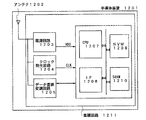
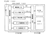
本発明の半導体記憶装置を用いた半導体装置として、CPU(Central Processing Unit)を内蔵する非接触型のICカードあるいはIDタグの典型的なブロック図を図12に示す。同図において、半導体装置1201は、集積回路1211を内蔵し、集積回路1211は、電源回路1203、クロック発生回路1204、データ復調変調回路1205、CPU1207、インターフェース(IFと表記)1208、不揮発性メモリ(NVMと表記)1209、SRAM1210によって構成されている。なお、SRAM1210の代わりに、DRAMなどの揮発性メモリを用いても構わない。
As a semiconductor device using the semiconductor memory device of the present invention, a typical block diagram of a non-contact type IC card or ID tag incorporating a CPU (Central Processing Unit) is shown in FIG. In the figure, a semiconductor device 1201 includes an integrated circuit 1211. The integrated circuit 1211 includes a power supply circuit 1203, a
本実施例においては、不揮発性メモリ1209として本発明の半導体記憶装置を構成するメモリトランジスタを用いる。また、クロック発生回路1204、データ復調変調回路1205、CPU1207、インターフェース1208、SRAM1210を構成するトランジスタとして、高速動作のトランジスタが必要な場合は、本発明の半導体記憶装置を構成する高速トランジスタの作製プロセスで、本発明の半導体記憶装置と同時に作製することができる。電源回路1203を構成するトランジスタとして高耐圧性のトランジスタが必要な場合は、本発明の半導体記憶装置を構成する高耐圧トランジスタの作製プロセスで、本発明の半導体記憶装置と同時に作製することができる。以上より、同一基板上に集積回路を効率よく作製できる。
In this embodiment, a memory transistor constituting the semiconductor memory device of the present invention is used as the
さらに、作製工程が簡略化され、低価格に作製できる本発明の半導体記憶装置を不揮発性メモリ1209に適用できるため、コストの低減及び小型化を実現した半導体装置1201を提供することが可能となる。
In addition, since the manufacturing process can be simplified and the semiconductor memory device of the present invention that can be manufactured at low cost can be applied to the
集積回路1211はガラス基板上、もしくはフレキシブル基板上、半導体基板上に形成されている。アンテナ1202は、半導体装置内の集積回路1211と同一基板上に形成されていても良いし、集積回路上下の保護層に形成されていても良い。このように、集積回路1211と同一基板上にアンテナを形成する場合、ナノ粒子を使った組成物を印刷法(液滴出法やスクリーン印刷法)により形成する方法を用いることもできる。 The integrated circuit 1211 is formed over a glass substrate, a flexible substrate, or a semiconductor substrate. The antenna 1202 may be formed over the same substrate as the integrated circuit 1211 in the semiconductor device, or may be formed in protective layers above and below the integrated circuit. As described above, when an antenna is formed over the same substrate as the integrated circuit 1211, a method of forming a composition using nanoparticles by a printing method (a droplet ejection method or a screen printing method) can also be used.
また、半導体装置は、アンテナとの接続端子だけを設けた集積回路1211と、銅やアルミニウムなどで作成したアンテナ1202とを、異方性導電膜等を用いて電気的に接続しても良い。 In the semiconductor device, the integrated circuit 1211 provided only with a connection terminal to the antenna may be electrically connected to the antenna 1202 made of copper, aluminum, or the like using an anisotropic conductive film or the like.
また、集積回路1211のサイズは5ミリ角以下で、好ましくは0.3ミリ〜4ミリ角の面積を有し、集積回路1211上下の保護層は半導体装置のサイズよりも大きい。 The size of the integrated circuit 1211 is 5 mm square or less, and preferably has an area of 0.3 mm to 4 mm square. The protective layers above and below the integrated circuit 1211 are larger than the size of the semiconductor device.
本実施例は、実施形態1〜2、実施例1〜4と組み合わせて用いることが可能である。 This example can be used in combination with Embodiments 1-2 and Examples 1-4.
本発明の半導体記憶装置を有する非接触型のRFID(Radio Frequency Identification)タグの典型的なブロック図を図13に示す。図13には、認証データ等の固定データを読み出す簡単な機能を有する構成を示した。同図において、RFIDタグ1301は、アンテナ1302、高周波回路1303、電源回路1304、リセット回路1305、クロック発生回路1306、データ復調回路1307、データ変調回路1308、制御回路1309、不揮発性メモリ(NVMと表記)1310、ROM1311によって構成されている。 FIG. 13 shows a typical block diagram of a non-contact RFID (Radio Frequency Identification) tag having the semiconductor memory device of the present invention. FIG. 13 shows a configuration having a simple function of reading fixed data such as authentication data. In the figure, an RFID tag 1301 includes an antenna 1302, a high frequency circuit 1303, a power supply circuit 1304, a reset circuit 1305, a clock generation circuit 1306, a data demodulation circuit 1307, a data modulation circuit 1308, a control circuit 1309, and a nonvolatile memory (NVM). ) 1310 and ROM 1311.
本実施例においては、不揮発性メモリ1310として本発明の半導体記憶装置を構成するメモリトランジスタを用いる。また、高周波回路1303、リセット回路1305、クロック発生回路1306、データ復調回路1307、データ変調回路1308、制御回路1309、ROM1311を構成するトランジスタとして、高速動作をするトランジスタが必要な場合は、本発明の半導体記憶装置を構成する高速トランジスタの作製プロセスで同時に作製することができる。電源回路1304を構成するトランジスタとして高耐圧性のトランジスタが必要な場合は、本発明の半導体記憶装置を構成する高耐圧トランジスタの作製プロセスにより、本発明の半導体記憶装置と同時に作製することができる。以上より、同一基板上にRFIDタグを効率よく作製することが可能となる。 In this embodiment, a memory transistor constituting the semiconductor memory device of the present invention is used as the nonvolatile memory 1310. Further, when a transistor that operates at high speed is required as a transistor constituting the high-frequency circuit 1303, the reset circuit 1305, the clock generation circuit 1306, the data demodulation circuit 1307, the data modulation circuit 1308, the control circuit 1309, and the ROM 1311, The semiconductor memory device can be manufactured at the same time by a manufacturing process of a high-speed transistor constituting the semiconductor memory device. In the case where a high-breakdown-voltage transistor is required as a transistor included in the power supply circuit 1304, the transistor can be manufactured at the same time as the semiconductor memory device of the present invention by a manufacturing process of the high-voltage transistor included in the semiconductor memory device of the present invention. As described above, an RFID tag can be efficiently manufactured on the same substrate.
さらに、作製工程が簡略化され、低価格に作製できる本発明の半導体記憶装置を不揮発性メモリ1310に適用できるため、RFIDタグ1301としてもコストの低減及び小型化を実現することが可能となる。 Furthermore, since the manufacturing process can be simplified and the semiconductor memory device of the present invention that can be manufactured at low cost can be applied to the nonvolatile memory 1310, the RFID tag 1301 can be reduced in cost and size.
また、図13に示した回路は全てガラス基板上、もしくはフレキシブル基板上、半導体基板上に形成されている。アンテナ1302は前記ガラス基板上、もしくはフレキシブル基板上、半導体基板上に形成されていてもよいし、基板の外部にあり、基板内部の半導体集積回路と接続されるものであってもよい。 Further, all the circuits shown in FIG. 13 are formed on a glass substrate, a flexible substrate, or a semiconductor substrate. The antenna 1302 may be formed on the glass substrate, a flexible substrate, or a semiconductor substrate, or may be outside the substrate and connected to a semiconductor integrated circuit inside the substrate.
高周波回路1303はアンテナ1302よりアナログ信号を受信し、またデータ変調回路1308より受け取ったアナログ信号をアンテナ1302から出力する回路である。電源回路1304は受信信号から定電源を生成する回路、リセット回路1305はリセット信号を生成する回路、クロック発生回路1306はクロック信号を発生する回路、データ復調回路1307は受信した信号からデータを抽出する回路、データ変調回路1308は制御回路から受け取ったデジタル信号をもとにアンテナへ出力するアナログ信号を生成、あるいは、アンテナ特性を変化させる回路であり、以上の回路からアナログ部が構成される。 The high frequency circuit 1303 is a circuit that receives an analog signal from the antenna 1302 and outputs the analog signal received from the data modulation circuit 1308 from the antenna 1302. The power supply circuit 1304 generates a constant power supply from the received signal, the reset circuit 1305 generates a reset signal, the clock generation circuit 1306 generates a clock signal, and the data demodulation circuit 1307 extracts data from the received signal. A circuit and data modulation circuit 1308 is a circuit that generates an analog signal to be output to an antenna based on a digital signal received from a control circuit or changes antenna characteristics, and an analog unit is configured by the above circuits.
一方、制御回路1309は受信した信号から抽出したデータを受け取って、データ読み出しを行う。具体的には、不揮発性メモリ1310やROM1311のアドレス信号を生成して、データの読み出しを行ない、読み出したデータをデータ変調回路に送る。以上の回路からデジタル部が構成されている。 On the other hand, the control circuit 1309 receives data extracted from the received signal and performs data reading. Specifically, address signals of the nonvolatile memory 1310 and the ROM 1311 are generated, data is read, and the read data is sent to the data modulation circuit. The digital circuit is composed of the above circuits.
本実施例は、実施形態1〜2、実施例1〜4と組み合わせて用いることが可能である。 This example can be used in combination with Embodiments 1-2 and Examples 1-4.
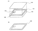
実施例5及び6で説明したIDタグの利用形態について説明する。なお、本実施例では、実施例5及び6のIDタグを搭載したカード(以下、IDFカードと表記する)を用いて説明する。
The usage mode of the ID tag described in the fifth and sixth embodiments will be described. In the present embodiment, description will be made using a card (hereinafter referred to as an IDF card) on which the ID tag of
図14(A)には、絶縁基板1401上に、識別情報を有するIDFチップ1402、アンテナ1403が設けられている。
In FIG. 14A, an
そして図14(B)に示すように、第1のフィルム1404及び第2のフィルム1405を貼り合わせ、IDFカード1406を完成させる。このときIDFチップは、実装するカードに対して中心部に配置し、IDFチップの周囲は物品の基材、本実施の形態においては第1及び第2のフィルムで覆われるように形成するとよい。その結果、IDFチップの機械的強度を高めることができる。具体的には、IDFチップを挟み込む位置(IDFチップの中心):Xは、カードの厚みをDとすると、(1/2)×D−30μm<X<(1/2)×D+30μmを満たすように配置するとするとよい。
Then, as shown in FIG. 14B, the
また本実施の形態では、基板上にアンテナが形成されたIDFチップを用いる場合で説明したが、アンテナが実装されたIDFチップを用いた場合であってもよく、IDFチップは上記位置を満たすと好ましい。 In this embodiment, the case where an IDF chip having an antenna formed on a substrate is used is described. However, an IDF chip on which an antenna is mounted may be used, and the IDF chip satisfies the above position. preferable.
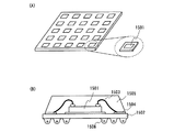
本発明の半導体記憶装置をチップ化し、特定の用途を想定した装置の内部に組み込まれる場合について図15を用いて説明する。本実施例ではBGA(ball grid array)技術によりパッケージされ実装化される例を説明する。 A case where the semiconductor memory device of the present invention is formed into a chip and incorporated in a device assuming a specific application will be described with reference to FIG. In the present embodiment, an example of packaging and mounting by BGA (ball grid array) technology will be described.
図15(A)に示すように、本発明の半導体記憶装置が複数作製された基板から切り分けられた半導体記憶装置1501は、樹脂基板等の基板1502に貼り付けられる。また、半導体記憶装置1501は、金線からなるワイヤ1503によりリードフレーム1504にワイヤボンディングされ、樹脂1505で封止されている。半導体記憶装置1501が貼り付けられている樹脂基板の反対側には、はんだボール端子1506が形成される。このようにパッケージされたチップは、はんだボール端子1506を介して特定の装置に実装される。
As shown in FIG. 15A, a
本発明の半導体記憶装置は同一基板上に作製できるため、本実施例のように半導体記憶装置を複数作製した後に切り離し、一度に大量のメモリチップを作製できる。 Since the semiconductor memory device of the present invention can be manufactured over the same substrate, a plurality of semiconductor memory devices are manufactured and then separated as in this embodiment, and a large number of memory chips can be manufactured at one time.
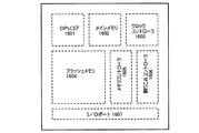
本発明の半導体記憶装置の一例である不揮発性メモリを、ワンチップ上に集積化されたシステムLSIに適用する場合について説明する。 A case where a nonvolatile memory which is an example of a semiconductor memory device of the present invention is applied to a system LSI integrated on one chip will be described.
なお、システムLSIとは、特定の用途を想定した装置の内部に組み込まれ、装置の制御やデータ処理を行うシステムを構成するLSIである。用途は多岐にわたり、例えば、携帯電話、PDA、DSC、テレビ、プリンタ、FAX、ゲーム機、カーナビゲーション、DVDプレーヤ、などを挙げることができる。 The system LSI is an LSI that is incorporated in a device that assumes a specific application and constitutes a system that controls the device and performs data processing. Applications are diverse and include, for example, mobile phones, PDAs, DSCs, televisions, printers, FAX machines, game machines, car navigation systems, DVD players, and the like.
図16に示すのは、システムLSIの一例である。システムLSIは典型的にはCPUコア1601、フラッシュメモリ1604、クロックコントローラ1603、メインメモリ1602、メモリコントローラ1605、割り込みコントローラ1606、I/Oポート1607等から構成される。もちろん、図16に示すシステムLSIは簡略化した一例であり、実際のシステムLSIはその用途によって多種多様な回路設計が行われる。
FIG. 16 shows an example of a system LSI. The system LSI typically includes a
フラッシュメモリ1604に本発明の半導体記憶装置を構成するメモリトランジスタを用いることができる。メインメモリ1602としては、例えばSRAMやDRAMを用いることができる。本発明の半導体記憶装置をシステムLSIのフラッシュメモリとすることにより、システムLSIのコストの低減及び小型化を実現できる。
A memory transistor constituting the semiconductor memory device of the present invention can be used for the
また、CPUコア1601、クロックコントローラ1603、メインメモリ1602、メモリコントローラ1605、割り込みコントローラ1606、I/Oポート1607を構成するトランジスタとして、高速動作をするトランジスタが必要な場合は、本発明の半導体記憶装置を構成する高速トランジスタの作製と同様に作製することができる。これより、同一基板上に半導体装置とともにその他の回路も効率よく作製することが可能となる。
If a transistor that operates at high speed is required as a transistor constituting the
本実施例は、実施形態1〜2、実施例1〜4と組み合わせて用いることが可能である。また、実施例8では半導体記憶装置をチップ化した例であったが、本実施例でも同様にシステムLSIをパッケージングして、実装化しても良い。 This example can be used in combination with Embodiments 1-2 and Examples 1-4. In the eighth embodiment, the semiconductor memory device is formed as a chip. However, in this embodiment, the system LSI may be packaged and mounted in the same manner.
本実施例は、パネルと同一基板上に本発明の半導体記憶装置を貼り付ける、又は作製する例を図17及び図18を用いて説明する。 In this embodiment, an example in which the semiconductor memory device of the present invention is attached or manufactured over the same substrate as the panel will be described with reference to FIGS.
図17(A)は、画素部1701と同一基板上に、本発明の半導体記憶装置が設けられた例である。基板1702はどのような基板でもよくガラス基板でも良い。1703はメモリ部、1704はゲート側駆動回路、1705はソース側駆動回路、1706は外部入力端子である。図17(A)のA−A’で切った断面図を図17(B)に示す。基板1702上には画素部1701、ゲート側駆動回路1704が形成されており、画素部1701は電流制御用薄膜トランジスタ1710とそのドレインに電気的に接続された画素電極1711を含む複数の画素により形成される。また、ゲート側駆動回路1704はnチャネル型薄膜トランジスタとpチャネル型FETとを相補的に組み合わせたCMOS回路1712を用いて形成される。
FIG. 17A illustrates an example in which the semiconductor memory device of the present invention is provided over the same substrate as the
画素電極1711はEL素子の陰極として機能する。また、画素電極1711上には発光層、正孔注入層が形成される。また、その上にはEL素子の陽極、パッシベーション膜等が形成される。メモリ部1703は、高速トランジスタ1721、高耐圧トランジスタ1722、メモリトランジスタ1723で形成される。
The
メモリ部1703と駆動回路又は画素部とは、接続配線1714を経由し、さらに異方性導電性フィルム1716、電極パッド1717を介して、電気的に接続されている。より具体的には、半導体記憶装置の高速トランジスタの配線部分が、駆動回路又は画素部と電気的に接続している。
The
1718はカバー材、1719は第1シール材、1720は第2シール材であり、第1シール材1719で囲まれた内側のカバー材1718と基板1702との間には充填材(図示せず)が設けられる。
図17(B)は、半導体記憶装置を逆さまにして基板1702に貼り付けた例だが、逆さまにせず、基板1702と半導体記憶装置が形成されている基板とを接着しても良い。また、本実施例ではEL表示装置について説明したが、液晶パネルと同一基板上に半導体記憶装置を設けて、液晶表示装置にも適用できることは言うまでもない。
FIG. 17B illustrates an example in which the semiconductor memory device is attached to the
以上より、画素部のメモリとして本発明の半導体記憶装置を設けることができ、低コストで小型のメモリを備える表示装置を提供できる。 As described above, the semiconductor memory device of the present invention can be provided as the memory of the pixel portion, and a display device including a small memory at low cost can be provided.
図18は、画素部と駆動回路が設けられている同一基板上にメモリ部を設けた場合の例である。図18において、図17と共通の部分は同じ符号を付して詳しい説明を省略する。図18において、図示されていはいないが、メモリ部の高速トランジスタの配線と周辺駆動回路は、各トランジスタのソース領域及びドレイン領域に直接接続している配線同士により、電気的に接続している。従って、図17の場合よりも、より簡単に駆動回路部とメモリ部とを接続できる。図18の構成では、全てが同一基板上に同時に作製できるため、図17で説明した構成よりもさらに小型で低コストの表示装置が得られ、作製工程も簡略化できる。 FIG. 18 illustrates an example in which the memory portion is provided over the same substrate where the pixel portion and the driver circuit are provided. 18, parts common to FIG. 17 are given the same reference numerals and detailed description thereof is omitted. In FIG. 18, although not shown, the high-speed transistor wiring and the peripheral driver circuit in the memory portion are electrically connected to each other by wiring directly connected to the source region and the drain region of each transistor. Therefore, the drive circuit portion and the memory portion can be more easily connected than in the case of FIG. In the structure of FIG. 18, since all can be manufactured on the same substrate at the same time, a display device that is smaller and less expensive than the structure described in FIG. 17 can be obtained, and the manufacturing process can be simplified.
本発明を用いて様々な半導体装置を完成させることができる。その一例は、携帯情報端末(電子手帳、モバイルコンピュータ、携帯電話など)、ビデオカメラ、デジタルカメラ、パーソナルコンピュータ、テレビ受像器、投影型表示装置などが挙げられる。それらの一例を図に示す。なお、本発明の半導体記憶装置が図19に示す装置へ実装される又は配置される方法は、実施例8〜10を参照する。 Various semiconductor devices can be completed using the present invention. Examples thereof include portable information terminals (electronic notebooks, mobile computers, mobile phones, etc.), video cameras, digital cameras, personal computers, television receivers, projection display devices, and the like. An example of them is shown in the figure. Note that Examples 8 to 10 are referred to for a method of mounting or arranging the semiconductor memory device of the present invention in the device shown in FIG.
図19(A)は本発明を適用してテレビ受像器を完成させる一例であり、筐体2401、支持台2402、表示部2403などにより構成されている。本発明の半導体記憶装置を備えることで低コストなテレビ受像器を提供できる。
FIG. 19A illustrates an example in which a television receiver is completed by applying the present invention, which includes a housing 2401, a
図19(B)は本発明を適用してビデオカメラを完成させた一例であり、本体2411、表示部2412、音声入力部2413、操作スイッチ2414、バッテリー2415、受像部2416などにより構成されている。本発明の半導体記憶装置を備えることで低コストなビデオカメラを提供できる。
FIG. 19B shows an example in which the present invention is applied to complete a video camera, which includes a main body 2411, a display portion 2412, an
図19(C)は本発明を適用してノート型のパーソナルコンピュータを完成させた一例であり、本体2421、筐体2422、表示部2423、キーボード2424などにより構成されている。本発明の半導体記憶装置を備えることで低コストなパーソナルコンピュータを提供できる。
FIG. 19C illustrates an example in which a laptop personal computer is completed by applying the present invention, which includes a
図19(D)は本発明を適用してPDA(Personal Digital Assistant)を完成させた一例であり、本体2431、スタイラス2432、表示部2433、操作ボタン2434、外部インターフェース2435などにより構成されている。本発明の半導体記憶装置を備えることで低コストなPDAを提供できる。
FIG. 19D is an example in which a PDA (Personal Digital Assistant) is completed by applying the present invention, which includes a
図19(E)は本発明を適用して音響再生装置を完成させた一例であり、具体的には車載用のオーディオ装置であり、本体2441、表示部2442、操作スイッチ2443、2444などにより構成されている。本発明の半導体記憶装置を備えることで低コストな音響再生装置を提供できる。
FIG. 19E is an example in which a sound reproducing device is completed by applying the present invention, specifically an in-vehicle audio device, which includes a
図19(F)は本発明を適用してデジタルカメラを完成させた一例であり、本体2451、表示部(A)2452、接眼部2453、操作スイッチ2454、表示部(B)2455、バッテリー2456などにより構成されている。本発明の半導体記憶装置を備えることで低コストなデジタルカメラを提供できる。
FIG. 19F illustrates an example in which the present invention is applied to complete a digital camera. A
図19(G)は本発明を適用して携帯電話を完成させた一例であり、本体2461、音声出力部2462、音声入力部2463、表示部2464、操作スイッチ2465、アンテナ2466などにより構成されている。本発明の半導体記憶装置を備えることで低コストな携帯電話を提供できる。
FIG. 19G illustrates an example of a cellular phone completed by applying the present invention, which includes a
なお、ここで示す装置はごく一例であり、これらの用途に限定するものではない。 In addition, the apparatus shown here is an example only and is not limited to these uses.
本実施例は、実施形態1〜2、実施例1〜4、8〜10と組み合わせて用いることが可能である。 This example can be used in combination with Embodiments 1-2, Examples 1-4, and 8-10.
101 基板
102 活性層
103 活性層
104 活性層
105 第1絶縁膜
106 第1導電膜
107 膜
107a 膜
108 膜
109 第2絶縁膜
110 第2導電膜
111 レジストマスク
112 レジストマスク
114 上部ゲート電極
115 ゲート電極
116 制御ゲート電極
117 パターン
118 パターン
119 下部ゲート電極
120 浮遊ゲート電極
121 層間絶縁膜
122 配線
128 配線
DESCRIPTION OF
Claims (16)
第2の活性層と、前記第2の活性層上のゲート絶縁膜と、前記ゲート絶縁膜上のゲート電極を有する第2のトランジスタと、
を同一基板上に有し、
第2のトランジスタの前記ゲート絶縁膜は下部ゲート絶縁膜と上部ゲート絶縁膜を有し、
第2のトランジスタの前記下部ゲート絶縁膜は前記第1ゲート絶縁膜と同じ層から形成され、前記上部ゲート絶縁膜は前記第2ゲート絶縁膜と同じ層から形成されていることを特徴とする半導体装置。 A first active layer; a first gate insulating film on the first active layer; a floating gate electrode on the first gate insulating film; a second gate insulating film on the floating gate electrode; A first transistor having a control gate electrode on a two-gate insulating film;
A second transistor having a second active layer, a gate insulating film on the second active layer, and a gate electrode on the gate insulating film;
On the same substrate,
The gate insulating film of the second transistor has a lower gate insulating film and an upper gate insulating film;
The lower gate insulating film of the second transistor is formed from the same layer as the first gate insulating film, and the upper gate insulating film is formed from the same layer as the second gate insulating film. apparatus.
第2の活性層と、前記第2の活性層上のゲート絶縁膜と、前記ゲート絶縁膜上のゲート電極とを有する第2のトランジスタと、
を同一基板上に有し、
第2トランジスタの前記ゲート電極は下部ゲート電極と上部ゲート電極とを有し、
第2のトランジスタの前記下部ゲート電極は前記浮遊ゲート電極と同じ層から形成され、前記上部ゲート電極は前記制御ゲート電極と同じ層から形成されていることを特徴とする半導体装置。 A first active layer; a first gate insulating film on the first active layer; a floating gate electrode on the first gate insulating film; a second gate insulating film on the floating gate electrode; A first transistor having a control gate electrode on a two-gate insulating film;
A second transistor having a second active layer, a gate insulating film on the second active layer, and a gate electrode on the gate insulating film;
On the same substrate,
The gate electrode of the second transistor has a lower gate electrode and an upper gate electrode;
The semiconductor device, wherein the lower gate electrode of the second transistor is formed from the same layer as the floating gate electrode, and the upper gate electrode is formed from the same layer as the control gate electrode.
第2の活性層と、前記第2の活性層上のゲート絶縁膜と、前記ゲート絶縁膜上のゲート電極とを有する第2のトランジスタと、
第3の活性層と、前記第3の活性層上のゲート絶縁膜と、前記ゲート絶縁膜上のゲート電極を有する第3のトランジスタと、
を同一基板上に有し、
第3のトランジスタの前記ゲート絶縁膜は下部ゲート絶縁膜と上部ゲート絶縁膜を有し、
第3のトランジスタの前記下部ゲート絶縁膜は前記第1ゲート絶縁膜及び第2のトランジスタの前記ゲート絶縁膜と同じ層から形成され、前記上部ゲート絶縁膜は前記第2ゲート絶縁膜と同じ層から形成されており、
第2のトランジスタの前記ゲート電極は下部ゲート電極と上部ゲート電極を有し、
第2のトランジスタの前記下部ゲート電極は前記浮遊ゲート電極と同じ層から形成され、前記上部ゲート電極は前記制御ゲート電極及び第3のトランジスタの前記ゲート電極と同じ層から形成されていることを特徴とする半導体装置。 A first active layer; a first gate insulating film on the first active layer; a floating gate electrode on the first gate insulating film; a second gate insulating film on the floating gate electrode; A first transistor having a control gate electrode on a two-gate insulating film;
A second transistor having a second active layer, a gate insulating film on the second active layer, and a gate electrode on the gate insulating film;
A third transistor having a third active layer, a gate insulating film on the third active layer, and a gate electrode on the gate insulating film;
On the same substrate,
The gate insulating film of the third transistor has a lower gate insulating film and an upper gate insulating film;
The lower gate insulating film of the third transistor is formed from the same layer as the first gate insulating film and the gate insulating film of the second transistor, and the upper gate insulating film is formed from the same layer as the second gate insulating film. Formed,
The gate electrode of the second transistor has a lower gate electrode and an upper gate electrode;
The lower gate electrode of the second transistor is formed from the same layer as the floating gate electrode, and the upper gate electrode is formed from the same layer as the control gate electrode and the gate electrode of the third transistor. A semiconductor device.
前記第1絶縁膜上に第1導電膜を形成し、
前記第1導電膜を選択的にエッチングすることにより、前記第2のトランジスタの活性層上の前記第1導電膜を除去して、前記第2のトランジスタの活性層上の前記第1絶縁膜を露出させ、
前記エッチングされた第1導電膜及び前記露出した第1絶縁膜上に第2絶縁膜を形成し、
前記第2絶縁膜上に第2導電膜を形成し、
前記第2導電膜をエッチングすることにより、第2のトランジスタのゲート電極及び第1のトランジスタの制御ゲート電極を形成し、
前記第2導電膜のエッチングの後、前記第2絶縁膜をエッチングし、
前記第2絶縁膜のエッチングの後、前記エッチングされた第1導電膜をエッチングすることにより、第2のトランジスタの浮遊ゲート電極を形成し、
第2のトランジスタのゲート絶縁膜は前記第1絶縁膜及び前記第2絶縁膜からなり、
第1のトランジスタと第2のトランジスタは同一基板上に設けられていることを特徴とする半導体装置の作製方法。 Forming a first insulating film on the active layer of the first transistor and the active layer of the second transistor;
Forming a first conductive film on the first insulating film;
The first conductive film on the active layer of the second transistor is removed by selectively etching the first conductive film, and the first insulating film on the active layer of the second transistor is removed. To expose
Forming a second insulating film on the etched first conductive film and the exposed first insulating film;
Forming a second conductive film on the second insulating film;
Etching the second conductive film forms a gate electrode of the second transistor and a control gate electrode of the first transistor,
After etching the second conductive film, the second insulating film is etched,
After the etching of the second insulating film, the etched first conductive film is etched to form a floating gate electrode of the second transistor,
The gate insulating film of the second transistor is composed of the first insulating film and the second insulating film,
A method for manufacturing a semiconductor device, wherein the first transistor and the second transistor are provided over the same substrate.
前記第1絶縁膜上に第1導電膜を形成し、
前記第1導電膜上に第2絶縁膜を形成し、
前記第2絶縁膜を選択的にエッチングすることにより、前記第2のトランジスタの活性層上の前記第2絶縁膜を除去して、前記第2のトランジスタの活性層上の第1導電膜を露出させ、
前記エッチングされた第2絶縁膜及び前記露出された第1導電膜上に、第2導電膜を形成し、
前記第2導電膜をエッチングすることにより、第2のトランジスタの上部ゲート電極と第1のトランジスタの制御ゲート電極を形成し、
前記第1導電膜をエッチングすることにより、第2のトランジスタの下部ゲート電極と第1のトランジスタの浮遊ゲート電極を形成し、
第1のトランジスタと第2のトランジスタは同一基板上に設けられていることを特徴とする半導体装置の作製方法。 Forming a first insulating film on the active layer of the first transistor and the active layer of the second transistor;
Forming a first conductive film on the first insulating film;
Forming a second insulating film on the first conductive film;
By selectively etching the second insulating film, the second insulating film on the active layer of the second transistor is removed, and the first conductive film on the active layer of the second transistor is exposed. Let
Forming a second conductive film on the etched second insulating film and the exposed first conductive film;
Etching the second conductive film forms an upper gate electrode of the second transistor and a control gate electrode of the first transistor,
Etching the first conductive film forms a lower gate electrode of the second transistor and a floating gate electrode of the first transistor,
A method for manufacturing a semiconductor device, wherein the first transistor and the second transistor are provided over the same substrate.
前記第1絶縁膜上に第1導電膜を形成し、
前記第1導電膜に選択的に第1のエッチングをすることにより、前記第3のトランジスタの活性層上の前記第1導電膜を除去して、前記第3のトランジスタの活性層上の第1絶縁膜を露出させ、
前記第1のエッチングをされた第1導電膜及び前記露出した第1絶縁膜上に、第2絶縁膜を形成し、
前記第2絶縁膜に選択的に第2のエッチングをすることにより、前記第2のトランジスタの活性層上の前記第2絶縁膜を除去して、前記第2のトランジスタの活性層上の第1導電膜を露出させ、
前記第2のエッチングをされた第2絶縁膜及び前記露出した第1導電膜上に、第2導電膜を形成し、
前記第2導電膜に第3のエッチングをすることにより、第1のトランジスタの制御ゲート電極、第2のトランジスタの上部ゲート電極及び第3のトランジスタのゲート電極及びを形成し、
前記第2のエッチングをされた第2絶縁膜に第4のエッチングをし、
前記第1のエッチングをされた第1導電膜に第5のエッチングをすることにより、第1のトランジスタの浮遊ゲート電極及び第2のトランジスタの下部ゲート電極を形成し、
第3のトランジスタのゲート絶縁膜は前記第1絶縁膜及び前記第2絶縁膜からなり、
第1のトランジスタ、第2のトランジスタ及び第3のトランジスタは同一基板上に設けられることを特徴とする半導体装置の作製方法。 Forming a first insulating film on the active layer of the first transistor, the active layer of the second transistor, and the active layer of the third transistor;
Forming a first conductive film on the first insulating film;
The first conductive film on the active layer of the third transistor is removed by selectively performing the first etching on the first conductive film, and the first conductive film on the active layer of the third transistor is removed. Exposing the insulation film,
Forming a second insulating film on the first etched conductive film and the exposed first insulating film;
By selectively performing a second etching on the second insulating film, the second insulating film on the active layer of the second transistor is removed, and a first on the active layer of the second transistor is removed. Exposing the conductive film,
Forming a second conductive layer on the second etched second insulating layer and the exposed first conductive layer;
A third etching is performed on the second conductive film to form a control gate electrode of the first transistor, an upper gate electrode of the second transistor, and a gate electrode of the third transistor,
Performing a fourth etching on the second insulating film subjected to the second etching;
Forming a floating gate electrode of the first transistor and a lower gate electrode of the second transistor by performing a fifth etching on the first conductive film subjected to the first etching;
The gate insulating film of the third transistor is composed of the first insulating film and the second insulating film,
A method for manufacturing a semiconductor device, wherein the first transistor, the second transistor, and the third transistor are provided over the same substrate.
16. The method for manufacturing a semiconductor device according to claim 9, wherein the substrate is a semiconductor substrate, a quartz substrate, a glass substrate, or a plastic substrate.
Priority Applications (1)
| Application Number | Priority Date | Filing Date | Title |
|---|---|---|---|
| JP2005061959A JP4896416B2 (en) | 2004-03-08 | 2005-03-07 | Method for manufacturing semiconductor device |
Applications Claiming Priority (3)
| Application Number | Priority Date | Filing Date | Title |
|---|---|---|---|
| JP2004063901 | 2004-03-08 | ||
| JP2004063901 | 2004-03-08 | ||
| JP2005061959A JP4896416B2 (en) | 2004-03-08 | 2005-03-07 | Method for manufacturing semiconductor device |
Publications (3)
| Publication Number | Publication Date |
|---|---|
| JP2005294814A true JP2005294814A (en) | 2005-10-20 |
| JP2005294814A5 JP2005294814A5 (en) | 2008-03-27 |
| JP4896416B2 JP4896416B2 (en) | 2012-03-14 |
Family
ID=35327350
Family Applications (1)
| Application Number | Title | Priority Date | Filing Date |
|---|---|---|---|
| JP2005061959A Expired - Fee Related JP4896416B2 (en) | 2004-03-08 | 2005-03-07 | Method for manufacturing semiconductor device |
Country Status (1)
| Country | Link |
|---|---|
| JP (1) | JP4896416B2 (en) |
Cited By (11)
| Publication number | Priority date | Publication date | Assignee | Title |
|---|---|---|---|---|
| WO2007077850A1 (en) * | 2005-12-27 | 2007-07-12 | Semiconductor Energy Laboratory Co., Ltd. | Semiconductor device and manufacturing method thereof |
| JP2007288177A (en) * | 2006-03-21 | 2007-11-01 | Semiconductor Energy Lab Co Ltd | Nonvolatile semiconductor memory device |
| JP2007288176A (en) * | 2006-03-21 | 2007-11-01 | Semiconductor Energy Lab Co Ltd | Nonvolatile semiconductor memory device |
| JP2007294910A (en) * | 2006-03-31 | 2007-11-08 | Semiconductor Energy Lab Co Ltd | Nonvolatile semiconductor memory device |
| JP2007294911A (en) * | 2006-03-31 | 2007-11-08 | Semiconductor Energy Lab Co Ltd | Nonvolatile semiconductor memory device |
| WO2007138754A1 (en) * | 2006-05-31 | 2007-12-06 | Sharp Kabushiki Kaisha | Semiconductor device, method for manufacturing same, and display |
| JP2007324561A (en) * | 2006-06-02 | 2007-12-13 | Hynix Semiconductor Inc | Integrated circuit and information recording method |
| US7745827B2 (en) | 2005-09-29 | 2010-06-29 | Semiconductor Energy Laboratory Co., Ltd. | Memory device |
| JP2013051425A (en) * | 2006-03-31 | 2013-03-14 | Semiconductor Energy Lab Co Ltd | Semiconductor device |
| US8581260B2 (en) | 2007-02-22 | 2013-11-12 | Semiconductor Energy Laboratory Co., Ltd. | Semiconductor device including a memory |
| KR101345418B1 (en) * | 2006-03-21 | 2013-12-24 | 가부시키가이샤 한도오따이 에네루기 켄큐쇼 | Nonvolatile semiconductor memory device |
Citations (4)
| Publication number | Priority date | Publication date | Assignee | Title |
|---|---|---|---|---|
| JPH09148458A (en) * | 1995-11-08 | 1997-06-06 | Lg Semicon Co Ltd | Manufacture of semiconductor element with floating gate |
| JPH1187545A (en) * | 1997-07-08 | 1999-03-30 | Sony Corp | Semiconductor nonvolatile memory device and method of manufacturing the same |
| JP2003518742A (en) * | 1999-12-21 | 2003-06-10 | コーニンクレッカ フィリップス エレクトロニクス エヌ ヴィ | Non-volatile memory cells and peripherals |
| JP2003249579A (en) * | 2003-02-10 | 2003-09-05 | Toshiba Corp | Nonvolatile semiconductor memory device and method of manufacturing the same |
-
2005
- 2005-03-07 JP JP2005061959A patent/JP4896416B2/en not_active Expired - Fee Related
Patent Citations (4)
| Publication number | Priority date | Publication date | Assignee | Title |
|---|---|---|---|---|
| JPH09148458A (en) * | 1995-11-08 | 1997-06-06 | Lg Semicon Co Ltd | Manufacture of semiconductor element with floating gate |
| JPH1187545A (en) * | 1997-07-08 | 1999-03-30 | Sony Corp | Semiconductor nonvolatile memory device and method of manufacturing the same |
| JP2003518742A (en) * | 1999-12-21 | 2003-06-10 | コーニンクレッカ フィリップス エレクトロニクス エヌ ヴィ | Non-volatile memory cells and peripherals |
| JP2003249579A (en) * | 2003-02-10 | 2003-09-05 | Toshiba Corp | Nonvolatile semiconductor memory device and method of manufacturing the same |
Cited By (19)
| Publication number | Priority date | Publication date | Assignee | Title |
|---|---|---|---|---|
| US7745827B2 (en) | 2005-09-29 | 2010-06-29 | Semiconductor Energy Laboratory Co., Ltd. | Memory device |
| US8476632B2 (en) | 2005-12-27 | 2013-07-02 | Semiconductor Energy Laboratory Co., Ltd. | Semiconductor device and manufacturing method thereof |
| WO2007077850A1 (en) * | 2005-12-27 | 2007-07-12 | Semiconductor Energy Laboratory Co., Ltd. | Semiconductor device and manufacturing method thereof |
| US9177242B2 (en) | 2005-12-27 | 2015-11-03 | Semiconductor Energy Laboratory Co., Ltd. | Semiconductor device and manufacturing method thereof |
| EP1966740A4 (en) * | 2005-12-27 | 2014-08-27 | Semiconductor Energy Lab | SEMICONDUCTOR DEVICE AND METHOD FOR MANUFACTURING THE SAME |
| JP2010056566A (en) * | 2005-12-27 | 2010-03-11 | Semiconductor Energy Lab Co Ltd | Semiconductor device, and ic card with display function |
| JP2007200291A (en) * | 2005-12-27 | 2007-08-09 | Semiconductor Energy Lab Co Ltd | Semiconductor device and manufacturing method thereof |
| KR101233639B1 (en) | 2005-12-27 | 2013-02-15 | 가부시키가이샤 한도오따이 에네루기 켄큐쇼 | Semiconductor device and manufacturing method thereof |
| JP2007288176A (en) * | 2006-03-21 | 2007-11-01 | Semiconductor Energy Lab Co Ltd | Nonvolatile semiconductor memory device |
| US8729620B2 (en) | 2006-03-21 | 2014-05-20 | Semiconductor Energy Laboratory Co., Ltd. | Nonvolatile semiconductor memory device |
| KR101345418B1 (en) * | 2006-03-21 | 2013-12-24 | 가부시키가이샤 한도오따이 에네루기 켄큐쇼 | Nonvolatile semiconductor memory device |
| JP2007288177A (en) * | 2006-03-21 | 2007-11-01 | Semiconductor Energy Lab Co Ltd | Nonvolatile semiconductor memory device |
| JP2013051425A (en) * | 2006-03-31 | 2013-03-14 | Semiconductor Energy Lab Co Ltd | Semiconductor device |
| US8629490B2 (en) | 2006-03-31 | 2014-01-14 | Semiconductor Energy Laboratory Co., Ltd. | Nonvolatile semiconductor storage device with floating gate electrode and control gate electrode |
| JP2007294911A (en) * | 2006-03-31 | 2007-11-08 | Semiconductor Energy Lab Co Ltd | Nonvolatile semiconductor memory device |
| JP2007294910A (en) * | 2006-03-31 | 2007-11-08 | Semiconductor Energy Lab Co Ltd | Nonvolatile semiconductor memory device |
| WO2007138754A1 (en) * | 2006-05-31 | 2007-12-06 | Sharp Kabushiki Kaisha | Semiconductor device, method for manufacturing same, and display |
| JP2007324561A (en) * | 2006-06-02 | 2007-12-13 | Hynix Semiconductor Inc | Integrated circuit and information recording method |
| US8581260B2 (en) | 2007-02-22 | 2013-11-12 | Semiconductor Energy Laboratory Co., Ltd. | Semiconductor device including a memory |
Also Published As
| Publication number | Publication date |
|---|---|
| JP4896416B2 (en) | 2012-03-14 |
Similar Documents
| Publication | Publication Date | Title |
|---|---|---|
| US10896931B1 (en) | 3D semiconductor device and structure | |
| CN1691337B (en) | Semiconductor device and method for manufacturing same | |
| US7972935B2 (en) | Method for manufacturing semiconductor device | |
| US7709883B2 (en) | Nonvolatile semiconductor memory device | |
| JP5604492B2 (en) | Semiconductor device | |
| US7846817B2 (en) | Method for manufacturing semiconductor device | |
| JP4896416B2 (en) | Method for manufacturing semiconductor device | |
| KR20030078075A (en) | Programmable memory address and decode circuits with ultra thin vertical body transistors | |
| US20180331073A1 (en) | 3d semiconductor device and structure | |
| US8569170B2 (en) | Manufacturing method of semiconductor device comprising silicide layer with varied thickness | |
| US11462586B1 (en) | Method to produce 3D semiconductor devices and structures with memory | |
| KR101781482B1 (en) | Anti-fuse device, a semiconductor device comprising the same, and a system comprising the same | |
| US12015026B2 (en) | Methods of forming circuit-protection devices | |
| JP4839904B2 (en) | Semiconductor device, integrated circuit, and electronic device | |
| US20220130905A1 (en) | 3d semiconductor device and structure with transistors | |
| US9391085B2 (en) | Self-aligned split gate flash memory having liner-separated spacers above the memory gate | |
| US10290682B2 (en) | 3D IC semiconductor device and structure with stacked memory | |
| CN1832176B (en) | Semiconductor device and method of operating the same | |
| US11257867B1 (en) | 3D semiconductor device and structure with oxide bonds | |
| JP2007250862A (en) | Semiconductor device, integrated circuit, and electronic device | |
| US11469271B2 (en) | Method to produce 3D semiconductor devices and structures with memory | |
| US10825864B2 (en) | 3D semiconductor device and structure | |
| JP2007294915A (en) | Nonvolatile semiconductor memory device and manufacturing method thereof | |
| JP2008177327A (en) | Semiconductor device and manufacturing method thereof |
Legal Events
| Date | Code | Title | Description |
|---|---|---|---|
| A521 | Request for written amendment filed |
Free format text: JAPANESE INTERMEDIATE CODE: A523 Effective date: 20080212 |
|
| A621 | Written request for application examination |
Free format text: JAPANESE INTERMEDIATE CODE: A621 Effective date: 20080212 |
|
| A977 | Report on retrieval |
Free format text: JAPANESE INTERMEDIATE CODE: A971007 Effective date: 20100831 |
|
| A131 | Notification of reasons for refusal |
Free format text: JAPANESE INTERMEDIATE CODE: A131 Effective date: 20110913 |
|
| A521 | Request for written amendment filed |
Free format text: JAPANESE INTERMEDIATE CODE: A523 Effective date: 20111020 |
|
| TRDD | Decision of grant or rejection written | ||
| A01 | Written decision to grant a patent or to grant a registration (utility model) |
Free format text: JAPANESE INTERMEDIATE CODE: A01 Effective date: 20111220 |
|
| A01 | Written decision to grant a patent or to grant a registration (utility model) |
Free format text: JAPANESE INTERMEDIATE CODE: A01 |
|
| A61 | First payment of annual fees (during grant procedure) |
Free format text: JAPANESE INTERMEDIATE CODE: A61 Effective date: 20111221 |
|
| R150 | Certificate of patent or registration of utility model |
Free format text: JAPANESE INTERMEDIATE CODE: R150 |
|
| FPAY | Renewal fee payment (event date is renewal date of database) |
Free format text: PAYMENT UNTIL: 20150106 Year of fee payment: 3 |
|
| FPAY | Renewal fee payment (event date is renewal date of database) |
Free format text: PAYMENT UNTIL: 20150106 Year of fee payment: 3 |
|
| R250 | Receipt of annual fees |
Free format text: JAPANESE INTERMEDIATE CODE: R250 |
|
| R250 | Receipt of annual fees |
Free format text: JAPANESE INTERMEDIATE CODE: R250 |
|
| R250 | Receipt of annual fees |
Free format text: JAPANESE INTERMEDIATE CODE: R250 |
|
| LAPS | Cancellation because of no payment of annual fees |