JP2005294615A - 配線基板 - Google Patents
配線基板 Download PDFInfo
- Publication number
- JP2005294615A JP2005294615A JP2004108828A JP2004108828A JP2005294615A JP 2005294615 A JP2005294615 A JP 2005294615A JP 2004108828 A JP2004108828 A JP 2004108828A JP 2004108828 A JP2004108828 A JP 2004108828A JP 2005294615 A JP2005294615 A JP 2005294615A
- Authority
- JP
- Japan
- Prior art keywords
- wiring
- wiring layer
- bonding
- fpc
- bumps
- Prior art date
- Legal status (The legal status is an assumption and is not a legal conclusion. Google has not performed a legal analysis and makes no representation as to the accuracy of the status listed.)
- Pending
Links
Images

Classifications
-
- H—ELECTRICITY
- H10—SEMICONDUCTOR DEVICES; ELECTRIC SOLID-STATE DEVICES NOT OTHERWISE PROVIDED FOR
- H10W—GENERIC PACKAGES, INTERCONNECTIONS, CONNECTORS OR OTHER CONSTRUCTIONAL DETAILS OF DEVICES COVERED BY CLASS H10
- H10W90/00—Package configurations
- H10W90/701—Package configurations characterised by the relative positions of pads or connectors relative to package parts
- H10W90/721—Package configurations characterised by the relative positions of pads or connectors relative to package parts of bump connectors
- H10W90/724—Package configurations characterised by the relative positions of pads or connectors relative to package parts of bump connectors between a chip and a stacked insulating package substrate, interposer or RDL
Landscapes
- Production Of Multi-Layered Print Wiring Board (AREA)
- Structure Of Printed Boards (AREA)
- Wire Bonding (AREA)
Abstract
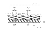
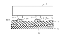
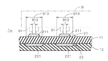
【解決手段】FPC1において、電子部品9のバンプ91が接合される電極211と重なるように、電極211を有する配線層21とは別の配線層22に対向部221を設ける。これにより、電子部品9をFPC1に押圧して実装する際に、各電極211が水平姿勢のまま同様に押し込まれ、各バンプ91が電極211に同様の力で押圧され、接合信頼性を向上することができる。
【選択図】図1
Description
9 電子部品
11〜13 絶縁層
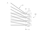
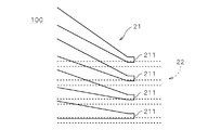
21〜24,28 配線層
91 バンプ
211 電極
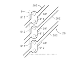
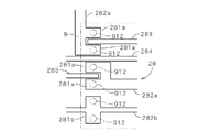
221,241,281a,281b 対向部
282,282a,282b 配線
911 接合中心
912 接合領域
Claims (6)
- 可撓性を有する配線基板であって、
複数の配線層と、
前記複数の配線層の間に設けられた少なくとも1つの絶縁層と、
を備え、
前記複数の配線層のうちの表面に露出する一の配線層が、加圧を伴う接合により電子部品の複数のバンプがそれぞれ接合される複数の電極を備え、
前記複数の配線層のうちの他の一の配線層のパターンが、前記複数のバンプのそれぞれの接合中心と重なることを特徴とする配線基板。 - 請求項1に記載の配線基板であって、
前記他の一の配線層のパターンのうち前記複数のバンプの接合中心に重なる部位が、配線に含まれることを特徴とする配線基板。 - 請求項2に記載の配線基板であって、
前記他の一の配線層のパターンのうち前記複数のバンプの接合中心に重なる部位が、複数の配線に含まれることを特徴とする配線基板。 - 請求項1ないし3のいずれかに記載の配線基板であって、
前記他の一の配線層のパターンが、前記複数のバンプのそれぞれの接合領域全体と重なることを特徴とする配線基板。 - 請求項4に記載の配線基板であって、
前記他の一の配線層のパターンが、前記複数のバンプのそれぞれの接合領域を、バンプの接合誤差および前記一の配線層と前記他の一の配線層との間の誤差の分だけ拡大した領域全体と重なることを特徴とする配線基板。 - 請求項1ないし5のいずれかに記載の配線基板であって、
前記他の一の配線層が、前記一の配線層側から2番目の配線層または前記一の配線層が形成された露出面とは反対側の露出面上に形成された配線層であることを特徴とする配線基板。
Priority Applications (1)
| Application Number | Priority Date | Filing Date | Title |
|---|---|---|---|
| JP2004108828A JP2005294615A (ja) | 2004-04-01 | 2004-04-01 | 配線基板 |
Applications Claiming Priority (1)
| Application Number | Priority Date | Filing Date | Title |
|---|---|---|---|
| JP2004108828A JP2005294615A (ja) | 2004-04-01 | 2004-04-01 | 配線基板 |
Publications (1)
| Publication Number | Publication Date |
|---|---|
| JP2005294615A true JP2005294615A (ja) | 2005-10-20 |
Family
ID=35327196
Family Applications (1)
| Application Number | Title | Priority Date | Filing Date |
|---|---|---|---|
| JP2004108828A Pending JP2005294615A (ja) | 2004-04-01 | 2004-04-01 | 配線基板 |
Country Status (1)
| Country | Link |
|---|---|
| JP (1) | JP2005294615A (ja) |
Cited By (4)
| Publication number | Priority date | Publication date | Assignee | Title |
|---|---|---|---|---|
| JP2008164427A (ja) * | 2006-12-28 | 2008-07-17 | Micronics Japan Co Ltd | プローブユニット基板 |
| WO2009022522A1 (ja) * | 2007-08-10 | 2009-02-19 | Sharp Kabushiki Kaisha | 配線基板、及び、液晶表示装置 |
| US8310645B2 (en) | 2008-06-25 | 2012-11-13 | Sharp Kabushiki Kaisha | Wiring board and liquid crystal display device |
| JP2013065810A (ja) * | 2011-08-31 | 2013-04-11 | Denso Corp | 多層基板 |
-
2004
- 2004-04-01 JP JP2004108828A patent/JP2005294615A/ja active Pending
Cited By (5)
| Publication number | Priority date | Publication date | Assignee | Title |
|---|---|---|---|---|
| JP2008164427A (ja) * | 2006-12-28 | 2008-07-17 | Micronics Japan Co Ltd | プローブユニット基板 |
| WO2009022522A1 (ja) * | 2007-08-10 | 2009-02-19 | Sharp Kabushiki Kaisha | 配線基板、及び、液晶表示装置 |
| US8319932B2 (en) | 2007-08-10 | 2012-11-27 | Sharp Kabushiki Kaisha | Wiring board and liquid crystal display device |
| US8310645B2 (en) | 2008-06-25 | 2012-11-13 | Sharp Kabushiki Kaisha | Wiring board and liquid crystal display device |
| JP2013065810A (ja) * | 2011-08-31 | 2013-04-11 | Denso Corp | 多層基板 |
Similar Documents
| Publication | Publication Date | Title |
|---|---|---|
| JP2664873B2 (ja) | 電子パッケージおよびその作製方法 | |
| JP2004343030A (ja) | 配線回路基板とその製造方法とその配線回路基板を備えた回路モジュール | |
| EP1005086A2 (en) | Metal foil having bumps, circuit substrate having the metal foil, and semiconductor device having the circuit substrate | |
| JP2004179232A (ja) | 半導体装置及びその製造方法並びに電子機器 | |
| CN1312764C (zh) | 电子元件装置及其制造方法 | |
| JP4813255B2 (ja) | 配線基板及びその製造方法ならびに半導体装置 | |
| JP2001223243A (ja) | 半導体装置及びその製造方法、回路基板並びに電子機器 | |
| JP2005294615A (ja) | 配線基板 | |
| JP2002290028A (ja) | プリント配線基板の接続方法及び接続構造 | |
| JP3438583B2 (ja) | 異方導電性フィルムの接続方法 | |
| JP2002261416A (ja) | 電極の接続構造 | |
| JP2000022329A (ja) | 配線基板および電子ユニットおよび電子部品実装方法 | |
| JP5277754B2 (ja) | フリップ接続実装体、フリップ接続実装体の製造方法 | |
| CN208128619U (zh) | 树脂基板以及部件安装树脂基板 | |
| KR100516815B1 (ko) | 반도체장치 | |
| JP2821070B2 (ja) | 複合プリント基板の接合方法 | |
| JP7351552B2 (ja) | 基板、基板製造方法及び基板接続方法 | |
| JP3627895B2 (ja) | 配線板 | |
| JP4520052B2 (ja) | 半導体装置およびその製造方法 | |
| JP4619104B2 (ja) | 半導体装置 | |
| JP4430419B2 (ja) | 平行導電回路シートを用いた電子回路及びその製造方法 | |
| CN100499054C (zh) | 半导体装置及其制造方法 | |
| JP4342577B2 (ja) | 半導体チップの実装構造 | |
| JP2002057416A (ja) | 両面接続用フレキシブル配線板 | |
| JP2009278050A (ja) | 電子モジュール、配線板、電子モジュールの製造方法、配線板の製造方法 |
Legal Events
| Date | Code | Title | Description |
|---|---|---|---|
| A621 | Written request for application examination |
Free format text: JAPANESE INTERMEDIATE CODE: A621 Effective date: 20061128 |
|
| RD01 | Notification of change of attorney |
Free format text: JAPANESE INTERMEDIATE CODE: A7421 Effective date: 20061213 |
|
| A977 | Report on retrieval |
Free format text: JAPANESE INTERMEDIATE CODE: A971007 Effective date: 20090120 |
|
| A131 | Notification of reasons for refusal |
Free format text: JAPANESE INTERMEDIATE CODE: A131 Effective date: 20090217 |
|
| A521 | Request for written amendment filed |
Free format text: JAPANESE INTERMEDIATE CODE: A523 Effective date: 20090416 |
|
| A02 | Decision of refusal |
Free format text: JAPANESE INTERMEDIATE CODE: A02 Effective date: 20090825 |