JP2005294615A - Wiring board - Google Patents
Wiring board Download PDFInfo
- Publication number
- JP2005294615A JP2005294615A JP2004108828A JP2004108828A JP2005294615A JP 2005294615 A JP2005294615 A JP 2005294615A JP 2004108828 A JP2004108828 A JP 2004108828A JP 2004108828 A JP2004108828 A JP 2004108828A JP 2005294615 A JP2005294615 A JP 2005294615A
- Authority
- JP
- Japan
- Prior art keywords
- wiring
- wiring layer
- bonding
- fpc
- bumps
- Prior art date
- Legal status (The legal status is an assumption and is not a legal conclusion. Google has not performed a legal analysis and makes no representation as to the accuracy of the status listed.)
- Pending
Links
Images

Classifications
-
- H—ELECTRICITY
- H10—SEMICONDUCTOR DEVICES; ELECTRIC SOLID-STATE DEVICES NOT OTHERWISE PROVIDED FOR
- H10W—GENERIC PACKAGES, INTERCONNECTIONS, CONNECTORS OR OTHER CONSTRUCTIONAL DETAILS OF DEVICES COVERED BY CLASS H10
- H10W90/00—Package configurations
- H10W90/701—Package configurations characterised by the relative positions of pads or connectors relative to package parts
- H10W90/721—Package configurations characterised by the relative positions of pads or connectors relative to package parts of bump connectors
- H10W90/724—Package configurations characterised by the relative positions of pads or connectors relative to package parts of bump connectors between a chip and a stacked insulating package substrate, interposer or RDL
Landscapes
- Production Of Multi-Layered Print Wiring Board (AREA)
- Structure Of Printed Boards (AREA)
- Wire Bonding (AREA)
Abstract
【課題】バンプを介してFPCに電子部品を実装する際に、補強板を用いることなく接合信頼性を向上する。
【解決手段】FPC1において、電子部品9のバンプ91が接合される電極211と重なるように、電極211を有する配線層21とは別の配線層22に対向部221を設ける。これにより、電子部品9をFPC1に押圧して実装する際に、各電極211が水平姿勢のまま同様に押し込まれ、各バンプ91が電極211に同様の力で押圧され、接合信頼性を向上することができる。
【選択図】図1When mounting an electronic component on an FPC via a bump, bonding reliability is improved without using a reinforcing plate.
In an FPC, a facing portion is provided in a wiring layer different from a wiring layer having an electrode so that bumps of an electronic component are overlapped with an electrode to be bonded. Thereby, when the electronic component 9 is pressed and mounted on the FPC 1, each electrode 211 is similarly pushed in a horizontal posture, and each bump 91 is pressed against the electrode 211 with the same force, thereby improving the bonding reliability. be able to.
[Selection] Figure 1
Description
本発明は、電子部品が実装される可撓性を有する配線基板に関する。 The present invention relates to a flexible wiring board on which electronic components are mounted.
従来より、回路基板の製造において、半導体のベアチップ上に形成された電気回路の電極上にバンプを形成し、配線基板上の電極にバンプを押圧して接合することによりベアチップを配線基板に実装する、フリップチップ接合と呼ばれる方法が利用されている。この方法において配線基板として可撓性を有するプリント基板(Flexible Printed Circuit、以下、「FPC」という。)が用いられる場合、接合時にFPC上の電極がバンプから一定の力を受けるようにするために、例えば、特許文献1に開示されているように、FPCの裏面に補強板が設けられる。
Conventionally, in manufacturing a circuit board, bumps are formed on the electrodes of an electric circuit formed on a semiconductor bare chip, and the bumps are pressed and bonded to the electrodes on the wiring board to mount the bare chip on the wiring board. A method called flip chip bonding is used. In this method, when a flexible printed circuit (hereinafter referred to as “FPC”) is used as a wiring substrate, the electrodes on the FPC receive a certain force from the bumps during bonding. For example, as disclosed in
なお、特許文献2には、ワイヤボンディング法によりICをFPCに搭載する際に裏面のパターンによりボンディング位置を補強する技術が開示されており、特許文献3には、LEDをワイヤボンディング法によりFPCに実装する場合において、配線パターンに連続する裏パターンにより、表パターンのワイヤボンディングが行われるランドパターンの裏面領域を平坦とし、これにより、裏面に補強板を取り付ける際に気泡が残存しないようにする技術が開示されている。
ところで、既述のようにフリップチップ接合の際に、補強板をFPCの裏面に貼り付ける場合、回路基板が厚くなってしまい、さらに、裏面において電子部品の実装可能な領域が減少してしまう。逆に、補強板を設けない場合は、FPCの他の層の配線パターンの影響を受けて、接合時にバンプと接触するFPC上の電極の高さや姿勢が一定とならず、接合不良が生じるおそれがある。そこで、本発明は、フリップチップ接合などのようにバンプを介して電子部品が可撓性を有する配線基板に押圧されて実装される場合に、裏面に補強板を設けることなく、接合信頼性を向上することを目的としている。 By the way, as described above, when the reinforcing plate is attached to the back surface of the FPC at the time of flip chip bonding, the circuit board becomes thick, and further, the area where electronic components can be mounted is reduced on the back surface. On the contrary, when the reinforcing plate is not provided, the height and posture of the electrode on the FPC that comes into contact with the bump at the time of bonding may not be constant due to the influence of the wiring pattern of other layers of the FPC, which may cause bonding failure. There is. Therefore, the present invention provides bonding reliability without providing a reinforcing plate on the back surface when an electronic component is pressed and mounted on a flexible wiring board through bumps such as flip chip bonding. It aims to improve.
請求項1に記載の発明は、可撓性を有する配線基板であって、複数の配線層と、前記複数の配線層の間に設けられた少なくとも1つの絶縁層とを備え、前記複数の配線層のうちの表面に露出する一の配線層が、加圧を伴う接合により電子部品の複数のバンプがそれぞれ接合される複数の電極を備え、前記複数の配線層のうちの他の一の配線層のパターンが、前記複数のバンプのそれぞれの接合中心と重なる。
The invention according to
請求項2に記載の発明は、請求項1に記載の配線基板であって、前記他の一の配線層のパターンのうち前記複数のバンプの接合中心に重なる部位が、配線に含まれる。 A second aspect of the present invention is the wiring board according to the first aspect, wherein a portion of the pattern of the other wiring layer that overlaps a bonding center of the plurality of bumps is included in the wiring.
請求項3に記載の発明は、請求項2に記載の配線基板であって、前記他の一の配線層のパターンのうち前記複数のバンプの接合中心に重なる部位が、複数の配線に含まれる。 Invention of Claim 3 is a wiring board of Claim 2, Comprising: The site | part which overlaps the joining center of these several bumps among the patterns of said other one wiring layer is contained in several wiring. .
請求項4に記載の発明は、請求項1ないし3のいずれかに記載の配線基板であって、前記他の一の配線層のパターンが、前記複数のバンプのそれぞれの接合領域全体と重なる。 A fourth aspect of the present invention is the wiring board according to any one of the first to third aspects, wherein the pattern of the other wiring layer overlaps the entire bonding region of each of the plurality of bumps.
請求項5に記載の発明は、請求項4に記載の配線基板であって、前記他の一の配線層のパターンが、前記複数のバンプのそれぞれの接合領域を、バンプの接合誤差および前記一の配線層と前記他の一の配線層との間の誤差の分だけ拡大した領域全体と重なる。 A fifth aspect of the present invention is the wiring board according to the fourth aspect, wherein the pattern of the other wiring layer is configured such that a bonding area of each of the plurality of bumps, a bonding error of the bump, and the one This overlaps the entire region enlarged by the error between the other wiring layer and the other wiring layer.
請求項6に記載の発明は、請求項1ないし5のいずれかに記載の配線基板であって、前記他の一の配線層が、前記一の配線層側から2番目の配線層または前記一の配線層が形成された露出面とは反対側の露出面上に形成された配線層である。 A sixth aspect of the present invention is the wiring board according to any one of the first to fifth aspects, wherein the other wiring layer is a second wiring layer from the one wiring layer side or the one wiring layer. The wiring layer is formed on the exposed surface opposite to the exposed surface on which the wiring layer is formed.
本発明によれば、補強板を用いることなく、可撓性を有する配線基板への電子部品の接合信頼性を向上することができる。特に、配線基板の裏面にも配線が設けられる場合は、裏面において補強板により電子部品の実装可能な領域が制限されることを防止することができる。 ADVANTAGE OF THE INVENTION According to this invention, the joining reliability of the electronic component to the wiring board which has flexibility can be improved, without using a reinforcement board. In particular, in the case where wiring is also provided on the back surface of the wiring board, it is possible to prevent the area where electronic components can be mounted on the back surface from being restricted by the reinforcing plate.
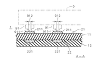
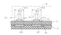
図1は、本発明の一の実施の形態に係る可撓性を有する配線基板(以下、「FPC」という。)1を示す断面図であり、図2はFPC1の平面図である。図1に示すように、FPC1は多層基板であり、樹脂(例えば、ポリイミド)で形成された2つの絶縁層11,12を備え、上側の絶縁層11の上下の主面には、それぞれ銅箔のパターンである配線層21,22が設けられる。なお、図2に示すように、配線層21,22は絶縁層11の両主面に沿って配線パターンとして広がっているが、図1では図2中の矢印A−Aでの断面における配線層21,22の極一部(符号211,221を付す部分)のみが図示されている。
FIG. 1 is a cross-sectional view showing a flexible wiring board (hereinafter referred to as “FPC”) 1 according to an embodiment of the present invention, and FIG. 2 is a plan view of the
配線層21は表面に露出しており、加圧を伴う接合により図1中に2点鎖線にて示す電子部品9の複数のバンプ91がそれぞれ接合される複数の電極211を備える。電子部品9はいわゆる半導体のベアチップであり、バンプ91は電子部品9のアルミ電極上に形成されている。なお、バンプとしては、ワイヤボンディング法を応用したいわゆるスタッドバンプ、メッキ工程により形成したメッキバンプ、はんだを用いたはんだバンプ等の様々なものが利用可能である。電子部品9の実装では、例えば、電子部品9を加熱しつつ、樹脂中に金属粒子を拡散させた異方性導電フィルムやペーストを挟んでバンプ91を電極211に押圧する接合、非導電フィルムやペーストを挟んでバンプ91を電極211に押圧する接合、電子部品9に超音波を付与しつつバンプ91を電極211に押圧する接合等、様々な接合方法が採用される。
The
配線層22は、配線層21側から2番目の配線層であり、配線層22のパターンは複数のバンプ91のそれぞれの接合中心911と重なる(すなわち、接合中心911と対向する)対向部221を備える。図2では配線層22が有する複数の直線状の配線のうち、電極211と対向する部位に符号221を付している。すなわち、対向部221は配線として利用される。また、対向部221は、バンプ91のそれぞれの接合領域(図1中に符号912を付す領域)の全体と重なる大きさとされる。
The
配線層22に対向部221を設けることにより、FPC1では電子部品9が実装される際に、各電極211が水平姿勢のまま同様に押し込まれる(すなわち、絶縁層11,12が同じ程度撓む)こととなる。その結果、電子部品9の各バンプ91が電極211に同様の力で押圧され(バンプ91の先端が尖っている場合には同様に押し潰され)、電子部品9がFPC1に高い信頼性にて接合される。
By providing the facing
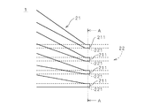
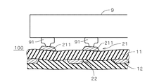
これに対し、配線層22において電極211に対向する部位が存在したり存在しなかったりした場合、あるいは、部分的に重なる場合(以下、「比較例」という。)には、電子部品9の実装時に全ての電極211が均一に押し込まれなかったり、傾いたりするため、接合不良が生じるおそれがある。図3は比較例における実装時のFPC100の断面および電子部品9を示す図であり、図4はFPC100の平面図である。図3に示すように、配線層22のパターンが存在する領域ではFPC100の撓み量が相対的に減少するため、バンプ91に押圧された場合に配線層21の電極211が傾いたり、場合によっては2つの電極211の押し込まれる距離(接合時の沈み量)(以下、電極211の傾きや沈み量を「押し込まれ量」と総称する。)が異なってしまうこととなる。
On the other hand, when the part facing the
ところで、電極211にバンプ91が押圧される際には、図1に示すように電極211とバンプ91との接合領域912の中心である接合中心911の真下において絶縁層11,12内に最も大きな応力が発生するため、配線層22のパターンが複数のバンプ91のそれぞれの接合中心911と重なることが電極211の押し込まれ量のばらつきを抑えるために最低限必要となる。また、接合領域912全体で電極211が押圧されることから、配線層22のパターンが、複数のバンプ91のそれぞれの接合領域912全体と重なることがより好ましいといえる。そして、電極211の押し込まれ量のばらつき防止のこれらの原理に基づいて図4に示すFPC100に対して設計変更を行うことにより、図2に示すFPC1が得られることとなる。
By the way, when the
さらに、対向部221が実際に使用される配線に含まれることにより、用途のない対向部を設けて他の配線を迂回させる場合よりも設計変更を容易に行うことができる。
Furthermore, by including the facing
図5は、より高い接合信頼性にて電子部品9を実装することができるFPC1aを示す断面図である。FPC1aでは配線層22の対向部221の幅が図1に示すものから拡大されているという点で異なっている。その他は同様であり、図1と同符号を付している。既に述べたように、配線層22のパターンは複数のバンプ91のそれぞれの接合領域912全体と重なることが好ましい。しかしながら、実際には、実装時の電子部品9の位置合わせ精度やFPCを製造する際の配線層21と配線層22との位置合わせ精度には限界がある。そこで、図5に示すFPC1aでは、配線層22のパターンに含まれる対向部221が、複数のバンプ91のそれぞれの接合領域912を、バンプ91の接合誤差および配線層21と配線層22との間の誤差の分だけ拡大した領域913全体と重なるように形成される。これにより、対向部221は接合領域912と確実に重なることとなり、接合の信頼性がさらに向上される。
FIG. 5 is a cross-sectional view showing the FPC 1a capable of mounting the electronic component 9 with higher bonding reliability. The FPC 1a is different in that the width of the facing
図6は、両面に電子部品の実装が行われるFPC1bを示す図である。FPC1bは、複数の絶縁層11〜13を備え、上面から下面に向かって各絶縁層の境界(上下の露出面を含む。)に配線層21〜24を備える。FPC1bのように配線層21が形成された露出面とは反対側の露出面上に形成された配線層24が存在する場合は、電子部品9の実装時のFPC1bの撓みは配線層24の影響を大きく受けるため、配線層24に、配線層21の電極211に対向する(すなわち、バンプと電極211との接合中心と重なる)対向部241が設けられる。これにより、電子部品9を実装する際の接合の信頼性が向上される。また、従来のように裏面にて電子部品の実装可能な領域が補強板により制限されることも防止される。
FIG. 6 is a diagram showing the
なお、絶縁層が比較的硬く、かつ、厚い場合は、実装時の電極211の押し込まれ量は、図1の場合と同様に配線層21側から2番目の配線層22の影響を大きく受けるため、配線層22に対向部が設けられることが好ましい。一般的には、バンプが接合される配線層から2番目の配線層またはバンプが接合される配線層とは反対側の露出面上に形成された配線層に対向部が設けられることが好ましいといえる。
If the insulating layer is relatively hard and thick, the amount of the
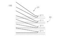
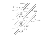
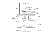
図7および図8は、図1の対向部221や図6の対向部241に対応する対向部281(または281a,281b)を有する配線層28のパターンを電子部品9と共に示す平面図である。なお、図7および図8では、他の配線層の図示を省略し、配線層28のみを実線にて示している。
7 and 8 are plan views showing the pattern of the
図7では、配線層28の1つの配線282が2つの接合領域912と重なる対向部281を有する。このように、電子部品9のバンプのピッチに対して配線のピッチが大きい場合には、配線を広げるなどして複数の接合領域912と重なる対向部281、すなわち、バンプの接合中心に重なる複数の部位を含む対向部281が設けられてもよい。図7に示すFPCにおいても、図1の場合と同様に複数の対向部281が複数の配線に含まれることにより、接合領域912の存在を考慮しつつ簡単な設計変更にて対向部281を設けることができる。
In FIG. 7, one
図8は、さらに複雑な配線層28を例示する図である。図8に示す配線層28は、図7の場合と同様に、接合領域912に重なる対向部281a,281bを有する配線282a,282bが設けられ、さらに、他の配線283が対向部281aの間へと入り込んだり、配線284が対向部281aの間を通り抜けたりする。対向部281aは、例えば、ビアと接続されて他の配線層に接続され、配線283の先端もビアと接続されてさらに他の配線層に接続される。このように、対向部281aを接合領域912に合わせて局所的に設けることにより、配線層28の機能を損なうことなく対向部を設けることが容易に実現される。
FIG. 8 is a diagram illustrating a more
以上、本発明の実施の形態について説明してきたが、本発明は上記実施の形態に限定されるものではなく、様々な変形が可能である。 Although the embodiments of the present invention have been described above, the present invention is not limited to the above-described embodiments, and various modifications can be made.
例えば、絶縁層や配線層の数は上記実施の形態に例示したものより多くてもよく、逆に、絶縁層が1つであり、絶縁層の両主面のそれぞれに配線層が形成されるのみであってもよい。すなわち、本発明が適用されるFPCは複数の配線層と、この複数の配線層の間に設けられた少なくとも1つの絶縁層とを備えるものとされる。 For example, the number of insulating layers and wiring layers may be larger than those exemplified in the above embodiment, and conversely, there is one insulating layer, and wiring layers are formed on both main surfaces of the insulating layer. It may be only. That is, the FPC to which the present invention is applied includes a plurality of wiring layers and at least one insulating layer provided between the plurality of wiring layers.
また、既述のように、加圧を伴う接合によりバンプがFPCの電極と接合されるが、接合が行われる配線層以外の配線層に対向部を設ける手法は、絶縁層が撓みやすい加圧および加熱を伴う接合に特に適している。例えば、接合時に接着剤である熱硬化性の樹脂の加熱が行われる場合に適している。 In addition, as described above, the bump is bonded to the FPC electrode by bonding involving pressurization, but the method of providing the facing portion in the wiring layer other than the wiring layer to be bonded is the pressurization in which the insulating layer is easily bent. And particularly suitable for bonding with heating. For example, it is suitable when a thermosetting resin that is an adhesive is heated during bonding.
また、上記実施の形態では、配線基板としてFPCを例示したが、硬い材料で形成されているが薄いために可撓性を有する配線基板に対しても、配線層に対向部を設ける技術を適用することができる。さらに、対向部に対向する電極に実装される電子部品は、半導体のベアチップには限定されず、バンプを有する他の種類の電子部品(例えば、パッケージ化された電子部品)の実装にも利用することができる。 In the above embodiment, the FPC is exemplified as the wiring board. However, the technique of providing the facing portion in the wiring layer is also applied to the wiring board having flexibility because it is made of a hard material but is thin. can do. Furthermore, the electronic component mounted on the electrode facing the facing portion is not limited to a semiconductor bare chip, and is also used for mounting other types of electronic components having bumps (for example, packaged electronic components). be able to.
本発明は、電子部品が実装される可撓性を有する多層の様々な配線基板に利用することができる。 The present invention can be used for various flexible multilayer wiring boards on which electronic components are mounted.
1,1a,1b FPC
9 電子部品
11〜13 絶縁層
21〜24,28 配線層
91 バンプ
211 電極
221,241,281a,281b 対向部
282,282a,282b 配線
911 接合中心
912 接合領域
1,1a, 1b FPC
DESCRIPTION OF SYMBOLS 9 Electronic component 11-13 Insulation layer 21-24, 28
Claims (6)
複数の配線層と、
前記複数の配線層の間に設けられた少なくとも1つの絶縁層と、
を備え、
前記複数の配線層のうちの表面に露出する一の配線層が、加圧を伴う接合により電子部品の複数のバンプがそれぞれ接合される複数の電極を備え、
前記複数の配線層のうちの他の一の配線層のパターンが、前記複数のバンプのそれぞれの接合中心と重なることを特徴とする配線基板。 A wiring board having flexibility,
Multiple wiring layers;
At least one insulating layer provided between the plurality of wiring layers;
With
One wiring layer exposed on the surface of the plurality of wiring layers includes a plurality of electrodes to which a plurality of bumps of an electronic component are respectively bonded by bonding with pressurization,
A wiring board, wherein a pattern of another wiring layer of the plurality of wiring layers overlaps with a bonding center of each of the plurality of bumps.
前記他の一の配線層のパターンのうち前記複数のバンプの接合中心に重なる部位が、配線に含まれることを特徴とする配線基板。 The wiring board according to claim 1,
The wiring board is characterized in that a portion of the pattern of the other wiring layer that overlaps the bonding center of the plurality of bumps is included in the wiring.
前記他の一の配線層のパターンのうち前記複数のバンプの接合中心に重なる部位が、複数の配線に含まれることを特徴とする配線基板。 The wiring board according to claim 2,
A part of the pattern of the other wiring layer that overlaps the bonding center of the plurality of bumps is included in the plurality of wirings.
前記他の一の配線層のパターンが、前記複数のバンプのそれぞれの接合領域全体と重なることを特徴とする配線基板。 The wiring board according to any one of claims 1 to 3,
The wiring board, wherein the pattern of the other wiring layer overlaps the entire bonding region of each of the plurality of bumps.
前記他の一の配線層のパターンが、前記複数のバンプのそれぞれの接合領域を、バンプの接合誤差および前記一の配線層と前記他の一の配線層との間の誤差の分だけ拡大した領域全体と重なることを特徴とする配線基板。 The wiring board according to claim 4,
The pattern of the one other wiring layer expands the bonding region of each of the plurality of bumps by a bonding error of the bump and an error between the one wiring layer and the one other wiring layer. A wiring board characterized by overlapping the entire region.
前記他の一の配線層が、前記一の配線層側から2番目の配線層または前記一の配線層が形成された露出面とは反対側の露出面上に形成された配線層であることを特徴とする配線基板。 The wiring board according to any one of claims 1 to 5,
The other wiring layer is a wiring layer formed on the second wiring layer from the one wiring layer side or an exposed surface opposite to the exposed surface on which the one wiring layer is formed. A wiring board characterized by.
Priority Applications (1)
| Application Number | Priority Date | Filing Date | Title |
|---|---|---|---|
| JP2004108828A JP2005294615A (en) | 2004-04-01 | 2004-04-01 | Wiring board |
Applications Claiming Priority (1)
| Application Number | Priority Date | Filing Date | Title |
|---|---|---|---|
| JP2004108828A JP2005294615A (en) | 2004-04-01 | 2004-04-01 | Wiring board |
Publications (1)
| Publication Number | Publication Date |
|---|---|
| JP2005294615A true JP2005294615A (en) | 2005-10-20 |
Family
ID=35327196
Family Applications (1)
| Application Number | Title | Priority Date | Filing Date |
|---|---|---|---|
| JP2004108828A Pending JP2005294615A (en) | 2004-04-01 | 2004-04-01 | Wiring board |
Country Status (1)
| Country | Link |
|---|---|
| JP (1) | JP2005294615A (en) |
Cited By (4)
| Publication number | Priority date | Publication date | Assignee | Title |
|---|---|---|---|---|
| JP2008164427A (en) * | 2006-12-28 | 2008-07-17 | Micronics Japan Co Ltd | Probe unit board |
| WO2009022522A1 (en) * | 2007-08-10 | 2009-02-19 | Sharp Kabushiki Kaisha | Wiring board and liquid crystal display device |
| US8310645B2 (en) | 2008-06-25 | 2012-11-13 | Sharp Kabushiki Kaisha | Wiring board and liquid crystal display device |
| JP2013065810A (en) * | 2011-08-31 | 2013-04-11 | Denso Corp | Multilayer substrate |
-
2004
- 2004-04-01 JP JP2004108828A patent/JP2005294615A/en active Pending
Cited By (5)
| Publication number | Priority date | Publication date | Assignee | Title |
|---|---|---|---|---|
| JP2008164427A (en) * | 2006-12-28 | 2008-07-17 | Micronics Japan Co Ltd | Probe unit board |
| WO2009022522A1 (en) * | 2007-08-10 | 2009-02-19 | Sharp Kabushiki Kaisha | Wiring board and liquid crystal display device |
| US8319932B2 (en) | 2007-08-10 | 2012-11-27 | Sharp Kabushiki Kaisha | Wiring board and liquid crystal display device |
| US8310645B2 (en) | 2008-06-25 | 2012-11-13 | Sharp Kabushiki Kaisha | Wiring board and liquid crystal display device |
| JP2013065810A (en) * | 2011-08-31 | 2013-04-11 | Denso Corp | Multilayer substrate |
Similar Documents
| Publication | Publication Date | Title |
|---|---|---|
| JP2664873B2 (en) | Electronic package and manufacturing method thereof | |
| JP2004343030A (en) | Printed circuit board, method of manufacturing the same, and circuit module provided with the printed circuit board | |
| EP1005086A2 (en) | Metal foil having bumps, circuit substrate having the metal foil, and semiconductor device having the circuit substrate | |
| JP2004179232A (en) | Semiconductor device, method of manufacturing the same, and electronic device | |
| CN1312764C (en) | Electronic component device and producing method thereof | |
| JP4813255B2 (en) | WIRING BOARD, MANUFACTURING METHOD THEREOF, AND SEMICONDUCTOR DEVICE | |
| JP2001223243A (en) | Semiconductor device and its manufacturing method, circuit board, and electronic equipment | |
| JP2005294615A (en) | Wiring board | |
| JP2002290028A (en) | Connection method and connection structure of printed wiring board | |
| JP3438583B2 (en) | Anisotropic conductive film connection method | |
| JP2002261416A (en) | Electrode connection structure | |
| JP2000022329A (en) | Wiring board, electronic unit and electronic component mounting method | |
| JP5277754B2 (en) | Flip connection mounting body and method of manufacturing flip connection mounting body | |
| CN208128619U (en) | Resin substrates and components mounted resin substrates | |
| KR100516815B1 (en) | Semiconductor device | |
| JP2821070B2 (en) | Composite printed circuit board joining method | |
| JP7351552B2 (en) | Board, board manufacturing method, and board connection method | |
| JP3627895B2 (en) | Wiring board | |
| JP4520052B2 (en) | Semiconductor device and manufacturing method thereof | |
| JP4619104B2 (en) | Semiconductor device | |
| JP4430419B2 (en) | Electronic circuit using parallel conductive circuit sheet and method for manufacturing the same | |
| CN100499054C (en) | Semiconductor device and method for manufacturing the same | |
| JP4342577B2 (en) | Semiconductor chip mounting structure | |
| JP2002057416A (en) | Flexible wiring board for both-side connection | |
| JP2009278050A (en) | Electronic module, wiring board, method for manufacturing electronic module, and method for manufacturing wiring board |
Legal Events
| Date | Code | Title | Description |
|---|---|---|---|
| A621 | Written request for application examination |
Free format text: JAPANESE INTERMEDIATE CODE: A621 Effective date: 20061128 |
|
| RD01 | Notification of change of attorney |
Free format text: JAPANESE INTERMEDIATE CODE: A7421 Effective date: 20061213 |
|
| A977 | Report on retrieval |
Free format text: JAPANESE INTERMEDIATE CODE: A971007 Effective date: 20090120 |
|
| A131 | Notification of reasons for refusal |
Free format text: JAPANESE INTERMEDIATE CODE: A131 Effective date: 20090217 |
|
| A521 | Request for written amendment filed |
Free format text: JAPANESE INTERMEDIATE CODE: A523 Effective date: 20090416 |
|
| A02 | Decision of refusal |
Free format text: JAPANESE INTERMEDIATE CODE: A02 Effective date: 20090825 |