JP2005294443A - Semiconductor device and manufacturing method thereof - Google Patents
Semiconductor device and manufacturing method thereof Download PDFInfo
- Publication number
- JP2005294443A JP2005294443A JP2004105834A JP2004105834A JP2005294443A JP 2005294443 A JP2005294443 A JP 2005294443A JP 2004105834 A JP2004105834 A JP 2004105834A JP 2004105834 A JP2004105834 A JP 2004105834A JP 2005294443 A JP2005294443 A JP 2005294443A
- Authority
- JP
- Japan
- Prior art keywords
- back surface
- semiconductor device
- semiconductor element
- terminal
- semiconductor
- Prior art date
- Legal status (The legal status is an assumption and is not a legal conclusion. Google has not performed a legal analysis and makes no representation as to the accuracy of the status listed.)
- Pending
Links
Images

Classifications
-
- H—ELECTRICITY
- H10—SEMICONDUCTOR DEVICES; ELECTRIC SOLID-STATE DEVICES NOT OTHERWISE PROVIDED FOR
- H10W—GENERIC PACKAGES, INTERCONNECTIONS, CONNECTORS OR OTHER CONSTRUCTIONAL DETAILS OF DEVICES COVERED BY CLASS H10
- H10W72/00—Interconnections or connectors in packages
- H10W72/01—Manufacture or treatment
- H10W72/0198—Manufacture or treatment batch processes
-
- H—ELECTRICITY
- H10—SEMICONDUCTOR DEVICES; ELECTRIC SOLID-STATE DEVICES NOT OTHERWISE PROVIDED FOR
- H10W—GENERIC PACKAGES, INTERCONNECTIONS, CONNECTORS OR OTHER CONSTRUCTIONAL DETAILS OF DEVICES COVERED BY CLASS H10
- H10W72/00—Interconnections or connectors in packages
- H10W72/50—Bond wires
- H10W72/541—Dispositions of bond wires
- H10W72/5449—Dispositions of bond wires not being orthogonal to a side surface of the chip, e.g. fan-out arrangements
-
- H—ELECTRICITY
- H10—SEMICONDUCTOR DEVICES; ELECTRIC SOLID-STATE DEVICES NOT OTHERWISE PROVIDED FOR
- H10W—GENERIC PACKAGES, INTERCONNECTIONS, CONNECTORS OR OTHER CONSTRUCTIONAL DETAILS OF DEVICES COVERED BY CLASS H10
- H10W72/00—Interconnections or connectors in packages
- H10W72/90—Bond pads, in general
- H10W72/931—Shapes of bond pads
- H10W72/932—Plan-view shape, i.e. in top view
-
- H—ELECTRICITY
- H10—SEMICONDUCTOR DEVICES; ELECTRIC SOLID-STATE DEVICES NOT OTHERWISE PROVIDED FOR
- H10W—GENERIC PACKAGES, INTERCONNECTIONS, CONNECTORS OR OTHER CONSTRUCTIONAL DETAILS OF DEVICES COVERED BY CLASS H10
- H10W74/00—Encapsulations, e.g. protective coatings
-
- H—ELECTRICITY
- H10—SEMICONDUCTOR DEVICES; ELECTRIC SOLID-STATE DEVICES NOT OTHERWISE PROVIDED FOR
- H10W—GENERIC PACKAGES, INTERCONNECTIONS, CONNECTORS OR OTHER CONSTRUCTIONAL DETAILS OF DEVICES COVERED BY CLASS H10
- H10W74/00—Encapsulations, e.g. protective coatings
- H10W74/10—Encapsulations, e.g. protective coatings characterised by their shape or disposition
- H10W74/131—Encapsulations, e.g. protective coatings characterised by their shape or disposition the semiconductor body being only partially enclosed
- H10W74/142—Encapsulations, e.g. protective coatings characterised by their shape or disposition the semiconductor body being only partially enclosed the encapsulations exposing the passive side of the semiconductor body
-
- H—ELECTRICITY
- H10—SEMICONDUCTOR DEVICES; ELECTRIC SOLID-STATE DEVICES NOT OTHERWISE PROVIDED FOR
- H10W—GENERIC PACKAGES, INTERCONNECTIONS, CONNECTORS OR OTHER CONSTRUCTIONAL DETAILS OF DEVICES COVERED BY CLASS H10
- H10W90/00—Package configurations
- H10W90/701—Package configurations characterised by the relative positions of pads or connectors relative to package parts
- H10W90/751—Package configurations characterised by the relative positions of pads or connectors relative to package parts of bond wires
- H10W90/756—Package configurations characterised by the relative positions of pads or connectors relative to package parts of bond wires between a chip and a stacked lead frame, conducting package substrate or heat sink
Landscapes
- Encapsulation Of And Coatings For Semiconductor Or Solid State Devices (AREA)
- Lead Frames For Integrated Circuits (AREA)
Abstract
【課題】 安価なリードフレームを用い、ダイパッドを不要にして、半導体装置の薄型化、小型化、多ピン化を低コストで実現し、半導体素子を安定に固定し、接続信頼性及び封止の安定性、更には実装の信頼性と安定性を向上させること。
【解決手段】 リードフレーム24から作製された端子(外部端子)5と半導体素子(ICチップ)1とがワイヤ4でワイヤボンディングされ、封止樹脂7で封止され、半導体素子1の裏面に接して絶縁性樹脂層21が予めコーティング等で形成され、この絶縁性樹脂層21が封止樹脂7の裏面側に露出しており、端子5の裏面と同一平面上に存在している装置(半導体パッケージ)20。
【選択図】 図1
PROBLEM TO BE SOLVED: To achieve a reduction in thickness, size, and number of pins of a semiconductor device at a low cost by using an inexpensive lead frame, eliminating a die pad, stably fixing a semiconductor element, and connecting reliability and sealing. To improve stability, and further, mounting reliability and stability.
A terminal (external terminal) 5 and a semiconductor element (IC chip) 1 manufactured from a lead frame 24 are wire-bonded with a wire 4, sealed with a sealing resin 7, and contacted with a back surface of the semiconductor element 1. The insulating resin layer 21 is previously formed by coating or the like, and this insulating resin layer 21 is exposed on the back side of the sealing resin 7 and is present on the same plane as the back side of the terminal 5 (semiconductor Package) 20.
[Selection] Figure 1
Description
本発明は、半導体素子と端子とが接続され、封止材で封止された半導体装置及びその製造方法に関するものである。 The present invention relates to a semiconductor device in which a semiconductor element and a terminal are connected and sealed with a sealing material, and a manufacturing method thereof.
近年の電子機器への要求は、小型、薄型、軽量、高性能、高機能、低コストなどであるが、SIP(System In Package)等は、まさにこれらの要求から生み出されたものである。しかしながら、半導体集積回路(IC)チップを実装するためのインターポーザーと呼ばれる配線回路基板が必要であるため、低コスト化、薄型化の要求を十分に満足していない。 In recent years, demands for electronic devices are small, thin, lightweight, high performance, high functionality, low cost, etc. SIP (System In Package) and the like have been created from these demands. However, since a printed circuit board called an interposer for mounting a semiconductor integrated circuit (IC) chip is required, the demands for cost reduction and thickness reduction are not fully satisfied.
図8には、ダイパッド非露出型の半導体装置(半導体パッケージ)10を示すが、これは、安価なリードフレームを用い、隅部のリード部6で支持されたダイパッド3上に半導体素子であるICチップ1をダイボンド材8によって固定し、金属ワイヤ4によってICチップ1の電極パッド2と端子5とをワイヤボンディングで接続し、端子5の裏面及び側面以外をモールド樹脂7で封止したものである(例えば後記の特許文献1参照)。
FIG. 8 shows a die pad non-exposed semiconductor device (semiconductor package) 10, which uses an inexpensive lead frame and is an IC that is a semiconductor element on a die pad 3 supported by a
この半導体パッケージでは、リードフレームから作製された端子5が外部(接続)端子として用いられ、プリント配線板(図示せず)に直接はんだ付けされて実装される。
In this semiconductor package,
一方、リードフレームから作製された端子を用いるが、上記のようなダイパッドは用いないで樹脂封止したパッケージ(例えば後記の特許文献2参照)や、リードフレーム及びダイパッドを共に用いないで樹脂封止したパッケージ(例えば後記の特許文献3参照)も知られている。
On the other hand, although a terminal manufactured from a lead frame is used, a resin-sealed package (for example, refer to
図8に示した如き特許文献1に示されたダイパッド非露出型の半導体装置10は、ダイパッド3を半導体装置内部にディプレス加工でアップセットしてダイパッド3の非露出化を実現しているため、次の(1)〜(5)の問題点がある。
The die pad
(1)ダイパッド3を露出させたパッケージと比較して、半導体装置の薄型化が困難で ある。 (1) It is difficult to reduce the thickness of the semiconductor device as compared with the package in which the die pad 3 is exposed.
(2)ダイパッド3及びそれを支える吊り部6が必要であり、半導体装置の小型化及び 多ピン化の妨げとなる。
(2) The die pad 3 and the
(3)ダイパッド3の下面をハーフエッチングしたもの(図示せず)が知られているが 、この場合も、リードフレームに樹脂フィルムを貼り付けてダイボンドするときに、ダ イパッド3の沈み込みが発生するので、半導体素子1を所定の位置に搭載し難くなる。
(3) Although the bottom surface of the die pad 3 is half-etched (not shown) is known, in this case also, the die pad 3 sinks when a resin film is attached to the lead frame and die bonded. Therefore, it becomes difficult to mount the
(4)また、そのようにリードフレームに樹脂フィルムを貼り付ける場合、樹脂フィル ムが破れる等の問題があり、ヒートプレートをダイパッド部に接触させるのが困難であ るため、ワイヤボンディング時の熱、荷重、超音波が半導体素子1に均一に伝わらず、 ワイヤボンディングの接続不良が発生し易い。
(4) Also, when a resin film is attached to the lead frame in this way, there is a problem such as the resin film being torn, and it is difficult to bring the heat plate into contact with the die pad part. , Load and ultrasonic waves are not uniformly transmitted to the
(5)また、射出成形等で樹脂封止7を行なう場合に、ダイパッド3のシフト等が発生 し、ボンディングワイヤ4の切断等の不良が発生し易いと共に、ダイパッド3裏面への 樹脂の充填性が悪く、ボイドや未充填等の不良が発生し易い。
(5) Further, when the resin sealing 7 is performed by injection molding or the like, the die pad 3 is shifted, and defects such as cutting of the
また、特許文献2に示された半導体パッケージでは、ダイパッド自体をなくして半導体素子の裏面が露出しているので、上記した問題はある程度は解消されるものの、実装過程において半導体素子の裏面の損傷が生じ易いと共に、プリント配線板への実装時に絶縁手段をプリント配線板側に設ける必要があって、実装の作業性及び信頼性に問題がある。
Further, in the semiconductor package disclosed in
また、特許文献3に示された半導体パッケージでは、半導体素子の裏面は絶縁材で保護されるが、端子がリードフレームから作製されるものではなく、メタルフレーム上への金属ワイヤの接続後にメタルフレームを溶解除去してワイヤ付きの端子を形成しているので、端子の形成がそれ程容易ではなく、その接合強度も不十分となり、更にはプリント配線板への接合も不良となり易いので、端子部にはスタッド端子を付加する必要がある。 In the semiconductor package disclosed in Patent Document 3, the back surface of the semiconductor element is protected by an insulating material, but the terminal is not manufactured from the lead frame, and the metal frame is connected after the metal wire is connected to the metal frame. Since the terminal with wire is formed by dissolving and removing the terminal, the terminal is not so easy to form, its bonding strength is insufficient, and further, the bonding to the printed wiring board tends to be poor. It is necessary to add a stud terminal.
本発明の目的は、安価なリードフレームを用い、ダイパッドを不要にして、半導体装置の薄型化、小型化、多ピン化を低コストで実現し、半導体素子を安定に固定し、接続信頼性及び封止の安定性、更には実装の信頼性と安定性を向上させることにある。 An object of the present invention is to use an inexpensive lead frame, eliminate the need for a die pad, realize a reduction in thickness, size, and number of pins of a semiconductor device at low cost, stably fix a semiconductor element, and improve connection reliability and It is to improve the stability of sealing, and further the reliability and stability of mounting.
即ち、本発明は、リードフレームから作製された端子と半導体素子とが接続され、封止材で封止された半導体装置において、前記半導体素子の裏面に接して絶縁物質層が形成され、この絶縁物質層が前記封止材の裏面側に露出していることを特徴とする半導体装置に係るものである。 That is, according to the present invention, in a semiconductor device in which a terminal manufactured from a lead frame and a semiconductor element are connected and sealed with a sealing material, an insulating material layer is formed in contact with the back surface of the semiconductor element. A substance layer is exposed on the back side of the sealing material.
本発明はまた、リードフレームから作製された端子と半導体素子とが接続され、封止材で封止された半導体装置の製造方法において、半導体ウェハの裏面に接して絶縁物質層を形成する工程と、前記半導体ウェハを個片化して、裏面に接して前記絶縁物質層が形成された半導体素子を得る工程と、この半導体素子をリードフレーム間に配置する工程と、前記絶縁物質層及び前記リードフレームの裏面を除いて前記半導体素子及び前記リードフレームを封止材で封止する工程と、前記リードフレームの所定箇所を前記封止材と共に切断して、前記端子を形成すると共に、前記絶縁物質層が前記封止材の裏面側に露出した半導体装置を得る工程とを有することを特徴とする半導体装置の製造方法も提供するものである。 The present invention also includes a step of forming an insulating material layer in contact with the back surface of a semiconductor wafer in a method of manufacturing a semiconductor device in which a terminal manufactured from a lead frame and a semiconductor element are connected and sealed with a sealing material. Separating the semiconductor wafer into individual pieces to obtain a semiconductor element in which the insulating material layer is formed in contact with the back surface; arranging the semiconductor element between lead frames; and the insulating material layer and the lead frame. A step of sealing the semiconductor element and the lead frame with a sealing material except for a back surface thereof, cutting predetermined portions of the lead frame together with the sealing material to form the terminals, and the insulating material layer And a step of obtaining a semiconductor device exposed on the back side of the encapsulant. A method of manufacturing a semiconductor device is also provided.
本発明の半導体装置及びその製造方法によれば、安価なリードフレームを用いて、半導体素子を接続する端子を形成し、前記半導体素子の裏面に接して形成された絶縁物質層を封止材の裏面側に露出させた構造とし、またこの構造を製造する方法として、半導体ウェハの裏面に接して絶縁物質層を形成した後に前記半導体ウェハを個片化して、裏面に接して前記絶縁物質層が形成された半導体素子を得、この半導体素子をリードフレーム間に配置して、前記絶縁物質層及び前記リードフレームの裏面を除いて前記半導体素子及び前記リードフレームを封止材で封止した後、前記リードフレームの所定箇所を前記封止材と共に切断して、前記端子を形成すると共に、前記絶縁物質層が前記封止材の裏面側に露出した半導体装置を得ているので、次の(a)〜(h)に示す顕著な作用効果を得ることができる。 According to the semiconductor device and the manufacturing method thereof of the present invention, a terminal for connecting a semiconductor element is formed using an inexpensive lead frame, and an insulating material layer formed in contact with the back surface of the semiconductor element is formed of a sealing material. The structure exposed on the back surface side, and as a method of manufacturing this structure, after forming the insulating material layer in contact with the back surface of the semiconductor wafer, the semiconductor wafer is separated into pieces, and the insulating material layer is in contact with the back surface. After obtaining the formed semiconductor element, disposing the semiconductor element between the lead frames, sealing the semiconductor element and the lead frame with a sealing material except for the insulating material layer and the back surface of the lead frame, Since a predetermined portion of the lead frame is cut together with the sealing material to form the terminal, the semiconductor device is obtained in which the insulating material layer is exposed on the back side of the sealing material. Can be obtained a remarkable action and effect shown in the (a) ~ (h).
(a)半導体素子を搭載するためのダイパッドが不要になり(ダイパッドに必要とされ る厚みが不要となり)、ダイパッドをアップセットする必要がないため、半導体装置の 薄型化が可能となる。 (A) A die pad for mounting a semiconductor element is not required (the thickness required for the die pad is not required), and there is no need to upset the die pad, so that the semiconductor device can be thinned.
(b)また、ダイパッドを非露出とするのに必要なダイパッドのディプレス加工も不要 になるので、リードフレームのコストダウンが図れる。 (B) In addition, since the die pad pressing process necessary for unexposing the die pad is not required, the cost of the lead frame can be reduced.
(c)ダイパッドのみならず、ダイパッド吊り部が不要となるため、外部端子を配置す る上での制約が緩和され、半導体装置の小型化及び多ピン化を実現できる。 (C) Since not only the die pad but also the die pad hanging portion is not necessary, restrictions on the arrangement of the external terminals are alleviated, and the semiconductor device can be miniaturized and the number of pins can be increased.
(d)ダイパッドを不要として半導体素子を絶縁物質層を介して樹脂フィルムに固定し て半導体素子をダイボンドできるので、ダイボンド時に半導体素子のずれが発生しにく い。 (D) Since the semiconductor element can be die-bonded by fixing the semiconductor element to the resin film through the insulating material layer without using a die pad, the semiconductor element is unlikely to be displaced during die-bonding.
(e)ダイパッドを不要として半導体素子は絶縁物質層を介して樹脂フィルムに直接固 定してワイヤボンディングできるので、ワイヤボンド時に熱、荷重、超音波が均一に伝 わり、ワイヤボンディングの接続信頼性が向上する。 (E) Since a semiconductor element can be directly fixed to a resin film via an insulating material layer and wire bonding can be performed without the need for a die pad, heat, load, and ultrasonic waves are uniformly transmitted during wire bonding, and the connection reliability of wire bonding Will improve.
(f)ダイパッドが不要であって、半導体素子の裏面を予め絶縁物質層で覆っておくた め、射出成形等での樹脂封止を行なう場合のダイパッドのシフトによるワイヤの切断等 や、ダイパッド裏面のボイド、未充填等の不良が発生しない。 (F) Since the die pad is unnecessary and the back surface of the semiconductor element is covered with an insulating material layer in advance, cutting of the wire by shifting the die pad when performing resin sealing by injection molding or the like, Defects such as voids and unfilled will not occur.
(g)半導体素子の裏面が予め絶縁物質層で保護されているので、実装過程において半 導体素子の裏面の損傷を防止でき、かつプリント配線板への実装時にプリント配線板と 半導体素子との絶縁を容易に行い、実装信頼性が向上する。 (G) Since the back surface of the semiconductor element is protected in advance by an insulating material layer, it is possible to prevent damage to the back surface of the semiconductor element during the mounting process, and to insulate the printed wiring board from the semiconductor element when mounted on the printed wiring board. To improve mounting reliability.
(h)リードフレームから端子を形成し、これに半導体素子をワイヤボンディングする ことによって、端子の形成が容易であると同時に、端子での接合強度が十分となり、接 合不良をなくすことができる。 (H) By forming a terminal from the lead frame and wire bonding the semiconductor element to the terminal frame, it is easy to form the terminal, and at the same time, the bonding strength at the terminal is sufficient, and the bonding failure can be eliminated.
本発明の半導体装置及びその製造方法においては、前記半導体素子が前記端子にワイヤボンディングで接続され、リードフレームから加工された前記端子が外部(接続)端子として前記封止材の少なくとも裏面側に露出していることが望ましい。 In the semiconductor device and the manufacturing method thereof according to the present invention, the semiconductor element is connected to the terminal by wire bonding, and the terminal processed from the lead frame is exposed as an external (connection) terminal at least on the back surface side of the sealing material. It is desirable that
このためには、前記リードフレームを支持体上に固定した後、前記半導体ウェハの個片化によって得られた前記半導体素子を前記絶縁物質層の側で前記リードフレームのない前記支持体上に固定し、前記半導体素子と前記リードフレームとをワイヤボンディングで接続し、前記封止材を前記半導体素子及び前記リードフレーム上に被着し、更に前記リードフレームの所定箇所を前記封止材と共に切断して、前記封止材の少なくとも裏面側に前記端子を外部端子として露出させると共に前記封止材の裏面側に前記絶縁物質層を露出させた前記半導体装置を得るのがよい。 For this purpose, after fixing the lead frame on the support, the semiconductor element obtained by dividing the semiconductor wafer is fixed on the support without the lead frame on the insulating material layer side. The semiconductor element and the lead frame are connected by wire bonding, the sealing material is deposited on the semiconductor element and the lead frame, and a predetermined portion of the lead frame is cut together with the sealing material. It is preferable to obtain the semiconductor device in which the terminal is exposed as an external terminal at least on the back surface side of the sealing material and the insulating material layer is exposed on the back surface side of the sealing material.
この場合、半導体素子をリードフレームにワイヤボンディングすることによって、ボンディング接続部の接合強度が良好であって熱的ストレスに十分に耐え、また低コストでの接続を行うことができる。そして、前記絶縁物質層の裏面と前記封止材及び前記端子の裏面とを同一面上に存在させるのが、パッケージの薄型化に有利であると共に、樹脂フィルム等に半導体素子及び端子を安定して保持し、ワイヤボンディング及び樹脂封止を安定かつ信頼性良く高歩留で行うことができる。 In this case, by wire bonding the semiconductor element to the lead frame, the bonding strength of the bonding connection portion is good, it can sufficiently withstand thermal stress, and can be connected at low cost. In addition, it is advantageous for making the package thinner, and it is possible to stabilize the semiconductor element and the terminal on the resin film or the like by allowing the back surface of the insulating material layer and the back surface of the sealing material and the terminal to exist on the same surface. And wire bonding and resin sealing can be performed stably and reliably with high yield.
この絶縁物質層は、絶縁性樹脂層、絶縁膜、絶縁基板又は片面接着テープからなり、前記半導体ウェハの裏面に形成しておくのがよい。 The insulating material layer is made of an insulating resin layer, an insulating film, an insulating substrate, or a single-sided adhesive tape, and is preferably formed on the back surface of the semiconductor wafer.
この場合、前記半導体ウェハの裏面に、前記絶縁性樹脂層をスピンコート、トランスファー形成、印刷又はポッティングにより形成し、絶縁膜をスパッタ又は蒸着により形成し、前記絶縁基板を接着し、前記片面接着テープを接着することができる。 In this case, the insulating resin layer is formed on the back surface of the semiconductor wafer by spin coating, transfer formation, printing or potting, the insulating film is formed by sputtering or vapor deposition, the insulating substrate is bonded, and the single-sided adhesive tape Can be glued.
次に、本発明の好ましい実施の形態を図面参照下に説明する。 Next, a preferred embodiment of the present invention will be described with reference to the drawings.
第1の実施の形態
図1〜図4は、本発明の第1の実施の形態を示すものである。
First Embodiment FIGS. 1 to 4 show a first embodiment of the present invention.
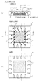
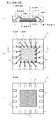
図1(A)は本実施の形態による半導体装置(半導体パッケージ)20の断面図、図1(B)はその平面図、図1(C)はその裏面図である。この半導体装置20は、半導体素子(ICチップ)1の裏面に予めコーティングした絶縁性樹脂層21を半導体装置(又は封止材7)裏面に露出させ、かつリードフレームから作製された端子(外部端子)5の裏面及び側面も露出させ、絶縁性樹脂層21の裏面と端子5の裏面とを同一平面上に存在させた構造となっていることを特徴としている。その他は、図8に示した従来構造と同様である。
1A is a sectional view of a semiconductor device (semiconductor package) 20 according to the present embodiment, FIG. 1B is a plan view thereof, and FIG. 1C is a rear view thereof. This semiconductor device 20 has an
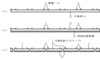
この半導体装置20を製造するには、まず、図3(a)に示すように、各素子領域を
作り込み、表面に各電極パッド2を形成した半導体ウェハ27の裏面に接して、図3(b)に示すように、エポキシ樹脂等の絶縁性樹脂層21をコーティングし、更に図3(c)に示すように、半導体ウェハ27をダイシングにより個片化して、裏面に接して絶縁性樹脂層21が形成された半導体素子1を作製する。
In order to manufacture the semiconductor device 20, first, as shown in FIG. 3A, each element region is formed and in contact with the back surface of the semiconductor wafer 27 on which the
ここで、半導体素子1裏面に絶縁性樹脂層21をウェハ状態でスピンコート、トランスファー成形、印刷、ポッティング等により形成した後、ダイシング装置によって個片に分割する。
Here, the insulating
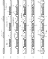
次いで、図2(a)に示すように、リードフレーム24と、リードフレーム24及び半導体素子1を固定するための樹脂フィルム25とを準備し、リードフレーム24を樹脂フィルム25上に固定する。このリードフレーム24は半導体装置が複数個取れる構造になっており、最終的に個片に分割される。この場合、予めNi−Pd−Au等のめっき処理がされたリードフレームを用いることもできる。
Next, as shown in FIG. 2A, a
次いで、図2(b)に示すように、裏面に予め絶縁性樹脂層21がコーティングされた半導体素子1をリードフレーム24間の樹脂フィルム25上の所定のエリアに接着する。
Next, as shown in FIG. 2B, the
次いで、図2(c)に示すように、半導体素子1の電極2とリードフレーム24のリード部(端子)5とをワイヤボンディング装置によってAu、Al等のワイヤ4で接続する。
Next, as shown in FIG. 2C, the
次いで、図2(d)に示すように、半導体装置全体を射出成形法やポッティング法、印刷法等によってエポキシ樹脂等の樹脂7で封止する。この封止樹脂7は、熱硬化性樹脂や紫外線硬化性樹脂等、半導体パッケージに用いられる一般的なものでよい。
Next, as shown in FIG. 2D, the entire semiconductor device is sealed with a
次いで、図2(e)に示すように、樹脂フィルム25に加熱処理、UV(紫外線)照射等を施して、樹脂フィルム25をピールオフにより除去する。リードフレーム24に予めめっき処理がされていない場合には、樹脂フィルム25の除去後にSn−BiやSn−Ag−Cu、Ni−Au等のめっき処理を行なう。
Next, as shown in FIG. 2E, the
次いで、図2(f)に示すように、リードフレーム24の所定箇所を封止樹脂7と共にダイシング装置によるブレード26で分割し、図1(A)に示した如き各半導体装置1に個片化する。
Next, as shown in FIG. 2 (f), a predetermined portion of the
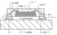
図4には、こうして得られた半導体装置1の端子5をはんだ23によってプリント配線板28上の接続ランド29に接合して、半導体装置1を実装した状態を示す。
FIG. 4 shows a state where the
本実施の形態によるパッケージ構造とその製造方法によれば、半導体素子1を搭載するためのダイパッドを不要としているので、ダイパッドに必要とされる厚みや、ダイパッド裏面を非露出とするためのディプレス加工によるダイパッドのアップセットが不要となるため、半導体装置20の薄型化とコストダウンが可能となる。
According to the package structure and the manufacturing method thereof according to the present embodiment, since the die pad for mounting the
また、ダイパッドのみならず、ダイパッド吊り部が不要となるため、外部端子5を配置する上での制約が緩和され、半導体装置20の小型化及び多ピン化を実現できる。
Further, since not only the die pad but also the die pad hanging portion is not necessary, restrictions on arranging the
そして、ダイパッドを不要として半導体素子1を絶縁性樹脂層21を介して樹脂フィルム25に固定して半導体素子1をダイボンドできるので、ダイボンド時に半導体素子1のずれが発生しにくくなると共に、その樹脂フィルム25に半導体素子1を絶縁性樹脂層21を介して固定してワイヤボンディングできるので、ワイヤボンド時に熱、荷重、超音波が均一に伝わり、ワイヤボンディングの接続信頼性が向上する。
Since the
また、ダイパッドが不要であって、ウェハ状態で個片化前の半導体素子1の裏面を予めエポキシ樹脂等の絶縁性樹脂層21で覆っておき、個片化後の半導体素子1を絶縁性樹脂層21を介して樹脂フィルム25上に固定しているので、射出成形等での樹脂封止を行なう場合のダイパッドのシフトによるワイヤ4の切断等や、ダイパッド裏面のボイド、未充填等の不良が発生しない。
In addition, a die pad is unnecessary, and the back surface of the
そして、半導体素子1の裏面が予め絶縁性樹脂層21で覆われて保護されているので、実装過程において半導体素子1の裏面の損傷を防止でき、かつ半導体素子1の裏面の電気的絶縁性を確保してプリント配線板28への実装時にプリント配線板28と半導体素子1との絶縁を容易に行い、実装信頼性が向上する。
Since the back surface of the
しかも、リードフレーム24から端子5を形成し、これに半導体素子1をワイヤボンディングすることによって、端子5の形成が容易であると同時に、端子5での接合強度が十分となり、接合不良をなくすことができる。
In addition, by forming the terminal 5 from the
なお、絶縁性樹脂層21は、上記の電気的絶縁性の確保のためには、20〜100μmの厚みを有することが望ましく、また材質的には、半導体素子1との間及び封止樹脂7との間にクラックが入り難いものであることが望ましく、封止樹脂7と熱膨張係数等の近いエポキシ系樹脂やポリイミド系樹脂からなるのがよい。
The insulating
また、半導体素子1をリードフレーム24にワイヤボンディングすることによって、ボンディング接続部の接合強度が良好であって熱的ストレスに十分に耐え、また低コストでの接続を行うことができる。そして、半導体素子の裏面に予め形成した絶縁性樹脂層21の裏面とリードフレーム24の裏面とを同一平面上に存在させているので、パッケージの薄型化に有利であると共に、樹脂フィルム25に半導体素子1及びリードフレーム24を安定して保持し、ワイヤボンディング及び樹脂封止を安定かつ信頼性良く高歩留で行うことができる。
Further, by wire-bonding the
第2の実施の形態
図5は、本発明の第2の実施の形態を示すものである。
Second Embodiment FIG. 5 shows a second embodiment of the present invention.
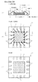
図5(A)は本実施の形態による半導体装置(半導体パッケージ)30の断面図、図5(B)はその平面図、図5(C)はその裏面図である。この半導体装置30は、半導体素子(ICチップ)1の裏面に予めスパッタリング又は真空蒸着で形成したSiO2等の絶縁膜31を半導体装置(または封止材7)裏面に露出させ、かつリードフレームから作製された端子(外部端子)5の裏面及び側面を露出させ、絶縁膜31の裏面と端子5の裏面とを同一平面上に存在させた構造となっていることを特徴としている。その他は、図8に示した従来構造と同様である。
5A is a sectional view of the semiconductor device (semiconductor package) 30 according to the present embodiment, FIG. 5B is a plan view thereof, and FIG. 5C is a rear view thereof. In this
本実施の形態によれば、半導体ウェハの状態でその裏面にSiO2等の絶縁膜31をスパッタリング等により成膜した後は、図2(a)〜(f)に示した工程によって図5に示した半導体パッケージ30を作製する。従って、上述した第1の実施の形態と同様の作用効果を得ることができる。
According to the present embodiment, after the insulating
第3の実施の形態
図6は、本発明の第3の実施の形態を示すものである。
Third Embodiment FIG. 6 shows a third embodiment of the present invention.
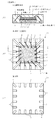
図6(A)は本実施の形態による半導体装置(半導体パッケージ)40の断面図、図6(B)はその平面図、図6(C)はその裏面図である。この半導体装置40は、半導体素子(ICチップ)1の裏面に予め接着剤42(又は接着テープ)等により接着したガラス、セラミックス等の絶縁基板41を半導体装置(又は封止材7)裏面に露出させ、かつリードフレームから作製された端子(外部端子)5の裏面及び側面を露出させ、絶縁基板41の裏面と端子5の裏面とを同一平面上に存在させた構造となっていることを特徴としている。その他は、図8に示した従来構造と同様である。
6A is a cross-sectional view of the semiconductor device (semiconductor package) 40 according to the present embodiment, FIG. 6B is a plan view thereof, and FIG. 6C is a rear view thereof. In this semiconductor device 40, an insulating substrate 41 made of glass, ceramics, or the like, which is bonded to the back surface of the semiconductor element (IC chip) 1 in advance with an adhesive 42 (or adhesive tape) or the like, is exposed on the back surface of the semiconductor device (or sealing material 7). And the back surface and the side surface of the terminal (external terminal) 5 manufactured from the lead frame are exposed so that the back surface of the insulating substrate 41 and the back surface of the
本実施の形態によれば、半導体ウェハの状態でその裏面にガラス等の絶縁基板41を被着した後は、図2(a)〜(f)に示した工程によって図6に示した半導体パッケージ40を作製する。従って、上述した第1の実施の形態と同様の作用効果を得ることができる。 According to the present embodiment, after the insulating substrate 41 such as glass is deposited on the back surface of the semiconductor wafer in the state of the semiconductor wafer, the semiconductor package shown in FIG. 6 is performed by the steps shown in FIGS. 40 is produced. Accordingly, it is possible to obtain the same operational effects as those of the first embodiment described above.
第4の実施の形態
図7は、本発明の第4の実施の形態を示すものである。
Fourth Embodiment FIG. 7 shows a fourth embodiment of the present invention.
図7(A)は本実施の形態による半導体装置(半導体パッケージ)50の断面図、図6(B)はその平面図、図6(C)はその裏面図である。この半導体装置50は、半導体素子(ICチップ)1の裏面に予め接着した片面接着テープ51を半導体装置(または封止材7)裏面に露出させ、かつリードフレームから作製された端子(外部端子)5の裏面及び側面を露出させ、片面接着テープ51の裏面と端子5の裏面とを同一平面上に存在させた構造となっていることを特徴としている。その他は、図8に示した従来構造と同様である。
7A is a sectional view of a semiconductor device (semiconductor package) 50 according to the present embodiment, FIG. 6B is a plan view thereof, and FIG. 6C is a rear view thereof. In this
本実施の形態によれば、半導体ウェハの状態でその裏面に片面接着テープ51を接着した後は、図2(a)〜(f)に示した工程によって図7に示した半導体パッケージ50を作製する。従って、上述した第1の実施の形態と同様の作用効果を得ることができる。上記の片面接着テープ51は、半導体素子1側に接着面を有し、ウェハ状態で接着されるものであるが、ダイシングシートに接着させたものや、ダイシングシート自体を用いることも可能である。
According to the present embodiment, after the single-sided adhesive tape 51 is bonded to the back surface of the semiconductor wafer in the state of the semiconductor wafer, the
以上に述べた各実施の形態は、本発明の技術的思想に基づいて種々に変形が可能である。 Each embodiment described above can be variously modified based on the technical idea of the present invention.
例えば、上述した半導体パッケージの各構成部分の材質や形状等は種々に変更してよいし、端子の配置やパターンも上述したものに限定されることはない。 For example, the material and shape of each component of the semiconductor package described above may be variously changed, and the terminal arrangement and pattern are not limited to those described above.
1…ICチップ(半導体素子)、2…電極パッド、3…ダイパッド、4…金属ワイヤ、5…端子(外部端子)、7…封止樹脂、8…ダイボンド材、
10、20、30、40、50…半導体パッケージ、21…絶縁性樹脂層、
23…はんだ、24…リードフレーム、25…樹脂フィルム、26…ブレード、
27…半導体ウェハ、28…プリント基板、29…接続ランド、31…絶縁膜、
41…絶縁基板、42…接着剤、51…片面接着テープ
DESCRIPTION OF
10, 20, 30, 40, 50 ... semiconductor package, 21 ... insulating resin layer,
23 ... solder, 24 ... lead frame, 25 ... resin film, 26 ... blade,
27 ... Semiconductor wafer, 28 ... Printed circuit board, 29 ... Connection land, 31 ... Insulating film,
41 ... Insulating substrate, 42 ... Adhesive, 51 ... Single-sided adhesive tape
Claims (10)
The insulating resin layer is formed on the back surface of the semiconductor wafer by spin coating, transfer molding, printing or potting, the insulating film is formed by sputtering or vapor deposition, the insulating substrate is bonded, and the single-sided adhesive tape is bonded. A method for manufacturing a semiconductor device according to claim 9.
Priority Applications (1)
| Application Number | Priority Date | Filing Date | Title |
|---|---|---|---|
| JP2004105834A JP2005294443A (en) | 2004-03-31 | 2004-03-31 | Semiconductor device and manufacturing method thereof |
Applications Claiming Priority (1)
| Application Number | Priority Date | Filing Date | Title |
|---|---|---|---|
| JP2004105834A JP2005294443A (en) | 2004-03-31 | 2004-03-31 | Semiconductor device and manufacturing method thereof |
Publications (1)
| Publication Number | Publication Date |
|---|---|
| JP2005294443A true JP2005294443A (en) | 2005-10-20 |
Family
ID=35327058
Family Applications (1)
| Application Number | Title | Priority Date | Filing Date |
|---|---|---|---|
| JP2004105834A Pending JP2005294443A (en) | 2004-03-31 | 2004-03-31 | Semiconductor device and manufacturing method thereof |
Country Status (1)
| Country | Link |
|---|---|
| JP (1) | JP2005294443A (en) |
Cited By (16)
| Publication number | Priority date | Publication date | Assignee | Title |
|---|---|---|---|---|
| WO2007052476A1 (en) * | 2005-11-02 | 2007-05-10 | Matsushita Electric Industrial Co., Ltd. | Electronic circuit device and method for manufacturing same |
| JP2009076658A (en) * | 2007-09-20 | 2009-04-09 | Renesas Technology Corp | Semiconductor device and manufacturing method thereof |
| JP2009253014A (en) * | 2008-04-07 | 2009-10-29 | Denso Corp | Method of manufacturing electronic device |
| JP2013038214A (en) * | 2011-08-08 | 2013-02-21 | Renesas Electronics Corp | Manufacturing method of semiconductor device |
| WO2013065895A1 (en) * | 2011-11-03 | 2013-05-10 | 주식회사 네패스 | Method for manufacturing a fanout semiconductor package using a lead frame, and semiconductor package and package-on-package for same |
| JP2013235999A (en) * | 2012-05-10 | 2013-11-21 | Renesas Electronics Corp | Manufacturing method of semiconductor device and semiconductor device |
| WO2014091714A1 (en) * | 2012-12-14 | 2014-06-19 | 旭化成エレクトロニクス株式会社 | Magnetic sensor and magnetic sensor device, and magnetic sensor manufacturing method |
| CN105185900A (en) * | 2014-06-17 | 2015-12-23 | 旭化成微电子株式会社 | Hall sensor |
| JP2016021549A (en) * | 2014-06-17 | 2016-02-04 | 旭化成エレクトロニクス株式会社 | Hall sensor |
| CN104170109B (en) * | 2012-12-14 | 2016-11-30 | 旭化成微电子株式会社 | Magnetic sensors and magnetic sensor devices |
| CN106686920A (en) * | 2016-12-23 | 2017-05-17 | 华中科技大学 | Method of increasing circuit stability |
| JP2018032852A (en) * | 2016-08-22 | 2018-03-01 | ローム株式会社 | Semiconductor device, and mounting structure for the same |
| JP2019220607A (en) * | 2018-06-21 | 2019-12-26 | 株式会社加藤電器製作所 | Method for manufacturing semiconductor device |
| CN111261595A (en) * | 2020-01-20 | 2020-06-09 | 上海艾为电子技术股份有限公司 | Base-island-free frame packaging structure and preparation method thereof |
| JP2020123641A (en) * | 2019-01-30 | 2020-08-13 | 新日本無線株式会社 | Semiconductor device and manufacturing method thereof |
| CN117238877A (en) * | 2023-11-14 | 2023-12-15 | 青岛泰睿思微电子有限公司 | DFN frame packaging structure and packaging method |
-
2004
- 2004-03-31 JP JP2004105834A patent/JP2005294443A/en active Pending
Cited By (31)
| Publication number | Priority date | Publication date | Assignee | Title |
|---|---|---|---|---|
| US7910406B2 (en) | 2005-11-02 | 2011-03-22 | Panasonic Corporation | Electronic circuit device and method for manufacturing same |
| WO2007052476A1 (en) * | 2005-11-02 | 2007-05-10 | Matsushita Electric Industrial Co., Ltd. | Electronic circuit device and method for manufacturing same |
| US8558362B2 (en) | 2007-09-20 | 2013-10-15 | Renesas Electronics Corporation | Semiconductor device and manufacturing method of the same |
| JP2009076658A (en) * | 2007-09-20 | 2009-04-09 | Renesas Technology Corp | Semiconductor device and manufacturing method thereof |
| JP2009253014A (en) * | 2008-04-07 | 2009-10-29 | Denso Corp | Method of manufacturing electronic device |
| JP2013038214A (en) * | 2011-08-08 | 2013-02-21 | Renesas Electronics Corp | Manufacturing method of semiconductor device |
| US8513060B2 (en) | 2011-08-08 | 2013-08-20 | Renesas Electronics Corporation | Manufacturing method using multi-step adhesive curing for sealed semiconductor device |
| US8941226B2 (en) | 2011-08-08 | 2015-01-27 | Renesas Electronics Corporation | Sealed semiconductor device having adhesive patch with inwardly sloped side surfaces |
| KR101297015B1 (en) | 2011-11-03 | 2013-08-14 | 주식회사 네패스 | Method of manufacturing fan-out semiconductor package using lead frame, semiconductor package thereof, and package on package thereof |
| WO2013065895A1 (en) * | 2011-11-03 | 2013-05-10 | 주식회사 네패스 | Method for manufacturing a fanout semiconductor package using a lead frame, and semiconductor package and package-on-package for same |
| JP2013235999A (en) * | 2012-05-10 | 2013-11-21 | Renesas Electronics Corp | Manufacturing method of semiconductor device and semiconductor device |
| US9269671B2 (en) | 2012-05-10 | 2016-02-23 | Renesas Electronics Corporation | Semiconductor device manufacturing method and semiconductor device |
| WO2014091714A1 (en) * | 2012-12-14 | 2014-06-19 | 旭化成エレクトロニクス株式会社 | Magnetic sensor and magnetic sensor device, and magnetic sensor manufacturing method |
| CN104170109A (en) * | 2012-12-14 | 2014-11-26 | 旭化成微电子株式会社 | Magnetic sensor, magnetic sensor device, and method for manufacturing magnetic sensor |
| CN106848055A (en) * | 2012-12-14 | 2017-06-13 | 旭化成微电子株式会社 | The manufacture method of Magnetic Sensor and magnet sensor arrangement and Magnetic Sensor |
| JPWO2014091714A1 (en) * | 2012-12-14 | 2017-01-05 | 旭化成エレクトロニクス株式会社 | Manufacturing method of magnetic sensor |
| CN104170109B (en) * | 2012-12-14 | 2016-11-30 | 旭化成微电子株式会社 | Magnetic sensors and magnetic sensor devices |
| JP2016021549A (en) * | 2014-06-17 | 2016-02-04 | 旭化成エレクトロニクス株式会社 | Hall sensor |
| JP2018137470A (en) * | 2014-06-17 | 2018-08-30 | 旭化成エレクトロニクス株式会社 | Hall sensor |
| CN105185900A (en) * | 2014-06-17 | 2015-12-23 | 旭化成微电子株式会社 | Hall sensor |
| JP2017120927A (en) * | 2014-06-17 | 2017-07-06 | 旭化成エレクトロニクス株式会社 | Hall sensor |
| CN107195772A (en) * | 2014-06-17 | 2017-09-22 | 旭化成微电子株式会社 | Hall sensor |
| CN107195772B (en) * | 2014-06-17 | 2019-06-25 | 旭化成微电子株式会社 | Hall sensor |
| CN105185900B (en) * | 2014-06-17 | 2018-07-06 | 旭化成微电子株式会社 | Hall sensor |
| JP2018032852A (en) * | 2016-08-22 | 2018-03-01 | ローム株式会社 | Semiconductor device, and mounting structure for the same |
| CN106686920A (en) * | 2016-12-23 | 2017-05-17 | 华中科技大学 | Method of increasing circuit stability |
| JP2019220607A (en) * | 2018-06-21 | 2019-12-26 | 株式会社加藤電器製作所 | Method for manufacturing semiconductor device |
| JP2020123641A (en) * | 2019-01-30 | 2020-08-13 | 新日本無線株式会社 | Semiconductor device and manufacturing method thereof |
| JP7243016B2 (en) | 2019-01-30 | 2023-03-22 | 日清紡マイクロデバイス株式会社 | Semiconductor device and its manufacturing method |
| CN111261595A (en) * | 2020-01-20 | 2020-06-09 | 上海艾为电子技术股份有限公司 | Base-island-free frame packaging structure and preparation method thereof |
| CN117238877A (en) * | 2023-11-14 | 2023-12-15 | 青岛泰睿思微电子有限公司 | DFN frame packaging structure and packaging method |
Similar Documents
| Publication | Publication Date | Title |
|---|---|---|
| US6441475B2 (en) | Chip scale surface mount package for semiconductor device and process of fabricating the same | |
| JP3461720B2 (en) | Resin-sealed semiconductor device | |
| JP5529371B2 (en) | Semiconductor device and manufacturing method thereof | |
| JP3189703B2 (en) | Semiconductor device and manufacturing method thereof | |
| US7405486B2 (en) | Circuit device | |
| JP5065586B2 (en) | Manufacturing method of semiconductor device | |
| JP2001015679A (en) | Semiconductor device and manufacturing method thereof | |
| JP2002026233A (en) | Semiconductor device and method of manufacturing the same | |
| JP2017147272A (en) | Semiconductor device and method for manufacturing the same, and lead frame intermediate used for manufacturing the semiconductor device | |
| US10943857B2 (en) | Substrate with multi-layer resin structure and semiconductor device including the substrate | |
| JP2005294443A (en) | Semiconductor device and manufacturing method thereof | |
| JP3660663B2 (en) | Chip package manufacturing method | |
| TWI834888B (en) | Package substrate | |
| KR101394647B1 (en) | Semiconductor package and method for fabricating the same | |
| JP2001332580A (en) | Semiconductor device and manufacturing method thereof | |
| JP2004063804A (en) | Semiconductor device, stacked semiconductor device, and method of manufacturing the same | |
| KR100831481B1 (en) | Semiconductor device and semiconductor package using the same, and circuit device | |
| JP4140012B2 (en) | Chip-shaped electronic component, manufacturing method thereof and mounting structure | |
| JP4881369B2 (en) | Manufacturing method of semiconductor device | |
| JP4356196B2 (en) | Semiconductor device assembly | |
| JP4311294B2 (en) | Electronic device and manufacturing method thereof | |
| JP2002124597A (en) | Method of making a plastic-enclosed component and a plastic-enclosed component | |
| JP4597183B2 (en) | Manufacturing method of semiconductor device | |
| JP2001127196A (en) | Terminal land frame and method of manufacturing the same, resin-encapsulated semiconductor device and method of manufacturing the same | |
| JP4179702B2 (en) | Manufacturing method of semiconductor device |