JP4597183B2 - Manufacturing method of semiconductor device - Google Patents
Manufacturing method of semiconductor device Download PDFInfo
- Publication number
- JP4597183B2 JP4597183B2 JP2007312675A JP2007312675A JP4597183B2 JP 4597183 B2 JP4597183 B2 JP 4597183B2 JP 2007312675 A JP2007312675 A JP 2007312675A JP 2007312675 A JP2007312675 A JP 2007312675A JP 4597183 B2 JP4597183 B2 JP 4597183B2
- Authority
- JP
- Japan
- Prior art keywords
- semiconductor chip
- semiconductor
- hole
- metal
- chips
- Prior art date
- Legal status (The legal status is an assumption and is not a legal conclusion. Google has not performed a legal analysis and makes no representation as to the accuracy of the status listed.)
- Expired - Lifetime
Links
Images


Classifications
-
- H—ELECTRICITY
- H01—ELECTRIC ELEMENTS
- H01L—SEMICONDUCTOR DEVICES NOT COVERED BY CLASS H10
- H01L2224/00—Indexing scheme for arrangements for connecting or disconnecting semiconductor or solid-state bodies and methods related thereto as covered by H01L24/00
- H01L2224/01—Means for bonding being attached to, or being formed on, the surface to be connected, e.g. chip-to-package, die-attach, "first-level" interconnects; Manufacturing methods related thereto
- H01L2224/10—Bump connectors; Manufacturing methods related thereto
- H01L2224/15—Structure, shape, material or disposition of the bump connectors after the connecting process
- H01L2224/16—Structure, shape, material or disposition of the bump connectors after the connecting process of an individual bump connector
- H01L2224/161—Disposition
- H01L2224/16135—Disposition the bump connector connecting between different semiconductor or solid-state bodies, i.e. chip-to-chip
- H01L2224/16145—Disposition the bump connector connecting between different semiconductor or solid-state bodies, i.e. chip-to-chip the bodies being stacked
-
- H—ELECTRICITY
- H01—ELECTRIC ELEMENTS
- H01L—SEMICONDUCTOR DEVICES NOT COVERED BY CLASS H10
- H01L2224/00—Indexing scheme for arrangements for connecting or disconnecting semiconductor or solid-state bodies and methods related thereto as covered by H01L24/00
- H01L2224/01—Means for bonding being attached to, or being formed on, the surface to be connected, e.g. chip-to-package, die-attach, "first-level" interconnects; Manufacturing methods related thereto
- H01L2224/42—Wire connectors; Manufacturing methods related thereto
- H01L2224/47—Structure, shape, material or disposition of the wire connectors after the connecting process
- H01L2224/48—Structure, shape, material or disposition of the wire connectors after the connecting process of an individual wire connector
- H01L2224/4805—Shape
- H01L2224/4809—Loop shape
- H01L2224/48091—Arched
-
- H—ELECTRICITY
- H01—ELECTRIC ELEMENTS
- H01L—SEMICONDUCTOR DEVICES NOT COVERED BY CLASS H10
- H01L2224/00—Indexing scheme for arrangements for connecting or disconnecting semiconductor or solid-state bodies and methods related thereto as covered by H01L24/00
- H01L2224/01—Means for bonding being attached to, or being formed on, the surface to be connected, e.g. chip-to-package, die-attach, "first-level" interconnects; Manufacturing methods related thereto
- H01L2224/42—Wire connectors; Manufacturing methods related thereto
- H01L2224/47—Structure, shape, material or disposition of the wire connectors after the connecting process
- H01L2224/48—Structure, shape, material or disposition of the wire connectors after the connecting process of an individual wire connector
- H01L2224/481—Disposition
- H01L2224/48151—Connecting between a semiconductor or solid-state body and an item not being a semiconductor or solid-state body, e.g. chip-to-substrate, chip-to-passive
- H01L2224/48221—Connecting between a semiconductor or solid-state body and an item not being a semiconductor or solid-state body, e.g. chip-to-substrate, chip-to-passive the body and the item being stacked
- H01L2224/48245—Connecting between a semiconductor or solid-state body and an item not being a semiconductor or solid-state body, e.g. chip-to-substrate, chip-to-passive the body and the item being stacked the item being metallic
- H01L2224/48247—Connecting between a semiconductor or solid-state body and an item not being a semiconductor or solid-state body, e.g. chip-to-substrate, chip-to-passive the body and the item being stacked the item being metallic connecting the wire to a bond pad of the item
-
- H—ELECTRICITY
- H01—ELECTRIC ELEMENTS
- H01L—SEMICONDUCTOR DEVICES NOT COVERED BY CLASS H10
- H01L2224/00—Indexing scheme for arrangements for connecting or disconnecting semiconductor or solid-state bodies and methods related thereto as covered by H01L24/00
- H01L2224/01—Means for bonding being attached to, or being formed on, the surface to be connected, e.g. chip-to-package, die-attach, "first-level" interconnects; Manufacturing methods related thereto
- H01L2224/42—Wire connectors; Manufacturing methods related thereto
- H01L2224/47—Structure, shape, material or disposition of the wire connectors after the connecting process
- H01L2224/48—Structure, shape, material or disposition of the wire connectors after the connecting process of an individual wire connector
- H01L2224/484—Connecting portions
- H01L2224/48463—Connecting portions the connecting portion on the bonding area of the semiconductor or solid-state body being a ball bond
- H01L2224/48465—Connecting portions the connecting portion on the bonding area of the semiconductor or solid-state body being a ball bond the other connecting portion not on the bonding area being a wedge bond, i.e. ball-to-wedge, regular stitch
-
- H—ELECTRICITY
- H01—ELECTRIC ELEMENTS
- H01L—SEMICONDUCTOR DEVICES NOT COVERED BY CLASS H10
- H01L2924/00—Indexing scheme for arrangements or methods for connecting or disconnecting semiconductor or solid-state bodies as covered by H01L24/00
- H01L2924/01—Chemical elements
- H01L2924/01078—Platinum [Pt]
Abstract
Description
この発明は、LSIを有する半導体チップを積層し、かつ電気的に接続された半導体装置の製造方法に関するものである。 The present invention relates to a method of manufacturing a semiconductor device in which semiconductor chips having LSIs are stacked and electrically connected.
近年、LSI半導体装置の低コスト化及び小型化を図るために、互いに異なる機能を有するLSI又は互いに異なるプロセスにより形成されたLSIを有する半導体チップ同士がフェイスダウン方式で接合されてなる半導体装置が提案されている。 In recent years, in order to reduce the cost and size of LSI semiconductor devices, semiconductor devices in which semiconductor chips having LSIs having different functions or LSIs formed by different processes are joined together in a face-down manner have been proposed. Has been.
以下、前記従来のLSI半導体装置について図16を参照しながら説明する。まず、第1の半導体チップ110の上に第1の半導体チップの内部電極(第1の内部電極)111及びボンディングパッド112が、また第1の内部電極111上に第1の半導体チップのバリヤメタル(第1のバリヤメタル)113が形成されているとともに、第2の半導体チップの内部電極(第2の内部電極)121上の第2の半導体チップのバリヤメタル(第2のバリヤメタル)122とはんだよりなるバンプ123を介して第2の半導体チップ120の上の第2の内部電極121と互いに電気的に接続されている。また第1の半導体チップ110と第2の半導体チップ120との間には絶縁性樹脂130が充填されており、第1の半導体チップ110と第2の半導体チップ120とはバンプ123及び絶縁性樹脂130によって一体化されている。
The conventional LSI semiconductor device will be described below with reference to FIG. First, the internal electrode (first internal electrode) 111 and the
第1の半導体チップ110はリードフレームのダイパッド131にダイボンド樹脂132により固定されているとともに、第1の半導体チップ110のボンディングパッド112とリードフレームの外部リード133とはボンディングワイヤ134を介して電気的に接続されている。第1の半導体チップ110、第2の半導体チップ120、ボンディングワイヤ133、ダイパッド131及び外部リード133の一部は封止用樹脂135によってパッケージされている。
The
以下、前記の半導体装置製造方法について、図17を参照しながら説明する。まず、図17(a)に示すように、第2の半導体チップ120の内部電極121に電解めっき法によりはんだバンプ123を形成する。はんだのバンプ123の形成については、第2の半導体チップ120のウエハ上に蒸着により第2のバリヤメタル122を形成した後、レジストによりバンプパターンを形成し電解はんだめっきによりバンプ123を形成する。次にはんだバンプ123をマスクにして第2のバリヤメタル122をウエットエッチングにより溶解除去した後、はんだバンプ123をリフローして半球状にする。次に図17(b)に示すように、第1の半導体チップ110がウエハ状態の時に、第1の半導体チップ110上に絶縁樹脂130を塗布し、第2の半導体チップ120のはんだバンプ123と第1の半導体チップ110の内部電極111を一致させる。次に図17(c)に示すように、第2の半導体チップ120を第1の半導体チップ110に設置する。その後、加熱によりはんだバンプ122を溶融させ第2の半導体チップ120の内部電極121と第1の半導体チップ110の内部電極111をはんだづけにより接合する。次に図17(d)に示すように、第1の半導体チップ110をウエハ状態から個別に、分割する。最後に図16に示すように、第1の半導体チップ110をリードフレームのダイパッド131にダイボンドし、第1の半導体チップ110のボンディングパッド112とリードフレームの外部リード132をワイヤボンディングにより接続し、封止用樹脂135によってパッケージしている。
しかしながら、前記従来の半導体装置の構造および製造方法によると、第1の半導体チップと第2の半導体チップの接続をはんだバンプを用いたはんだ付けであるため、次に示す課題があった。 However, according to the structure and manufacturing method of the conventional semiconductor device, since the connection between the first semiconductor chip and the second semiconductor chip is soldering using solder bumps, there are the following problems.
(1)第1の半導体チップをフェイスダウン方式で第2の半導体チップに積層するため、チップを2段までしか積層する事が出来なかった。 (1) Since the first semiconductor chip is stacked on the second semiconductor chip by the face-down method, the chip can be stacked only up to two stages.
(2)第1の半導体チップを第2の半導体チップに積層する際に、金属バンプを使用するために、チップにダメージを与え半導体素子を破壊することがあった。 (2) When the first semiconductor chip is stacked on the second semiconductor chip, the metal bumps are used, so that the chip may be damaged and the semiconductor element may be destroyed.
(3)接合時にはんだが溶融するためはんだバンプが横方向に広がる寸法変化が生じ微細化が困難であった。 (3) Since the solder melts at the time of joining, a dimensional change in which the solder bump spreads in the lateral direction occurs, and miniaturization is difficult.
(4)通常、半導体チップの内部電極はAlであるため、はんだ接合のためには、Al電極上にはんだと容易に拡散する金属膜、例えば、Ti−Cu−Au等を形成しておく必要があり、コストの高いものである。 (4) Since the internal electrode of the semiconductor chip is usually Al, a metal film that easily diffuses with the solder, for example, Ti—Cu—Au or the like, must be formed on the Al electrode for solder bonding. There is a high cost.
(5)微細化が困難であるため、第1及び第2の半導体チップの内部電極が大きいため電気的な負荷容量が大きくなり、第1の半導体チップと第2の半導体チップ間の信号伝送において、遅延が大きくかつ電力消費の大きいものである。 (5) Since the miniaturization is difficult and the internal electrodes of the first and second semiconductor chips are large, the electrical load capacity increases, and in signal transmission between the first semiconductor chip and the second semiconductor chip. The delay is large and the power consumption is large.
したがって、この発明の目的は、前記の問題を解消するものであり、チップにダメージを与えず、しかも多数枚のチップの積層することができ、微細な接続を容易にした高性能な半導体装置の製造方法を提供することである。 Accordingly, an object of the present invention is to solve the above-described problems, and to provide a high-performance semiconductor device that can stack a large number of chips without damaging the chips and facilitates fine connection. It is to provide a manufacturing method.
上記課題を解決するために、本発明の第1の半導体装置の製造方法は、第1の半導体チップに積層される第2の半導体チップの内部電極に前記第2の半導体チップを貫通する貫通孔を設ける工程と、前記貫通孔内壁および裏面に絶縁膜を形成する工程と、前記貫通孔内壁に第1の金属を無電解めっきまたは蒸着により形成する工程と、前記第1および第2の半導体チップの内部電極同士が対応するように、前記第1の半導体チップに対して間隙を有した状態で前記第2の半導体チップを前記第1の半導体チップの外部電極および内部電極を除く部分に接着固定する工程と、前記第2の半導体チップの内部電極および貫通孔内壁の前記第1の金属と前記第1の半導体チップの内部電極を無電解めっきにより電気的に接続する工程とを含む。 In order to solve the above-described problem, a first method for manufacturing a semiconductor device according to the present invention includes a through-hole penetrating the second semiconductor chip in an internal electrode of a second semiconductor chip stacked on the first semiconductor chip. A step of forming an insulating film on the inner wall and the back surface of the through hole, a step of forming a first metal on the inner wall of the through hole by electroless plating or vapor deposition, and the first and second semiconductor chips. The second semiconductor chip is bonded and fixed to a portion of the first semiconductor chip excluding the external electrode and the internal electrode in a state having a gap with respect to the first semiconductor chip so that the internal electrodes correspond to each other. And a step of electrically connecting the internal electrode of the second semiconductor chip and the first metal of the inner wall of the through hole to the internal electrode of the first semiconductor chip by electroless plating.
このように、第2の半導体チップの内部電極内に貫通孔を設け、第1および第2の半導体チップを接着固定し、第2の半導体チップの内部電極および貫通孔内壁の第1の金属と第1の半導体チップの内部電極を無電解めっきにより電気的に接続するので、多数枚のチップをチップへダメージを与えることなしに積層することが可能となる。また、貫通孔内壁に無電解めっきが可能な第1の金属を無電解めっきまたは蒸着により形成するので、従来のようなはんだバンプによる接合ではなく、チップの内部電極上に予めはんだの拡散が生じる金属の形成も不要となる。第1の金属として、例えばCu,Ni,Au,Pt,Ag,Sn,Pb,Co等を用いることができる。また、はんだバンプが広がることがないため、微細な接続が容易になり、多ピンLSIへの適用が可能となる。また、LSIチップ同士の接合を片側のLSIは、ウエハ状態で行うことにより、低コスト化が可能となる。 As described above, the through hole is provided in the internal electrode of the second semiconductor chip, the first and second semiconductor chips are bonded and fixed, and the internal electrode of the second semiconductor chip and the first metal on the inner wall of the through hole are Since the internal electrodes of the first semiconductor chip are electrically connected by electroless plating, a large number of chips can be stacked without damaging the chips. In addition, since the first metal capable of electroless plating is formed on the inner wall of the through hole by electroless plating or vapor deposition, solder diffusion occurs in advance on the internal electrode of the chip instead of the conventional solder bump bonding. Metal formation is also unnecessary. For example, Cu, Ni, Au, Pt, Ag, Sn, Pb, Co or the like can be used as the first metal. Further, since solder bumps do not spread, fine connection is facilitated, and application to a multi-pin LSI becomes possible. In addition, the LSIs on one side can be bonded to each other in the wafer state, so that the cost can be reduced.
本発明の第2の半導体装置の製造方法は、第1の半導体チップに積層される第2の半導体チップの内部電極に前記第2の半導体チップを貫通する貫通孔を設ける工程と、前記貫通孔内壁および裏面に絶縁膜を形成する工程と、前記貫通孔内壁に第1の金属を無電解めっきまたは蒸着により形成する工程と、前記第1および第2の半導体チップの内部電極同士が対応するように、前記第1の半導体チップに対して間隙を有した状態で前記第2の半導体チップを前記第1の半導体チップの外部電極および内部電極を除く部分に接着固定する工程と、前記第2の半導体チップ上にさらに1個以上の第2の半導体チップを下層および上層の第2の半導体チップの内部電極同士が対応するように配置し、前記下層の第2の半導体チップに対して前記上層の第2の半導体チップが間隙を有した状態で前記上層の第2の半導体チップを前記下層の第2の半導体チップの内部電極を除く部分に接着固定する工程と、前記第2の半導体チップの内部電極および貫通孔内壁の前記第1の金属と前記第1の半導体チップの内部電極を無電解めっきにより電気的に接続する工程とを含む。 According to a second method of manufacturing a semiconductor device of the present invention, a step of providing a through hole penetrating the second semiconductor chip in an internal electrode of a second semiconductor chip stacked on the first semiconductor chip, and the through hole The step of forming an insulating film on the inner wall and the back surface, the step of forming the first metal on the inner wall of the through hole by electroless plating or vapor deposition, and the inner electrodes of the first and second semiconductor chips correspond to each other. And a step of adhering and fixing the second semiconductor chip to a portion of the first semiconductor chip excluding the external electrode and the internal electrode in a state having a gap with respect to the first semiconductor chip; One or more second semiconductor chips are further arranged on the semiconductor chip so that the internal electrodes of the lower and upper second semiconductor chips correspond to each other, and the upper layer with respect to the lower second semiconductor chip. A step of adhering and fixing the second semiconductor chip in the upper layer to a portion excluding an internal electrode of the second semiconductor chip in the lower layer in a state where the second semiconductor chip has a gap; and the inside of the second semiconductor chip Electrically connecting the first metal of the electrode and the inner wall of the through hole and the internal electrode of the first semiconductor chip by electroless plating.
この構成によると、第1の発明と同様の作用効果を有する。 According to this structure, it has the same effect as 1st invention.
上記第1および第2の半導体装置の製造方法においては、前記貫通孔内壁に記第1の金属としてCu,Ni,Au,Pt,Ag,Sn等を形成する工程を有することが好ましい。 The first and second semiconductor device manufacturing methods preferably include a step of forming Cu, Ni, Au, Pt, Ag, Sn or the like as the first metal on the inner wall of the through hole.
また、上記第1および第2の半導体装置の製造方法においては、前記第2の半導体チップの内部電極および貫通孔内壁の前記第1の金属と前記第1の半導体チップの内部電極を無電解めっきにより電気的に接続する工程において、無電解めっきによりNiあるいはAuをめっきすることが好ましい。 In the first and second semiconductor device manufacturing methods, the internal electrode of the second semiconductor chip, the first metal on the inner wall of the through hole, and the internal electrode of the first semiconductor chip are electrolessly plated. In the step of electrically connecting with Ni, it is preferable to plate Ni or Au by electroless plating.
本発明の半導体装置の製造方法によれば、第2の半導体チップの内部電極内に貫通孔を設け、第1および第2の半導体チップを接着固定し、第2の半導体チップの内部電極および貫通孔内壁の第1の金属と第1の半導体チップの内部電極を無電解めっきにより電気的に接続するので、多数枚のチップをチップへダメージを与えることなしに積層することが可能となる。また、貫通孔内壁に無電解めっきが可能な第1の金属を無電解めっきまたは蒸着により形成するので、従来のようなはんだバンプによる接合ではなく、チップの内部電極上に予めはんだの拡散が生じる金属の形成も不要となる。第1の金属として、例えばCu,Ni,Au,Pt,Ag,Sn,Pb,Co等を用いることができる。また、はんだバンプが広がることがないため、微細な接続が容易になり、多ピンLSIへの適用が可能となる。また、LSIチップ同士の接合を片側のLSIは、ウエハ状態で行うことにより、低コスト化が可能となる。 According to the method for manufacturing a semiconductor device of the present invention, a through hole is provided in the internal electrode of the second semiconductor chip, the first and second semiconductor chips are bonded and fixed, and the internal electrode and the through hole of the second semiconductor chip are bonded. Since the first metal on the inner wall of the hole and the internal electrode of the first semiconductor chip are electrically connected by electroless plating, it is possible to stack a large number of chips without damaging the chips. In addition, since the first metal capable of electroless plating is formed on the inner wall of the through hole by electroless plating or vapor deposition, solder diffusion occurs in advance on the internal electrode of the chip instead of the conventional solder bump bonding. Metal formation is also unnecessary. For example, Cu, Ni, Au, Pt, Ag, Sn, Pb, Co or the like can be used as the first metal. Further, since solder bumps do not spread, fine connection is facilitated, and application to a multi-pin LSI becomes possible. In addition, the LSIs on one side can be bonded to each other in the wafer state, so that the cost can be reduced.
この発明の実施の形態を図1〜図15に基づいて説明する。図1はこの発明の実施の形態の半導体装置の断面図、図2は図1の要部拡大図、図3〜図15はこの発明の実施の形態の半導体装置の製造方法を示す工程別断面図である。 An embodiment of the present invention will be described with reference to FIGS. 1 is a cross-sectional view of a semiconductor device according to an embodiment of the present invention, FIG. 2 is an enlarged view of a main part of FIG. 1, and FIGS. 3 to 15 are cross-sectional views showing a method of manufacturing a semiconductor device according to an embodiment of the present invention. FIG.
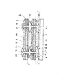
図1および図2において、1は第1の半導体チップ、2は半導体チップの保護膜、3は第1の半導体チップの外部電極、4は第1の半導体チップの内部電極、5は接着剤、6は貫通孔、7は第2の半導体チップ、8は第2の半導体チップの内部電極、9は第3の半導体チップ、10は第3の半導体チップの内部電極、11は第2の半導体チップの酸化膜、12は第3の半導体チップの酸化膜、13は第2の半導体チップのめっき電極(第2のめっき電極)、14は第3の半導体チップのめっき電極(第3のめっき電極)、15はめっき電極(第2の金属)、16はダイボンド樹脂、17はリードフレームのリード、18はリードフレームのダイパッド、19はボンディングワイヤ、20は封止樹脂、21は第2の半導体チップよりなるウエハ、22は第3の半導体チップよりなるウエハ、23は無電解めっき液、24は無電解めっき槽、25はめっき金属膜(第1の金属)、26はレジスト、27はエッチング液、28はエッチング槽、29は第1の半導体チップのウエハ、30はコレット、31はコレットの真空孔、32はダイシングの溝、33は絶縁樹脂、34は酸化膜を示している。 1 and 2, 1 is a first semiconductor chip, 2 is a protective film of the semiconductor chip, 3 is an external electrode of the first semiconductor chip, 4 is an internal electrode of the first semiconductor chip, 5 is an adhesive, 6 is a through hole, 7 is a second semiconductor chip, 8 is an internal electrode of the second semiconductor chip, 9 is a third semiconductor chip, 10 is an internal electrode of the third semiconductor chip, and 11 is a second semiconductor chip. Oxide film, 12 is an oxide film of the third semiconductor chip, 13 is a plating electrode (second plating electrode) of the second semiconductor chip, and 14 is a plating electrode (third plating electrode) of the third semiconductor chip. , 15 is a plating electrode (second metal), 16 is a die bond resin, 17 is a lead frame lead, 18 is a lead frame die pad, 19 is a bonding wire, 20 is a sealing resin, and 21 is a second semiconductor chip. Wafer 22 is a wafer made of a third semiconductor chip, 23 is an electroless plating solution, 24 is an electroless plating bath, 25 is a plating metal film (first metal), 26 is a resist, 27 is an etching solution, and 28 is an etching bath. , 29 are first semiconductor chip wafers, 30 are collets, 31 are collet vacuum holes, 32 are dicing grooves, 33 are insulating resins, and 34 is an oxide film.
図1に示すように、外部電極3と内部電極4を有する第1の半導体チップ1と第2,3の半導体チップ7,9は間隙を有した状態で、外部電極3及び内部電極4,8,10を除く部分で接着剤5によって固定されている。また、第2,3の半導体チップ7,9は第2,3の半導体チップの内部電極8,10内に半導体チップの裏面までの貫通孔6を有し、貫通孔6および第2,3の半導体チップ7,9の裏面には第2,3の半導体チップの酸化膜11,12が形成され、内部素子との絶縁を保っている。貫通孔内壁には無電解めっきが可能なめっき金属膜25であるCu,Ni,Au,Pt,Ag,Sn,Pb,Co等が形成してある。そして、第2,3の半導体チップの内部電極8,10および貫通孔6と第1の半導体チップの内部電極4が同一組成の連続しためっき電極15により電気的に接続されている。
As shown in FIG. 1, the
次に、上記構成の半導体装置の製造方法について説明する。図3〜図9、図14において、(b)は(a)の拡大図である。まず始めに、図3(a),(b)に示すように第2,3の半導体チップよりなるウエハ21,22の第2,3の半導体チップの内部電極8,10にレーザにより直径が10μm程度の貫通孔6を開ける。内部電極サイズは、15μm□以上あれはよい。次に図4(a),(b)に示すように、貫通孔6の側面および第2,3の半導体チップよりなるウエハ21,22の裏面に第2,3の半導体チップの酸化膜11,12を形成する。この酸化膜11,12は無電解めっき法により電極を形成した際の、半導体チップの内部素子との絶縁膜となる。
Next, a method for manufacturing the semiconductor device having the above configuration will be described. 3 to 9 and 14, (b) is an enlarged view of (a). First, as shown in FIGS. 3A and 3B, the
次に図5(a),(b)に示すように、第2,3の半導体チップよりなるウエハ21,22と貫通孔6に無電解めっきによりウエハ全面にめっき金属膜25を形成する。例えは、無電解めっきで形成するめっき金属膜25がNiである場合は、塩化パラジウムの溶液に第2,3の半導体チップよりなるウエハ21,22を浸漬しウエハ全面に無電解めっき核としてパラジウムを付着した後に無電解Niめっき液に浸漬することでNiのめっき金属膜25を1μm程度の膜厚を形成する。次に図6(a),(b)に示すように、第2,3の半導体チップよりなるウエハ21,22の第2,3の半導体チップの内部電極8,10と貫通孔6に、レジスト26によりめっき金属膜25を除去するための、エッチングパターンを形成する。
Next, as shown in FIGS. 5A and 5B, a plated
次に図7(a),(b)に示すように、レジスト26でエッチングパターンを形成した第2,3の半導体チップよりなるウエハ21,22をエッチング槽28中のエッチング液27に浸漬し、めっき金属膜25を溶解エッチングする。例えは、めっき金属膜がNiである場合は20%の塩酸溶液によりNi膜を溶解する。次に図8(a),(b)に示すように、第2,3の半導体チップよりなるウエハ21,22に形成したレジスト26を溶解除去して、第2,3のめっき電極13,14が形成される。次に図9(a),(b)に示すように、第2,3の半導体チップよりなるウエハ21,22をダイシングし、個々のチップに分割する。
Next, as shown in FIGS. 7A and 7B, the wafers 21 and 22 made of the second and third semiconductor chips in which the etching pattern is formed by the resist 26 are immersed in the
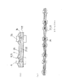
次に図10に示すように、第1の半導体チップ1よりなる半導体ウエハ29の、後に第2の半導体チップ7を搭載する位置で第1の半導体チップの内部電極4及び、外部電極3をふさがないようにエポキシ、ポリイミド、アクリル等の接着剤5を塗布する。次に図11に示すように、第2の半導体チップ7を第1の半導体チップよりなるウエハ29の接着剤5を塗布した領域に、内部電極4,8同士が一致するようにコレット30にて真空吸着した状態でフェースアップにて設置する。その後コレット30を介して加熱することにより接着剤5を硬化し第2の半導体チップ7を第1の半導体チップよりなるウエハ29上に固定する。加熱温度は100℃〜300℃程度である。内部電極4,8の大きさは、第2の半導体チップ7と第1の半導体チップよりなるウエハ29を接続するための電極であるため小さくてよく数μm□〜100μm□程度である。また、この時、第1の半導体チップ1と第2の半導体チップ7の表面間の間隙は、数μmから100μmである。また、接着剤5は、内部電極4,8の表面には流れないようにしておく。この工程を繰り返すことにより第1の半導体チップよりなるウエハ29上に複数個の第2の半導体チップ7を接着剤5により固定する。
Next, as shown in FIG. 10, the
さらに図12に示すように、第2の半導体チップ7上に後に第3の半導体チップ9を搭載する位置で内部電極8をふさがないようにエポキシ、ポリイミド、アクリル等の接着剤5を塗布する。次に図13に示すように、第3の半導体チップ9を第2の半導体チップ7の接着剤5を塗布した領域に、内部電極8,10同士が一致するようにコレット30にて真空吸着した状態でフェースアップにて設置する。その後コレット30を介して加熱することにより接着剤5を硬化し第3の半導体チップ9を第2の半導体チップ7上に固定する。
Further, as shown in FIG. 12, an adhesive 5 such as epoxy, polyimide, acrylic or the like is applied on the
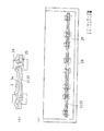
次に図14(a),(b)に示すように、第1の半導体チップよりなるウエハ29を無電解めっき漕24に浸漬することで、第1の半導体チップの内部電極4と第2,3の半導体チップの内部電極8,10に形成した第2,3のめっき電極13,14から析出しためっき金属は一体となりめっき電極15を形成する。めっき電極15により第1の半導体チップ1の内部電極4と第2,3の半導体チップ7,9の内部電極8,10が電気的に接続される。この時、第1の半導体チップよりなるウエハ29と第2,3の半導体チップ7,9の間隙および貫通孔6に無電解めっき液23が浸入する。例えば第1の半導体チップの内部電極4がAlで後に行う無電解めっきで析出させる金属がNiの場合は、まず、硝酸、燐酸等の溶液に浸漬し、第1の半導体チップの内部電極4のAl表面の酸化膜を除去した後、Al表面を亜鉛等で置換する。また、第2,3の半導体チップ7,9に形成した第2,3のめっき電極13,14と同一の無電解めっき液を使用することで、第2,3のめっき電極13,14上にも無電解めっきの金属が析出し、第1,2,3の半導体チップの内部電極4,8,10を同一のめっき金属で接続できる。この時、めっき金属Niの表面にさらに金を無電解めっきすることにより信頼性を向上させることができるとともに、後に外部電極4上にボンディングワイヤ等を接合するときに大変歩留まりの高いものとなる。それぞれの溶液に浸漬し処理した後は、純水等の溶液で洗浄した後に次の処理を実施する。このように、従来のようなはんだバンプによる接合ではなく、Al電極に直接無電解めっきで析出させる金属で接合するため、従来のようにAl電極上にあらかじめはんだの拡散が生じる金属の形成も不要となるとともに、ウエハ状態で全てのチップの接合を一括で接合できるため、飛躍的に生産性が向上し、低コストで高密度の接続を実現することができる。
Next, as shown in FIGS. 14A and 14B, by immersing the
次に図15に示すように、第1の半導体チップよりなるウエハ29をダイシングし第1の半導体チップ1に分離する。ここで、第1の半導体チップ1に分離する前に第1の半導体チップの外部電極3にプロービングし、第1の半導体チップ1と第2の半導体チップ7と第3の半導体チップ9が接合された状態で特性検査を行うことができる。また、絶縁樹脂33を側部に設ける。
Next, as shown in FIG. 15, the
次に、図1および図2に示すように、第2,3の半導体チップ7、9が接合された第1の半導体チップ1をリードフレームのダイパッド18にダイボンド樹脂16に接着し、第1の外部電極3とリードフレームのリード17をボンディングワイヤ19にて接続し、最後に封止樹脂20にて封止することによりパッケージングする。この時、封止樹脂20は、金型への樹脂注入時に第1の半導体チップ1と第2の半導体チップ7と第3の半導体チップ9の間隙にまで注入される。また、第1の半導体チップ1と第2の半導体チップ7と第3の半導体チップ9の間隙への樹脂注入は、パッケージの封止樹脂とは異なる絶縁性樹脂16で封止する前に行ってもかまわない。また、封止樹脂が第1の半導体チップ1と第2の半導体チップ7と第3の半導体チップ9の間隙には、樹脂が注入されない状態としてもかまわない。また、積層する半導体チップにおいては、第1の半導体チップに対して内部電極の位置関係が回路上問題がなければ、フェイスアップとフェイスダウンのどちらでもよい。
Next, as shown in FIGS. 1 and 2, the
以上のようにこの実施の形態によれば、第2,3の半導体チップの内部電極8,10内に貫通孔6を設け、第1および第2,3の半導体チップ1,7,9を接着固定し、第2,3の半導体チップの内部電極8,10および貫通孔内壁の第1の金属25と第1の半導体チップの内部電極4を無電解めっきにより電気的に接続するので、多数枚のチップをチップへダメージを与えることなしに積層することが可能となる。また、貫通孔内壁に無電解めっきが可能な第1の金属25を無電解めっきまたは蒸着により形成するので、従来のようなはんだバンプによる接合ではなく、チップの内部電極上に予めはんだの拡散が生じる金属の形成も不要となる。第1の金属25として、例えばCu,Ni,Au,Pt,Ag,Sn,Pb,Co等を用いることができる。また、はんだバンプが広がることがないため、微細な接続が容易になり、多ピンLSIへの適用が可能となる。また、LSIチップ同士の接合を片側のLSIは、ウエハ状態で行うことにより、低コスト化が可能となる。
As described above, according to this embodiment, the through-
また、第2の半導体チップの内部電極8内の貫通孔6の径が、第1の半導体チップ1と第2の半導体チップ7との間隙の1/2よりも小さくしてもよい。すなわち、図2において、aは第2の半導体チップの内部電極内の貫通孔の径、bは第1の半導体チップと第2の半導体チップとの間隙である。a>b/2のとき、貫通孔6がめっき金属(めっき電極15)で埋まる前に、他の電極より成長しためっき金属(第2の半導体チップのめっき電極13等)と接触するため、貫通孔6内部にめっき液が残る。a≦b/2のとき、他の電極より成長しためっき金属と接触する前に貫通孔6がめっき金属で埋まってしまう。このため、確実に接続できる。
Further, the diameter of the through
なお、第2,3の半導体チップを積層した場合を示したが、第2の半導体チップを2チップ以上積層してもよい。また、第2の半導体チップが接続される第1の半導体チップは、ウエハの状態の他、回路基板として構成してもよい。 Although the case where the second and third semiconductor chips are stacked is shown, two or more second semiconductor chips may be stacked. Further, the first semiconductor chip to which the second semiconductor chip is connected may be configured as a circuit board in addition to the wafer state.
本発明にかかる半導体装置の製造方法は、多数枚のチップをチップへダメージを与えることなしに積層することが可能となるという効果を有し、半導体製造等に有用である。 The method for manufacturing a semiconductor device according to the present invention has an effect that a large number of chips can be stacked without damaging the chips, and is useful for semiconductor manufacturing and the like.
1 第1の半導体チップ
2 半導体チップの保護膜
3 第1の半導体チップの外部電極
4 第1の半導体チップの内部電極
5 接着剤
6 貫通孔
7 第2の半導体チップ
8 第2の半導体チップの内部電極
9 第3のチップ
10 第3のチップの内部電極
11 第2の半導体チップの酸化膜
12 第3の半導体チップの酸化膜
13 第2のめっき電極
14 第3のめっき電極
15 めっき電極
16 ダイボンド樹脂
17 リードフレームのリード
18 リードフレームのダイパッド
19 ボンディングワイヤ
20 封止樹脂
21 第2の半導体チップよりなるウエハ
22 第3の半導体チップよりなるウエハ
23 無電解めっき液
24 無電解めっき槽
25 めっき金属膜
26 レジスト
27 エッチング液
28 エッチング槽
29 第1の半導体チップのウエハ
30 コレット
31 コレットの真空孔
32 ダイシングの溝
33 絶縁樹脂
34 酸化膜
DESCRIPTION OF
Claims (4)
前記貫通孔内壁および裏面に絶縁膜を形成する工程と、
前記貫通孔内壁に第1の金属を無電解めっきまたは蒸着により形成する工程と、
前記第1および第2の半導体チップの内部電極同士が対応するように、前記第1の半導体チップに対して間隙を有した状態で前記第2の半導体チップを前記第1の半導体チップの外部電極および内部電極を除く部分に接着固定する工程と、
前記第2の半導体チップの内部電極および貫通孔内壁の前記第1の金属と前記第1の半導体チップの内部電極を無電解めっきにより電気的に接続する工程とを含む半導体装置の製造方法。 Providing a through hole penetrating the second semiconductor chip in an internal electrode of the second semiconductor chip stacked on the first semiconductor chip;
Forming an insulating film on the inner wall and the back surface of the through hole;
Forming a first metal on the inner wall of the through hole by electroless plating or vapor deposition;
The second semiconductor chip is connected to the external electrode of the first semiconductor chip with a gap with respect to the first semiconductor chip so that the internal electrodes of the first and second semiconductor chips correspond to each other. And a step of adhering and fixing to a portion excluding the internal electrode,
A method of manufacturing a semiconductor device, comprising: electrically connecting the internal electrode of the second semiconductor chip and the first metal of the inner wall of the through hole to the internal electrode of the first semiconductor chip by electroless plating.
前記貫通孔内壁および裏面に絶縁膜を形成する工程と、
前記貫通孔内壁に第1の金属を無電解めっきまたは蒸着により形成する工程と、
前記第1および第2の半導体チップの内部電極同士が対応するように、前記第1の半導体チップに対して間隙を有した状態で前記第2の半導体チップを前記第1の半導体チップの外部電極および内部電極を除く部分に接着固定する工程と、
前記第2の半導体チップ上にさらに1個以上の第2の半導体チップを下層および上層の第2の半導体チップの内部電極同士が対応するように配置し、前記下層の第2の半導体チップに対して前記上層の第2の半導体チップが間隙を有した状態で前記上層の第2の半導体チップを前記下層の第2の半導体チップの内部電極を除く部分に接着固定する工程と、
前記第2の半導体チップの内部電極および貫通孔内壁の前記第1の金属と前記第1の半導体チップの内部電極を無電解めっきにより電気的に接続する工程とを含む半導体装置の製造方法。 Providing a through hole penetrating the second semiconductor chip in an internal electrode of the second semiconductor chip stacked on the first semiconductor chip;
Forming an insulating film on the inner wall and the back surface of the through hole;
Forming a first metal on the inner wall of the through hole by electroless plating or vapor deposition;
The second semiconductor chip is connected to the external electrode of the first semiconductor chip with a gap with respect to the first semiconductor chip so that the internal electrodes of the first and second semiconductor chips correspond to each other. And a step of adhering and fixing to a portion excluding the internal electrode,
One or more second semiconductor chips are further arranged on the second semiconductor chip so that the internal electrodes of the lower and upper second semiconductor chips correspond to each other, and the second semiconductor chip is lower than the second semiconductor chip. Bonding and fixing the upper second semiconductor chip to a portion excluding the internal electrode of the lower second semiconductor chip in a state where the upper second semiconductor chip has a gap;
A method of manufacturing a semiconductor device, comprising: electrically connecting the internal electrode of the second semiconductor chip and the first metal of the inner wall of the through hole to the internal electrode of the first semiconductor chip by electroless plating.
Priority Applications (1)
| Application Number | Priority Date | Filing Date | Title |
|---|---|---|---|
| JP2007312675A JP4597183B2 (en) | 2007-12-03 | 2007-12-03 | Manufacturing method of semiconductor device |
Applications Claiming Priority (1)
| Application Number | Priority Date | Filing Date | Title |
|---|---|---|---|
| JP2007312675A JP4597183B2 (en) | 2007-12-03 | 2007-12-03 | Manufacturing method of semiconductor device |
Related Parent Applications (1)
| Application Number | Title | Priority Date | Filing Date |
|---|---|---|---|
| JP31222299A Division JP4245754B2 (en) | 1999-11-02 | 1999-11-02 | Semiconductor device |
Publications (2)
| Publication Number | Publication Date |
|---|---|
| JP2008072150A JP2008072150A (en) | 2008-03-27 |
| JP4597183B2 true JP4597183B2 (en) | 2010-12-15 |
Family
ID=39293404
Family Applications (1)
| Application Number | Title | Priority Date | Filing Date |
|---|---|---|---|
| JP2007312675A Expired - Lifetime JP4597183B2 (en) | 2007-12-03 | 2007-12-03 | Manufacturing method of semiconductor device |
Country Status (1)
| Country | Link |
|---|---|
| JP (1) | JP4597183B2 (en) |
Citations (4)
| Publication number | Priority date | Publication date | Assignee | Title |
|---|---|---|---|---|
| JPH0563137A (en) * | 1991-08-30 | 1993-03-12 | Fujitsu Ltd | Semiconductor device |
| JPH06268151A (en) * | 1993-03-12 | 1994-09-22 | Rohm Co Ltd | Semiconductor device |
| JPH08213427A (en) * | 1995-02-07 | 1996-08-20 | Sharp Corp | Semiconductor chip and multi-chip semiconductor module |
| JPH09270490A (en) * | 1995-10-31 | 1997-10-14 | Nkk Corp | Connecting construction, connecting method, and semiconductor device and its manufacture |
-
2007
- 2007-12-03 JP JP2007312675A patent/JP4597183B2/en not_active Expired - Lifetime
Patent Citations (4)
| Publication number | Priority date | Publication date | Assignee | Title |
|---|---|---|---|---|
| JPH0563137A (en) * | 1991-08-30 | 1993-03-12 | Fujitsu Ltd | Semiconductor device |
| JPH06268151A (en) * | 1993-03-12 | 1994-09-22 | Rohm Co Ltd | Semiconductor device |
| JPH08213427A (en) * | 1995-02-07 | 1996-08-20 | Sharp Corp | Semiconductor chip and multi-chip semiconductor module |
| JPH09270490A (en) * | 1995-10-31 | 1997-10-14 | Nkk Corp | Connecting construction, connecting method, and semiconductor device and its manufacture |
Also Published As
| Publication number | Publication date |
|---|---|
| JP2008072150A (en) | 2008-03-27 |
Similar Documents
| Publication | Publication Date | Title |
|---|---|---|
| US11664323B2 (en) | Semiconductor package and method | |
| JP4245754B2 (en) | Semiconductor device | |
| TWI633632B (en) | Wafer stacked package structure and stacked package method | |
| US10177130B2 (en) | Semiconductor assembly having anti-warping controller and vertical connecting element in stiffener | |
| JP4400802B2 (en) | Lead frame, manufacturing method thereof, and semiconductor device | |
| TWI749088B (en) | Manufacturing method of semiconductor device | |
| TW201203483A (en) | Recessed pillar structure and manufacturing method thereof | |
| JPWO2012137714A1 (en) | Semiconductor device and manufacturing method of semiconductor device | |
| US8361857B2 (en) | Semiconductor device having a simplified stack and method for manufacturing thereof | |
| US7923835B2 (en) | Package, electronic device, substrate having a separation region and a wiring layers, and method for manufacturing | |
| JP2014110337A (en) | Electronic component device manufacturing method, electronic component device and electronic device | |
| JP2005294443A (en) | Semiconductor device and its manufacturing method | |
| JP2004363573A (en) | Semiconductor chip mounted body and its manufacturing method | |
| US20090014897A1 (en) | Semiconductor chip package and method of manufacturing the same | |
| US9112063B2 (en) | Fabrication method of semiconductor package | |
| JPH04356956A (en) | Semiconductor device and its manufacture | |
| US11942435B2 (en) | Semiconductor package and method | |
| JP6319013B2 (en) | Electronic device and method of manufacturing electronic device | |
| JP3468132B2 (en) | Method for manufacturing semiconductor device | |
| JP4597183B2 (en) | Manufacturing method of semiconductor device | |
| KR101128999B1 (en) | Manufacturing method for chip package and chip package produced by the method | |
| US20130292832A1 (en) | Semiconductor package and fabrication method thereof | |
| CN219917164U (en) | Semiconductor packaging device | |
| JP2008258552A (en) | Manufacturing method of semiconductor chip laminate package | |
| JP2003298007A (en) | Semiconductor device and method of manufacturing the same |
Legal Events
| Date | Code | Title | Description |
|---|---|---|---|
| TRDD | Decision of grant or rejection written | ||
| A01 | Written decision to grant a patent or to grant a registration (utility model) |
Free format text: JAPANESE INTERMEDIATE CODE: A01 Effective date: 20100831 |
|
| A01 | Written decision to grant a patent or to grant a registration (utility model) |
Free format text: JAPANESE INTERMEDIATE CODE: A01 |
|
| A61 | First payment of annual fees (during grant procedure) |
Free format text: JAPANESE INTERMEDIATE CODE: A61 Effective date: 20100921 |
|
| R151 | Written notification of patent or utility model registration |
Ref document number: 4597183 Country of ref document: JP Free format text: JAPANESE INTERMEDIATE CODE: R151 |
|
| FPAY | Renewal fee payment (event date is renewal date of database) |
Free format text: PAYMENT UNTIL: 20131001 Year of fee payment: 3 |
|
| S111 | Request for change of ownership or part of ownership |
Free format text: JAPANESE INTERMEDIATE CODE: R313113 |
|
| R350 | Written notification of registration of transfer |
Free format text: JAPANESE INTERMEDIATE CODE: R350 |
|
| R250 | Receipt of annual fees |
Free format text: JAPANESE INTERMEDIATE CODE: R250 |
|
| R250 | Receipt of annual fees |
Free format text: JAPANESE INTERMEDIATE CODE: R250 |
|
| R250 | Receipt of annual fees |
Free format text: JAPANESE INTERMEDIATE CODE: R250 |
|
| R250 | Receipt of annual fees |
Free format text: JAPANESE INTERMEDIATE CODE: R250 |
|
| R250 | Receipt of annual fees |
Free format text: JAPANESE INTERMEDIATE CODE: R250 |
|
| EXPY | Cancellation because of completion of term |