JP2005294415A - 正孔注入電極及び半導体素子 - Google Patents
正孔注入電極及び半導体素子 Download PDFInfo
- Publication number
- JP2005294415A JP2005294415A JP2004105125A JP2004105125A JP2005294415A JP 2005294415 A JP2005294415 A JP 2005294415A JP 2004105125 A JP2004105125 A JP 2004105125A JP 2004105125 A JP2004105125 A JP 2004105125A JP 2005294415 A JP2005294415 A JP 2005294415A
- Authority
- JP
- Japan
- Prior art keywords
- znse
- layer
- electrode
- semiconductor
- type
- Prior art date
- Legal status (The legal status is an assumption and is not a legal conclusion. Google has not performed a legal analysis and makes no representation as to the accuracy of the status listed.)
- Granted
Links
- 239000004065 semiconductor Substances 0.000 title claims abstract description 189
- 238000002347 injection Methods 0.000 title claims abstract description 62
- 239000007924 injection Substances 0.000 title claims abstract description 62
- SBIBMFFZSBJNJF-UHFFFAOYSA-N selenium;zinc Chemical compound [Se]=[Zn] SBIBMFFZSBJNJF-UHFFFAOYSA-N 0.000 claims abstract description 180
- 239000000463 material Substances 0.000 claims abstract description 21
- 239000000203 mixture Substances 0.000 claims abstract description 11
- 239000000758 substrate Substances 0.000 claims description 72
- 239000013078 crystal Substances 0.000 claims description 40
- 239000011521 glass Substances 0.000 claims description 16
- 239000002019 doping agent Substances 0.000 claims description 15
- -1 ZnSe compound Chemical class 0.000 abstract description 6
- 230000007774 longterm Effects 0.000 abstract description 5
- 239000000243 solution Substances 0.000 abstract 1
- 239000010408 film Substances 0.000 description 28
- 238000000034 method Methods 0.000 description 26
- 238000010438 heat treatment Methods 0.000 description 20
- 239000011701 zinc Substances 0.000 description 19
- 229910052984 zinc sulfide Inorganic materials 0.000 description 18
- 229910052697 platinum Inorganic materials 0.000 description 13
- 239000002184 metal Substances 0.000 description 12
- 229910052751 metal Inorganic materials 0.000 description 12
- 239000002994 raw material Substances 0.000 description 12
- 238000005530 etching Methods 0.000 description 10
- 238000004544 sputter deposition Methods 0.000 description 10
- 238000001771 vacuum deposition Methods 0.000 description 10
- 150000001875 compounds Chemical class 0.000 description 9
- 230000007547 defect Effects 0.000 description 8
- 229910052759 nickel Inorganic materials 0.000 description 7
- 238000007740 vapor deposition Methods 0.000 description 7
- 229910007709 ZnTe Inorganic materials 0.000 description 6
- 229910052737 gold Inorganic materials 0.000 description 6
- 229910052711 selenium Inorganic materials 0.000 description 6
- 229910052725 zinc Inorganic materials 0.000 description 6
- 239000002253 acid Substances 0.000 description 5
- 230000035945 sensitivity Effects 0.000 description 5
- 238000006243 chemical reaction Methods 0.000 description 4
- 230000004907 flux Effects 0.000 description 4
- 229910052739 hydrogen Inorganic materials 0.000 description 4
- 239000001257 hydrogen Substances 0.000 description 4
- 238000005259 measurement Methods 0.000 description 4
- WGPCGCOKHWGKJJ-UHFFFAOYSA-N sulfanylidenezinc Chemical compound [Zn]=S WGPCGCOKHWGKJJ-UHFFFAOYSA-N 0.000 description 4
- 229910001218 Gallium arsenide Inorganic materials 0.000 description 3
- UFHFLCQGNIYNRP-UHFFFAOYSA-N Hydrogen Chemical compound [H][H] UFHFLCQGNIYNRP-UHFFFAOYSA-N 0.000 description 3
- 238000000137 annealing Methods 0.000 description 3
- 230000015572 biosynthetic process Effects 0.000 description 3
- 230000008859 change Effects 0.000 description 3
- 229910052802 copper Inorganic materials 0.000 description 3
- 238000004519 manufacturing process Methods 0.000 description 3
- 239000007769 metal material Substances 0.000 description 3
- 229910052763 palladium Inorganic materials 0.000 description 3
- 230000008569 process Effects 0.000 description 3
- 239000000523 sample Substances 0.000 description 3
- 230000003595 spectral effect Effects 0.000 description 3
- 238000012360 testing method Methods 0.000 description 3
- 238000002441 X-ray diffraction Methods 0.000 description 2
- 229910000905 alloy phase Inorganic materials 0.000 description 2
- 230000004888 barrier function Effects 0.000 description 2
- 229910052793 cadmium Inorganic materials 0.000 description 2
- 238000010586 diagram Methods 0.000 description 2
- 230000000694 effects Effects 0.000 description 2
- 230000005693 optoelectronics Effects 0.000 description 2
- 239000002244 precipitate Substances 0.000 description 2
- 238000001228 spectrum Methods 0.000 description 2
- IJGRMHOSHXDMSA-UHFFFAOYSA-N Atomic nitrogen Chemical compound N#N IJGRMHOSHXDMSA-UHFFFAOYSA-N 0.000 description 1
- 241000220317 Rosa Species 0.000 description 1
- 229910001370 Se alloy Inorganic materials 0.000 description 1
- 238000010521 absorption reaction Methods 0.000 description 1
- 239000000654 additive Substances 0.000 description 1
- 230000000996 additive effect Effects 0.000 description 1
- 229910045601 alloy Inorganic materials 0.000 description 1
- 239000000956 alloy Substances 0.000 description 1
- 238000005275 alloying Methods 0.000 description 1
- 230000002238 attenuated effect Effects 0.000 description 1
- 238000005229 chemical vapour deposition Methods 0.000 description 1
- 238000005253 cladding Methods 0.000 description 1
- 238000007796 conventional method Methods 0.000 description 1
- 230000007423 decrease Effects 0.000 description 1
- 238000000151 deposition Methods 0.000 description 1
- 230000001627 detrimental effect Effects 0.000 description 1
- 238000009792 diffusion process Methods 0.000 description 1
- 229910001873 dinitrogen Inorganic materials 0.000 description 1
- 239000007772 electrode material Substances 0.000 description 1
- 238000000295 emission spectrum Methods 0.000 description 1
- 238000005516 engineering process Methods 0.000 description 1
- 238000011156 evaluation Methods 0.000 description 1
- 230000005284 excitation Effects 0.000 description 1
- 230000020169 heat generation Effects 0.000 description 1
- 150000002431 hydrogen Chemical class 0.000 description 1
- 239000012535 impurity Substances 0.000 description 1
- 238000011835 investigation Methods 0.000 description 1
- 238000005304 joining Methods 0.000 description 1
- 229910052757 nitrogen Inorganic materials 0.000 description 1
- 230000003287 optical effect Effects 0.000 description 1
- 238000012545 processing Methods 0.000 description 1
- 229910052710 silicon Inorganic materials 0.000 description 1
- 239000010703 silicon Substances 0.000 description 1
- 239000006104 solid solution Substances 0.000 description 1
- 229910052717 sulfur Inorganic materials 0.000 description 1
- 238000010998 test method Methods 0.000 description 1
- 239000010409 thin film Substances 0.000 description 1
- 230000007704 transition Effects 0.000 description 1
Images


Classifications
-
- Y—GENERAL TAGGING OF NEW TECHNOLOGICAL DEVELOPMENTS; GENERAL TAGGING OF CROSS-SECTIONAL TECHNOLOGIES SPANNING OVER SEVERAL SECTIONS OF THE IPC; TECHNICAL SUBJECTS COVERED BY FORMER USPC CROSS-REFERENCE ART COLLECTIONS [XRACs] AND DIGESTS
- Y02—TECHNOLOGIES OR APPLICATIONS FOR MITIGATION OR ADAPTATION AGAINST CLIMATE CHANGE
- Y02E—REDUCTION OF GREENHOUSE GAS [GHG] EMISSIONS, RELATED TO ENERGY GENERATION, TRANSMISSION OR DISTRIBUTION
- Y02E10/00—Energy generation through renewable energy sources
- Y02E10/50—Photovoltaic [PV] energy
Landscapes
- Photovoltaic Devices (AREA)
- Semiconductor Lasers (AREA)
- Led Devices (AREA)
- Electrodes Of Semiconductors (AREA)
- Light Receiving Elements (AREA)
Abstract
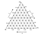
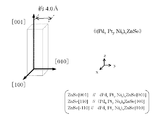
【解決手段】正孔注入電極15であって、組成式(PdxPtyNiz)uZnSe(ただし、uは4≦u≦6の実数であり、x、y、zはx+y+z=1、1>x≧0、1>y≧0、1>z≧0の実数)で示される材料からなる電極層を有する。半導体素子であって、組成式(Zn1−α−βMgαCdβ)(Se1−m−nSmTen)(ただし、モル比m、nおよびα、βは、m+n≦1、0≦m≦1、0≦n≦0.2、0≦α≦0.2、0≦β≦0.2)で示される材料からなるP型半導体層14と、電極層がP型半導体層14と接するように形成された正孔注入電極15と、を有してもよい。
【選択図】図1
Description
などの手法が採用されている。

蒸着は、基板温度を200℃に保持し、Zn、Se、Cu各原料の加熱設定温度をそれぞれ250℃、150℃、1000℃として行った。このときの各原料の分圧比はZn:Se:Cu≒25:80:1であった。
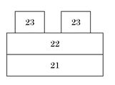
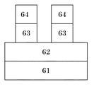
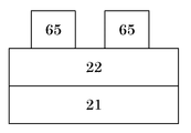
12 n型用電極
13 n型半導体
14 p型半導体
15 正孔注入電極(電極層を含む)
Claims (9)
- 組成式(PdxPtyNiz)uZnSe(ただし、uは4≦u≦6の実数であり、x、y、zはx+y+z=1、1>x≧0、1>y≧0、1>z≧0の実数)で示される材料からなる電極層を有することを特徴とする正孔注入電極。
- 組成式(Zn1−α−βMgαCdβ)(Se1−m−nSmTen)(ただし、モル比m、nおよびα、βは、m+n≦1、0≦m≦1、0≦n≦0.2、0≦α≦0.2、0≦β≦0.2)で示される材料からなる半導体層と、
請求項1に記載の正孔注入電極であって前記電極層が前記半導体層と接するように形成された正孔注入電極と、
を有することを特徴とする半導体素子。 - 前記半導体層が[001]軸配向した単結晶からなり、かつ、前記電極層の[001]軸が前記半導体層の[001]軸と略平行であることを特徴とする請求項2に記載の半導体素子。
- 前記半導体層が[001]軸優先配向した多結晶体からなり、かつ、前記電極層の[001]軸が前記半導体層の[001]軸と略平行であることを特徴とする請求項2に記載の半導体素子。
- 前記半導体層及び前記電極層は、ガラス基板上に形成されていることを特徴とする請求項4に記載の半導体素子。
- 前記電極層の厚みが、10nm以上10μm以下であることを特徴とする請求項2乃至5のいずれかに記載の半導体素子。
- 前記半導体層が、1×1018cm−3以上1×1022cm−3以下の正孔濃度を有する
ことを特徴とする請求項2乃至6のいずれかに記載の半導体素子。 - 前記半導体層が、Cuドーパントを含むp型半導体層であることを特徴とする請求項2乃至7のいずれかに記載の半導体素子。
- 前記半導体素子が発光ダイオード、ダイオード、レーザダイオード、フォトダイオード、もしくは、太陽電池であることを特徴とする請求項2乃至8のいずれかに記載の半導体素子。
Priority Applications (1)
| Application Number | Priority Date | Filing Date | Title |
|---|---|---|---|
| JP2004105125A JP4401843B2 (ja) | 2004-03-31 | 2004-03-31 | 正孔注入電極及び半導体素子 |
Applications Claiming Priority (1)
| Application Number | Priority Date | Filing Date | Title |
|---|---|---|---|
| JP2004105125A JP4401843B2 (ja) | 2004-03-31 | 2004-03-31 | 正孔注入電極及び半導体素子 |
Publications (2)
| Publication Number | Publication Date |
|---|---|
| JP2005294415A true JP2005294415A (ja) | 2005-10-20 |
| JP4401843B2 JP4401843B2 (ja) | 2010-01-20 |
Family
ID=35327034
Family Applications (1)
| Application Number | Title | Priority Date | Filing Date |
|---|---|---|---|
| JP2004105125A Expired - Fee Related JP4401843B2 (ja) | 2004-03-31 | 2004-03-31 | 正孔注入電極及び半導体素子 |
Country Status (1)
| Country | Link |
|---|---|
| JP (1) | JP4401843B2 (ja) |
Cited By (6)
| Publication number | Priority date | Publication date | Assignee | Title |
|---|---|---|---|---|
| JP2008013414A (ja) * | 2006-07-07 | 2008-01-24 | Sumitomo Electric Ind Ltd | セレン化亜鉛多結晶およびその製造方法 |
| JP2008166343A (ja) * | 2006-12-27 | 2008-07-17 | Matsushita Electric Ind Co Ltd | 線状発光装置 |
| JP2008255444A (ja) * | 2007-04-06 | 2008-10-23 | Hoya Corp | ZnCuSe薄膜付き基板およびその製造方法 |
| JP2009064886A (ja) * | 2007-09-05 | 2009-03-26 | Toshiba Corp | 半導体レーザ装置 |
| US7737458B2 (en) | 2008-02-25 | 2010-06-15 | Panasonic Corporation | Light emitting device having a straight-line shape |
| US8330177B2 (en) | 2007-02-27 | 2012-12-11 | Panasonic Corporation | Display device |
-
2004
- 2004-03-31 JP JP2004105125A patent/JP4401843B2/ja not_active Expired - Fee Related
Cited By (6)
| Publication number | Priority date | Publication date | Assignee | Title |
|---|---|---|---|---|
| JP2008013414A (ja) * | 2006-07-07 | 2008-01-24 | Sumitomo Electric Ind Ltd | セレン化亜鉛多結晶およびその製造方法 |
| JP2008166343A (ja) * | 2006-12-27 | 2008-07-17 | Matsushita Electric Ind Co Ltd | 線状発光装置 |
| US8330177B2 (en) | 2007-02-27 | 2012-12-11 | Panasonic Corporation | Display device |
| JP2008255444A (ja) * | 2007-04-06 | 2008-10-23 | Hoya Corp | ZnCuSe薄膜付き基板およびその製造方法 |
| JP2009064886A (ja) * | 2007-09-05 | 2009-03-26 | Toshiba Corp | 半導体レーザ装置 |
| US7737458B2 (en) | 2008-02-25 | 2010-06-15 | Panasonic Corporation | Light emitting device having a straight-line shape |
Also Published As
| Publication number | Publication date |
|---|---|
| JP4401843B2 (ja) | 2010-01-20 |
Similar Documents
| Publication | Publication Date | Title |
|---|---|---|
| CN100405618C (zh) | 发光元件及其制造方法 | |
| JP4787496B2 (ja) | ハイブリッドビーム堆積システム及び方法並びにそれによって作製された半導体デバイス | |
| KR100582250B1 (ko) | N형 산화아연층과 p형 반도체 층을 가지는 발광 다이오드 및 레이저 다이오드 | |
| US6791257B1 (en) | Photoelectric conversion functional element and production method thereof | |
| JP4270885B2 (ja) | 酸化物半導体発光素子 | |
| CN100485977C (zh) | 发光二极管 | |
| JPH0268968A (ja) | 化合物半導体発光素子 | |
| KR101030823B1 (ko) | 투명 박막, 이를 포함하는 발광 소자와 이들의 제조 방법 | |
| JP4401843B2 (ja) | 正孔注入電極及び半導体素子 | |
| JP4285837B2 (ja) | 窓層を備えたAlGaInP発光素子 | |
| JP4233570B2 (ja) | 半導体材料およびこれを用いた半導体素子 | |
| JP2003060235A (ja) | Ii−vi族化合物半導体結晶および光電変換機能素子 | |
| KR100827993B1 (ko) | 질화갈륨계 반도체 소자 | |
| US8294146B2 (en) | ZnO-containing semiconductor layer and device using the same | |
| JP2004349584A (ja) | 酸化物半導体発光素子 | |
| JPH09219539A (ja) | 窒化物半導体素子及びその製造方法 | |
| JP4705384B2 (ja) | 窒化ガリウム系半導体素子 | |
| JP4278394B2 (ja) | 酸化物半導体発光素子 | |
| JP2003110142A (ja) | 酸化物半導体発光素子およびその製造方法 | |
| JP5115277B2 (ja) | 発光素子 | |
| KR100389738B1 (ko) | 단파장 산화아연 발광소자 및 그 제조방법 | |
| Liu et al. | Light-Emitting Diodes Based on p-GaN/i-ZnO/n-ZnO Heterojunctions | |
| JPH09162443A (ja) | 半導体発光素子 | |
| JPH04188880A (ja) | 化合物半導体発光素子 | |
| JP2002173399A (ja) | ZnTe基板および光電変換機能素子 |
Legal Events
| Date | Code | Title | Description |
|---|---|---|---|
| A621 | Written request for application examination |
Free format text: JAPANESE INTERMEDIATE CODE: A621 Effective date: 20060728 |
|
| A977 | Report on retrieval |
Free format text: JAPANESE INTERMEDIATE CODE: A971007 Effective date: 20090603 |
|
| A131 | Notification of reasons for refusal |
Free format text: JAPANESE INTERMEDIATE CODE: A131 Effective date: 20090616 |
|
| A521 | Request for written amendment filed |
Free format text: JAPANESE INTERMEDIATE CODE: A523 Effective date: 20090814 |
|
| TRDD | Decision of grant or rejection written | ||
| A01 | Written decision to grant a patent or to grant a registration (utility model) |
Free format text: JAPANESE INTERMEDIATE CODE: A01 Effective date: 20091027 |
|
| A01 | Written decision to grant a patent or to grant a registration (utility model) |
Free format text: JAPANESE INTERMEDIATE CODE: A01 |
|
| A61 | First payment of annual fees (during grant procedure) |
Free format text: JAPANESE INTERMEDIATE CODE: A61 Effective date: 20091028 |
|
| R150 | Certificate of patent or registration of utility model |
Free format text: JAPANESE INTERMEDIATE CODE: R150 |
|
| FPAY | Renewal fee payment (event date is renewal date of database) |
Free format text: PAYMENT UNTIL: 20121106 Year of fee payment: 3 |
|
| FPAY | Renewal fee payment (event date is renewal date of database) |
Free format text: PAYMENT UNTIL: 20121106 Year of fee payment: 3 |
|
| FPAY | Renewal fee payment (event date is renewal date of database) |
Free format text: PAYMENT UNTIL: 20131106 Year of fee payment: 4 |
|
| R250 | Receipt of annual fees |
Free format text: JAPANESE INTERMEDIATE CODE: R250 |
|
| LAPS | Cancellation because of no payment of annual fees |