JP2005290550A - Sputtering equipment - Google Patents
Sputtering equipment Download PDFInfo
- Publication number
- JP2005290550A JP2005290550A JP2005040668A JP2005040668A JP2005290550A JP 2005290550 A JP2005290550 A JP 2005290550A JP 2005040668 A JP2005040668 A JP 2005040668A JP 2005040668 A JP2005040668 A JP 2005040668A JP 2005290550 A JP2005290550 A JP 2005290550A
- Authority
- JP
- Japan
- Prior art keywords
- targets
- magnetic field
- film
- field forming
- target
- Prior art date
- Legal status (The legal status is an assumption and is not a legal conclusion. Google has not performed a legal analysis and makes no representation as to the accuracy of the status listed.)
- Granted
Links
Images
Classifications
-
- C—CHEMISTRY; METALLURGY
- C23—COATING METALLIC MATERIAL; COATING MATERIAL WITH METALLIC MATERIAL; CHEMICAL SURFACE TREATMENT; DIFFUSION TREATMENT OF METALLIC MATERIAL; COATING BY VACUUM EVAPORATION, BY SPUTTERING, BY ION IMPLANTATION OR BY CHEMICAL VAPOUR DEPOSITION, IN GENERAL; INHIBITING CORROSION OF METALLIC MATERIAL OR INCRUSTATION IN GENERAL
- C23C—COATING METALLIC MATERIAL; COATING MATERIAL WITH METALLIC MATERIAL; SURFACE TREATMENT OF METALLIC MATERIAL BY DIFFUSION INTO THE SURFACE, BY CHEMICAL CONVERSION OR SUBSTITUTION; COATING BY VACUUM EVAPORATION, BY SPUTTERING, BY ION IMPLANTATION OR BY CHEMICAL VAPOUR DEPOSITION, IN GENERAL
- C23C14/00—Coating by vacuum evaporation, by sputtering or by ion implantation of the coating forming material
- C23C14/22—Coating by vacuum evaporation, by sputtering or by ion implantation of the coating forming material characterised by the process of coating
- C23C14/34—Sputtering
- C23C14/35—Sputtering by application of a magnetic field, e.g. magnetron sputtering
-
- C—CHEMISTRY; METALLURGY
- C23—COATING METALLIC MATERIAL; COATING MATERIAL WITH METALLIC MATERIAL; CHEMICAL SURFACE TREATMENT; DIFFUSION TREATMENT OF METALLIC MATERIAL; COATING BY VACUUM EVAPORATION, BY SPUTTERING, BY ION IMPLANTATION OR BY CHEMICAL VAPOUR DEPOSITION, IN GENERAL; INHIBITING CORROSION OF METALLIC MATERIAL OR INCRUSTATION IN GENERAL
- C23C—COATING METALLIC MATERIAL; COATING MATERIAL WITH METALLIC MATERIAL; SURFACE TREATMENT OF METALLIC MATERIAL BY DIFFUSION INTO THE SURFACE, BY CHEMICAL CONVERSION OR SUBSTITUTION; COATING BY VACUUM EVAPORATION, BY SPUTTERING, BY ION IMPLANTATION OR BY CHEMICAL VAPOUR DEPOSITION, IN GENERAL
- C23C14/00—Coating by vacuum evaporation, by sputtering or by ion implantation of the coating forming material
- C23C14/22—Coating by vacuum evaporation, by sputtering or by ion implantation of the coating forming material characterised by the process of coating
- C23C14/34—Sputtering
- C23C14/3464—Sputtering using more than one target
Landscapes
- Chemical & Material Sciences (AREA)
- Chemical Kinetics & Catalysis (AREA)
- Engineering & Computer Science (AREA)
- Materials Engineering (AREA)
- Mechanical Engineering (AREA)
- Metallurgy (AREA)
- Organic Chemistry (AREA)
- Physical Vapour Deposition (AREA)
Abstract
【課題】異常放電や非エロージョン部を低減し、膜厚分布が均一な膜を成膜可能な成膜装置を提供する。
【解決手段】本発明の成膜装置1は複数のターゲット31a〜31fを有しており、異なるターゲット31a〜31fに同じ異なる極性の交流電圧が印加される。一方のターゲット31a〜31fが負電位に置かれる時には他方のターゲット31a〜31fが正電位に置かれ、アノード電極として作用するので、隣合うターゲット31a〜31fの間にアノード電極を配置する必要がない。隣合うターゲット31a〜31fの間には何も配置されていないので、ターゲット31a〜31f間の距離sを短くすることが可能であり、ターゲット31a〜31fが配置された領域のうち、スパッタ粒子が放出されない面積の割合が少なくなるので、スパッタ粒子が基板5に均一に到達し、膜厚分布が均一になる。
【選択図】図1
Disclosed is a film forming apparatus capable of reducing an abnormal discharge and a non-erosion portion and forming a film having a uniform film thickness distribution.
A film forming apparatus 1 of the present invention has a plurality of targets 31a to 31f, and AC voltages having the same polarity are applied to different targets 31a to 31f. When one target 31a to 31f is placed at a negative potential, the other target 31a to 31f is placed at a positive potential and acts as an anode electrode, so that it is not necessary to place an anode electrode between adjacent targets 31a to 31f. . Since nothing is arranged between the adjacent targets 31a to 31f, the distance s between the targets 31a to 31f can be shortened, and sputtered particles are in the region where the targets 31a to 31f are arranged. Since the proportion of the area that is not released decreases, the sputtered particles uniformly reach the substrate 5 and the film thickness distribution becomes uniform.
[Selection] Figure 1
Description
本発明はスパッタリング装置に関する。 The present invention relates to a sputtering apparatus.
図8の符号101は従来技術の成膜装置を示している。
成膜装置101は真空槽102と、真空槽102内部に配置された複数のターゲット131a〜131eとを有している。
The
各ターゲット131a〜131eは細長の板状であって、真空槽102内部に配置された基板105にスパッタ面が向けられた状態で一定以上の間隔を空けて互いに平行に配置されている。
Each of the
真空排気系112により真空槽102内部を真空排気しながら、ガス供給系113から真空槽102内部にスパッタガスを導入し、真空槽102内部に成膜雰囲気を形成した状態で、電極135a〜135eが接続された電源117a〜117eを起動し、真空槽102と基板104を接地電位に置いた状態で各ターゲット131a〜131eに交流電圧を印加すると、ターゲット131a〜131eの表面がスパッタされる。
While evacuating the inside of the
複数のターゲット131a〜131eを同時にスパッタする場合、接地電位に置かれたシールド111がターゲット131a〜131eの周辺部だけに配置されていると、シールド111が配置された方向にプラズマが偏ってしまうが、この成膜装置101ではターゲット131a〜131eの間にも接地電位に置かれたシールド111が配置されているため、プラズマが偏らず、各ターゲット131a〜131eが均一にスパッタされる。
When sputtering a plurality of
ターゲット131a〜131eのスパッタ面とは反対側には細長の磁界形成手段140a〜140eがターゲット131a〜131eの長手方向に沿って配置されている。磁界形成手段140a〜140eの幅はターゲット131a〜131eの幅よりも短く、不図示の移動手段によってターゲット131a〜131eの幅方向の一端から他端まで往復移動するようになっている。
On the opposite side of the
従って磁界形成手段140a〜140eによって形成される磁界もターゲット131a〜131e表面を移動するので、プラズマ密度の高い部分がターゲット131a〜131e表面を移動し、ターゲット131a〜131eの広い領域がスパッタされることになる。
Therefore, since the magnetic field formed by the magnetic field forming means 140a to 140e also moves on the surfaces of the
複数のターゲットを用いた成膜装置では、ターゲットの数が多い分、広い領域にスパッタ粒子が放出されるため、大面積の基板105に成膜を行うことが可能である。
In a film formation apparatus using a plurality of targets, sputtered particles are emitted in a wide area as the number of targets increases, so that a film can be formed on the
しかしながら、従来の成膜装置には以下に述べる問題点があった。先ず、第一に、シールド111が位置する部分からはスパッタ粒子が放出されないため、基板105の表面のシールド111上に位置する部分と、ターゲット131a〜131e上に位置する部分で膜厚分布及び膜質分布に不均一が生じる。
However, the conventional film forming apparatus has the following problems. First, since the sputtered particles are not emitted from the portion where the
また、上述したように磁界形成手段140a〜140eを移動させながら、ターゲット131a〜131eに交流電圧を印加する場合には、磁界形成手段140a〜140eの移動に伴い、プラズマ密度の高い部分も移動してしまう。
In addition, when an AC voltage is applied to the
従って、スパッタガスと一緒に酸素ガスのような反応性ガスを導入してスパッタリングを行う場合には、プラズマ密度が高い部分が移動してしまうと、スパッタ面のプラズマ密度が薄くなった部分でターゲット材料と反応性ガスが反応して反応物の膜(例えば酸化膜)が形成されてしまい、異常放電の原因となる。 Therefore, when sputtering is performed by introducing a reactive gas such as oxygen gas together with the sputtering gas, if the portion with a high plasma density moves, the target becomes a portion with a reduced plasma density on the sputtering surface. The material and the reactive gas react to form a reactant film (for example, an oxide film), which causes abnormal discharge.
磁界形成手段140a〜140eを移動させずに固定してスパッタリングを行えば、プラズマ密度の高い部分の移動は起こらないが、ターゲット131a〜131e内(特にターゲット131a〜131eの幅方向の中央部分)に非エロージョン部が生じ、この非エロージョン部が異常放電の原因となったり、また非エロージョン部が剥離してパーティクルが発生する原因ともなる。
If sputtering is performed without moving the magnetic field forming means 140a to 140e without moving, the portion with a high plasma density does not move, but within the
本発明は上記従来技術の不都合を解決するために創作されたものであり、その目的は、エロージョン領域が広く、異常放電がなく、膜厚分布が均一な薄膜を形成できる成膜装置を提供するものである。 The present invention was created to solve the above-described disadvantages of the prior art, and an object thereof is to provide a film forming apparatus capable of forming a thin film having a wide erosion region, no abnormal discharge, and a uniform film thickness distribution. Is.
上記課題を解決するために請求項1記載の発明は、真空槽と、複数の長手方向を有する板状のターゲットと、前記ターゲットに交流電圧を印加する交流電源とを有し、前記複数のターゲットのうち、異なるターゲットに同じ交流電源から極性が異なる交流電圧が印加され、前記複数のターゲットはスパッタ面が同じ方向に向けられた状態で、隣合う前記ターゲットの長手方向の側面が、前記真空槽中の雰囲気のみを介して互いに直接対向するように配置された成膜装置である。
請求項2記載の発明は、請求項1記載の成膜装置であって、互いに対向する前記側面同士の距離は1mm以上10mm以下にされた成膜装置である。
請求項3記載の発明は、請求項1又は請求項2のいずれか1項記載の成膜装置であって、前記交流電源部の周波数は1kHz以上100kHz以下であることを特徴とする成膜装置である。
請求項4記載の発明は、真空槽と、前記真空槽の内部に配置された複数の細長の板状ターゲットとを有し、前記各ターゲットは長手方向の側面同士が対向するように互いに平行に配置され、前記各ターゲットの真裏位置には、細長の磁界形成手段が前記ターゲットの長手方向に沿ってそれぞれ配置され、前記磁界形成手段が配置された領域の外側であって、前記ターゲットの真裏位置よりも外側には、細長の補助磁界形成手段が前記ターゲットの長手方向に沿って配置された成膜装置である。
請求項5記載の発明は、請求項4記載の成膜装置であって、前記各磁界形成手段は複数の磁石を有し、前記複数の磁石のうち、前記補助磁界形成手段に隣接して配置された磁石の前記ターゲット側に向けられた面の磁極は、前記補助磁界形成手段の前記ターゲット側に向けられた面の磁極と同じ極性にされた成膜装置である。
請求項6記載の発明は、請求項4又は請求項5のいずれか1項記載の成膜装置であって、前記磁界形成手段と前記補助磁界形成手段を、前記ターゲットに対して相対的に移動させる移動手段を有する成膜装置である。
In order to solve the above-mentioned problem, the invention described in
A second aspect of the present invention is the film forming apparatus according to the first aspect, wherein the distance between the side surfaces facing each other is 1 mm or more and 10 mm or less.
A third aspect of the present invention is the film forming apparatus according to any one of the first or second aspects, wherein the frequency of the AC power supply unit is 1 kHz or more and 100 kHz or less. It is.
The invention described in claim 4 has a vacuum chamber and a plurality of elongated plate-like targets arranged inside the vacuum chamber, and the targets are parallel to each other so that the side surfaces in the longitudinal direction face each other. The elongated magnetic field forming means is disposed along the longitudinal direction of the target at the position directly behind each of the targets, and is located outside the area where the magnetic field forming means is disposed, On the outer side, a thin auxiliary magnetic field forming means is disposed along the longitudinal direction of the target.
A fifth aspect of the present invention is the film forming apparatus according to the fourth aspect, wherein each of the magnetic field forming means has a plurality of magnets, and is arranged adjacent to the auxiliary magnetic field forming means among the plurality of magnets. In the film forming apparatus, the magnetic pole of the surface directed toward the target of the magnet formed has the same polarity as the magnetic pole of the surface directed toward the target of the auxiliary magnetic field forming unit.
The invention according to claim 6 is the film forming apparatus according to
本発明は上記のように構成されており、隣接するターゲット同士の間にアース電極も絶縁物も配置されておらず、従って真空槽内部を真空排気したときに、隣合うターゲットの長手方向の側面が対向する領域にも真空雰囲気が形成され、該真空雰囲気の幅は、側面同士の距離と等しくなる。 The present invention is configured as described above, and neither an earth electrode nor an insulator is disposed between adjacent targets. Therefore, when the inside of the vacuum chamber is evacuated, the side surface in the longitudinal direction of the adjacent target A vacuum atmosphere is also formed in the regions facing each other, and the width of the vacuum atmosphere is equal to the distance between the side surfaces.
何も配置されていない分、側面同士の距離を1mm以上10mm以下と小さくすることが可能であるので、スパッタ粒子が放出されない領域が狭くなり、従って基板に到達するスパッタ粒子の量の分布が均一になる。 Since nothing is arranged, the distance between the side surfaces can be made as small as 1 mm or more and 10 mm or less, so the area where the sputtered particles are not released becomes narrow, and the distribution of the amount of sputtered particles reaching the substrate is uniform. become.
磁界形成手段の幅をターゲットの幅と略等しくすれば、磁界形成手段を移動させずにスパッタを行っても、ターゲットの表面全域のプラズマ密度を高くすることができるが、上述したようにターゲット同士の間隔が短い場合には、磁界形成手段同士の間隔も短くなってしまう。磁界形成手段を複数台近接させて配置した場合、隣接しあう磁界形成手段同士の磁場干渉で磁場バランスが崩れてしまう。特に、交流電源を用いてスパッタを行う場合は対になるカソード(ターゲット)同士の放電インピーダンスが異なるために、膜厚、膜質分布の劣化、さらには対になるカソード同士のターゲット使用効率の劣化が問題となる。 If the width of the magnetic field forming means is substantially equal to the width of the target, the plasma density over the entire surface of the target can be increased even if sputtering is performed without moving the magnetic field forming means. When the distance between the magnetic field forming means is short, the distance between the magnetic field forming means is also shortened. When a plurality of magnetic field forming means are arranged close to each other, the magnetic field balance is lost due to magnetic field interference between adjacent magnetic field forming means. In particular, when sputtering is performed using an AC power source, the discharge impedances of the paired cathodes (targets) are different, resulting in deterioration of film thickness and film quality distribution, and further deterioration of target use efficiency between the paired cathodes. It becomes a problem.
本発明の成膜装置では、ターゲットが配置された領域よりも外側であって、最も外側に配置された磁界形成手段の近傍位置に補助磁界形成手段を有しており、この補助磁界形成手段によって、磁界形成手段を近接させた場合の磁場干渉が緩和されるので、磁場強度のバランスが崩れず、各ターゲットの表面で磁束密度の分布が均一になる。 In the film forming apparatus of the present invention, the auxiliary magnetic field forming means is provided outside the area where the target is arranged and in the vicinity of the magnetic field forming means arranged on the outermost side. Since the magnetic field interference when the magnetic field forming means is brought close is relaxed, the balance of the magnetic field strength is not lost, and the distribution of the magnetic flux density becomes uniform on the surface of each target.
磁界形成手段をターゲットに対して相対的に移動させながら、スパッタリングを行う場合には、磁力線が遠ざかり、プラズマ密度が少なくなった部分はスパッタされず、ターゲットの表面に反応性ガスとの反応物(例えば酸化物)が形成されてしまい、その反応物が異常放電やパーティクルの原因になるが、上述したように本発明では磁界形成手段を移動させる必要がなく、ターゲットに対して固定した状態でスパッタリングを行えるので、異常放電が起こらない。 When sputtering is performed while moving the magnetic field forming unit relative to the target, the portion where the magnetic lines of force move away and the plasma density is reduced is not sputtered, and a reaction product with a reactive gas ( For example, an oxide) is formed, and the reaction product causes abnormal discharge and particles. However, as described above, in the present invention, it is not necessary to move the magnetic field forming means, and sputtering is performed while being fixed to the target. Therefore, abnormal discharge does not occur.
本発明の成膜装置を用いれば、大型基板に成膜した場合であっても、膜厚分布、および膜質分布が良い膜が得られることができる。また、アースシールド部品が不要となったため、アースシールド部品部分からのパーティクルが低減された。さらに、従来装置と比べ、アースシールド部品、磁気回路の揺動機構、電源の異常放電防止機構が必要なくなったため、部品点数が削減でき、コスト削減、装置メンテナンス性の改善ができた。 By using the film forming apparatus of the present invention, a film having a good film thickness distribution and film quality distribution can be obtained even when the film is formed on a large substrate. In addition, since the earth shield part is not required, particles from the earth shield part are reduced. Furthermore, as compared with the conventional device, the earth shield component, the magnetic circuit swinging mechanism, and the power supply abnormal discharge prevention mechanism are no longer required, so the number of components can be reduced, the cost can be reduced, and the device maintainability can be improved.
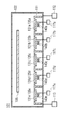
図1の符号1は本発明の成膜装置の一例を示しており、この成膜装置1は真空槽2と、真空槽2内部に配置された基板ホルダ4と、真空槽2内部の基板ホルダ4と対向する位置に配置されたスパッタ源3とを有している。スパッタ源3は複数のスパッタ部30a〜30fを有している。各スパッタ部30a〜30fは板状のターゲット31a〜31fをそれぞれ有しており、各ターゲット31a〜31fのスパッタされる面をスパッタ面とすると、各スパッタ部30a〜30fは各スパッタ面が同じ平面上に位置するように配置されている。
各ターゲット31a〜31fは長手方向を有する細長に成形されており、各スパッタ面も長手方向を有する細長になっている。各ターゲット31a〜31fはそれぞれ同一形状であり、スパッタ面の長手方向の縁部分(側面)が互いに所定間隔を空けて平行に配置されている。
Each of the
隣り合うターゲット31a〜31fの側面同士は一定距離だけ離間するように形成されており、従って、隣接するターゲット31a〜31fの側面は平行になる。本発明ではターゲット31a〜31f間には電極もシールドも配置されておらず、ターゲット31a〜31fの側面同士は直接面するようになっている。
The side surfaces of the
各ターゲット31a〜31fの裏面には、ターゲット31a〜31fと同じ幅、同じ長さの電極35a〜35fが、ターゲット31a〜31fの外周からはみ出さないように密着して取り付けられている。
真空槽2の外部には交流電源17a〜17cが配置されており、各交流電源17a〜17cの2つの端子のうち、一方の端子は隣接する2つの電極35a〜35fのうち一方の電極35a、35c、35eに接続され、他方の端子は他方の電極35b、35d、35fに接続されている。
各交流電源17a〜17cの2つの端子は正負の異なる極性の電圧を出力するようになっており、ターゲット31a〜31fは電極35a〜35fに密着して取り付けられているので、隣接する2つのターゲット31a〜31fには互いに異なる極性の交流電圧が交流電源17a〜17cから印加される。従って、互いに隣接するターゲット31a〜31fのうち、一方が正電位に置かれる時には他方が負電位に置かれた状態になる。
Two terminals of each of the
電極35a〜35fのターゲット31a〜31fとは反対側の面には絶縁板33a〜33fが取り付けられており、ターゲット31a〜31f及び電極35a〜35fは、後述する磁界形成手段40a〜40fや他の部材から絶縁されるようになっている。
Insulating
電極35a〜35fのターゲット31a〜31fとは反対側の面には磁界形成手段40a〜40fが配置されている。図2を参照し、各磁界形成手段40a〜40fは、外周がターゲット31a〜31fの外周と略等しい大きさの細長のリング状磁石42a〜42fと、リング状磁石42a〜42fの長さよりも短い棒状磁石43a〜43fとそれぞれ有している。
Magnetic field forming means 40a to 40f are arranged on the surfaces of the
各リング状磁石42a〜42fは、対応する1個のターゲット31a〜31fの真裏位置で、ターゲット31a〜31fの長手方向に対して平行に配置されている。上述したように、ターゲット31a〜31fは所定間隔を空けて平行配置されているので、リング状磁石42a〜42fはターゲット31a〜31fと同じ間隔を空けて配置された状態になっている。
Each of the ring-shaped
棒状磁石43a〜43fは、リング状磁石42a〜42fのリングの内部にターゲット31a〜31fの長手方向に沿って配置されている。従って、棒状磁石43a〜43fの長手方向の側面の両側には、リング状磁石42a〜42fが配置された状態になっている。
The rod-shaped
磁界形成手段40a〜40fの磁石のうち、両側に配置され磁石(リング状磁石)を第一の磁石42a〜42fとし、第一の磁石42a〜42fの間に配置された磁石(棒状磁石)を第二の磁石43a〜43fとすると、第一、第二の磁石42a〜42f、43a〜43fの磁極は、厚み方向の両端、即ち表面側と裏面側に位置しており、ターゲット31a〜31f側に向けられた面を表面とすると、第一、第二の磁石42a〜42f、43a〜43fの裏面側には板状のヨーク41a〜41fが密着されている。
Among the magnets of the magnetic field forming means 40a to 40f, the magnets (ring magnets) arranged on both sides are
従って、第一、第二の磁石42a〜42f、43a〜43fの裏面側の磁極の間に発生する磁力線は、ヨーク41a〜41fの内部を通るようになっている。ヨーク41a〜41fの平面形状は第一の磁石42a〜42fのリングの外周と等しく、第一の磁石42a〜42fはヨーク41a〜41fの縁からはみ出さないように配置されている。上述したように第一の磁石42a〜42fの形状はターゲット31a〜31fと略等しいので、磁界形成手段40a〜40fの平面形状もターゲット31a〜31fと略等しくなる。
ここでは、各磁界形成手段40a〜40fは対応する1つのターゲット31a〜31fの真裏位置で配置されているので、各磁界形成手段40a〜40fはターゲット13a〜31fの外周からはみ出さず、各磁界形成手段40a〜41fが2つのターゲット31a〜31fに渡って配置されてはいない。
Therefore, the lines of magnetic force generated between the magnetic poles on the back side of the first and
Here, since each magnetic field formation means 40a-40f is arrange | positioned in the back position of one
第一の磁石42a〜42fは表面側の磁極の磁性がN極の場合は、第二の磁石43a〜43fの表面側の磁極の磁性はS極、第一の磁石42a〜42fの表面側の磁極の磁性がS極の場合は、第二の磁石43a〜43fの表面側の磁極の磁性はN極になっており、従って、第一の磁石42a〜42fの表面と、第二の磁石43a〜43fの表面の間には、電極35a〜35fを通る磁力線が形成される。
When the
各電極35a〜35fの内部の、第一、第二の磁石42a〜42f上の位置には、透磁性材料(ここでは純度99.8%の純鉄)からなる磁性体36a〜36fがそれぞれ配置されており、電極35a〜35fを通る磁力線はこの磁性体36a〜36fによってターゲット31a〜31f側に引き付けられ、ターゲット31a〜31fの表面を通るようになっている。
各スパッタ部30a〜30fの第一の磁石42a〜42fの同じ極性の磁極は、同じ面側に位置しており、従って第一の磁石42a〜42fのターゲット31a〜31f側の極性は全てがN極、又はS極のいずれかになっている。
The magnetic poles of the same polarity of the
上述したように、第二の磁石43a〜43fは第一の磁石42a〜42aと同じ面側の磁極の極性は、第一の磁石42a〜42fとは反対になっているので、第一の磁石42a〜42fのターゲット31a〜31f側の極性が全てN極の場合は、第二の磁石43a〜43fのターゲット31a〜31f側の極性は全てがS極になっており、第一の磁石42a〜42fのターゲット31a〜31f側の極性が全てS極の場合は、第二の磁石43a〜43fのターゲット31a〜31f側の極性は全てN極になっている。
As described above, the
従って、同じスパッタ部30a〜30fの第一、第二の磁石42a〜42f、43a〜43fの間には磁力線が形成されるが、異なるスパッタ部30a〜30fの隣接する第一の磁石42a〜42f間には磁力線が形成されないようになっている。
Therefore, although magnetic lines of force are formed between the first and
スパッタ源3は補助磁界形成手段15a、15bを有している。補助磁界形成手段15a、15bは第一の磁石42a〜42fの長さと略等しい長さの細長の棒状磁石で構成されており、第一の磁石42a〜42fの並べられた領域の外側に、第一の磁石42a〜42fの長手方向に沿って配置されている。
The
補助磁界形成手段15a、15bは、第一、第二の磁石42a〜42f、43a〜43fと同じ高さに位置している。図1の符号42aと符号42fは、第1の磁石42a〜42fのうち、列の先頭と終わりに位置する第一の磁石を示している。列の先頭と終わりに位置する第一の磁石42a、42fの2つの長手方向の側面のうち、列の中心方向を向く側面ではなく、外方向に面する側面を端部面とすると、その端部面は補助磁界形成手段15a、15bの長手方向の側面と密着又は離間している。
The auxiliary magnetic field forming means 15a and 15b are located at the same height as the first and
図3は第一、第二の磁石42a〜42f、43a〜43fと補助磁界形成手段15a、15bとの磁極の関係の一例を示す図である。補助磁界形成手段15a、15bの磁極は厚み方向の両端、即ち表面側と裏面側に位置し、第一、第二の磁石42a〜42f、43a〜43fの表面と同じ側に向けられた面を表面とすると、補助磁界形成手段15a、15bの裏面はヨーク16a、16に密着しており、従って補助磁界形成手段15a、15bの裏面側の磁極から発生する磁力線はヨーク16a、16bの内部を通るようになっている。
FIG. 3 is a diagram showing an example of the relationship between the magnetic poles of the first and
補助磁界形成手段15a、15bの表面側の磁極の磁性は、第一の磁石42a〜42fの表面側の磁極の磁性と同じになっている。従って、第一の磁石42a〜42fの表面側の磁極の磁性がN極の場合には、補助磁界形成手段15a、15bの表面側の磁極の磁性はN極であり、第一の磁石42a〜42fの表面側の磁極の磁性がS極の場合は、補助磁界形成手段15a、15bの表面側の磁極の磁性はS極になる。
The magnetic properties of the magnetic poles on the surface side of the auxiliary magnetic
上述したように、補助磁界形成手段15a、15bは最も外側に位置する第一の磁石42a、42fに沿って配置されているので、補助磁界形成手段15a、15bと、最も外側に位置する第一の磁石42a、42fとが1つの磁石として機能し、その磁石の表面と、隣接する第二の磁石43a、43f表面との間で、最も外側に位置するターゲット31a、31fを通る磁力線が発生する。
As described above, the auxiliary magnetic field forming means 15a and 15b are arranged along the outermost
ここでは、列の先頭と終わりに位置するターゲット31a、31fの、2つの長手方向の側面のうち、列の中心方向を向く側面でなく、外方向に面する側面の真下には、第1の磁石42a、42fの端部面が位置している。
従って、補助磁界形成手段15a、15bは、最も外側に位置するターゲット31a、31fの真裏位置よりも外側に配置されており、最も外側に位置するターゲット31a、31fの表面を通る磁力線の磁束強度は、そのターゲット31a、31fの端部位置でも弱くならない。
Here, of the two longitudinal side surfaces of the
Accordingly, the auxiliary magnetic field forming means 15a and 15b are disposed outside the position directly behind the
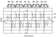
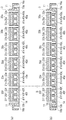
図6はスパッタ部30a〜30eを5個並べて配置し、最も外側に位置する第一の磁石15a、15eに近接して補助磁界形成手段15a、15bを配置した場合の、ターゲット31a〜31e表面の磁束密度を測定した結果を、磁界形成手段40a〜40e及び補助磁界形成手段15a、15bの位置と一緒に表した図である。尚、図6と後述する図7の符号Bvはターゲット31a〜31eの表面に対して垂直方向の磁束密度を、符号Bhはターゲット31a〜31eの表面に対して平行方向の磁束密度を、横軸は5個のターゲット31a〜31eの列の中央位置をゼロとした場合の中央からの距離を、縦軸は磁束密度(G:ガウス)をそれぞれ示している。
FIG. 6 shows the surfaces of the
図6示すように、磁束密度は平行方向の分布は台型で、かつ垂直方向の分布は0を交差する点が2点以上(ここでは3点)存在するような形状を示している。このような磁場形状の磁力線が形成されることにより、磁石を揺動しなくても、後述するスパッタリングの工程で各ターゲット31a〜1eのほぼ全面がスパッタされ、非エロージョン部分が殆ど無い状態が実現されることが推測される。
As shown in FIG. 6, the magnetic flux density has a trapezoidal distribution in the parallel direction, and the vertical distribution has a shape in which there are two or more points (here, three points) crossing zero. By forming such magnetic field lines, almost the entire surface of each of the
更に、補助磁界形成手段15a、15bが配置されることで、最も外側に位置するターゲット31a、31fの幅方向の端部でも、中央部分と同程度の磁場強度が維持される。
Further, by arranging the auxiliary magnetic field forming means 15a and 15b, the same magnetic field strength as that of the central portion is maintained even at the ends in the width direction of the
これに対し、図7は補助磁界形成手段15a、15fを配置しなかった場合に、
各ターゲット31a〜31e表面の磁束密度を測定した結果と、磁界形成手段40a〜40eの位置関係と一緒に表した図である。この場合の磁束密度は平行方向の分布は台形で、かつ垂直方向の分布はゼロを交差する点が2点以上存在する形状を示したが、磁界形成手段40a〜40f同士が隣接するため、磁界形成手段40a〜40e同士の磁場干渉により、ターゲット31a〜31eの列の両端部では磁場強度のバランスが崩れ、スパッタ源3の中央部分に比べ磁束密度が弱くなった。
On the other hand, in FIG. 7, when the auxiliary magnetic field forming means 15a and 15f are not arranged,
It is the figure represented with the result of having measured the magnetic flux density of each
次に、この成膜装置1を用いて基板表面に薄膜を形成する工程について説明する。成膜装置1はそれぞれ真空槽2に接続された真空排気系12とガス供給系13とを有しており、真空排気系12によって真空槽2内部を真空排気すると、ターゲット31a〜31fの互いに対向する側面の間も真空排気され、その領域に真空雰囲気が形成される。
Next, a process of forming a thin film on the substrate surface using the
図1の符号sはターゲット31a〜31fの互いに対向する側面同士の距離を示しており、本発明の成膜装置1では隣接するターゲット31a〜31f間には電極やシールド等の固体も、冷却水のような液体も配置されてはおらず、ターゲット31a〜31fの長手方向の側面が、真空槽2内部のの雰囲気のみを介して直接対向するようになっている。従ってターゲット31a〜31fの互いに対向する側面の間に形成される真空雰囲気の、側面同士の距離s方向の長さは、側面同士の距離sの長さと同じになる。
1 indicates the distance between the side surfaces of the
次に、真空排気を続けながら、ガス供給系13からスパッタガスと反応性ガスとを一緒に供給し、真空槽2内部に所定圧力の成膜雰囲気を形成する。予め基板ホルダ4には基板5が保持されており、基板5と真空槽2を接地電位に置いた状態で、成膜雰囲気を維持しながら、交流電源17a〜17cを起動する。
Next, while evacuation is continued, a sputtering gas and a reactive gas are supplied together from the
上述したように、交流電源17a〜17cから1kHz以上100KHz以下交流電圧を印加すると、隣接する2つのターゲット31a〜31fのうち一方が接地電位に対して正電位に置かれ、他方が接地電位に対して負電位に置かれるので、正電位に置かれたターゲット31a〜31fがアノード電極として働き、負電位に置かれたターゲット31a〜31fのスパッタ面がスパッタされ、スパッタ粒子が放出される。
As described above, when an AC voltage of 1 kHz to 100 KHz is applied from the
ターゲット31a〜31fの電位は交流電圧の周波数に応じて正電位から負電位、又は負電位から正電位に切り替わるので、ターゲット31a〜31fは交互にスパッタされ、結局全てのターゲット31a〜31fがスパッタされる。
Since the potentials of the
基板5の膜が形成される面を成膜面とすると、基板5は成膜面が各ターゲット31a〜31fのスパッタ面と対向するように配置されているので、スパッタ面から放出されたスパッタ粒子は基板5の表面に到達し、基板5の表面で反応性ガスと反応し、基板5の表面にターゲット材料と反応性ガスとの反応物からなる膜が成長する。
When the surface on which the film of the
上述したように、隣合うターゲット31a〜31fの間には何も配置されておらず、ターゲット31a〜31fの互いに対向する側面同士の距離sは1mm以上10mmと小さくなっているので、その距離sが小さい分だけスパッタ粒子が放出されない面積の割合が小さくなる。従って、基板5表面には均一にスパッタ粒子が到達することになり、結果として基板5表面に形成される膜の膜厚分布は均一になる。
As described above, nothing is arranged between the
尚、この成膜装置1は防着板であるシールド11を有しており、シールド11はスパッタ部30a〜30fが並べられた領域の周囲と、補助磁界形成手段15a、15bとを取り囲むように配置されており、スパッタ面以外の部分はシールド11から露出しないようになっている。従って、電極35a〜35fや磁界形成手段40a〜40fは、このシールド11によってスパッタ粒子から遮蔽されるので、スパッタ粒子が付着しない。
The
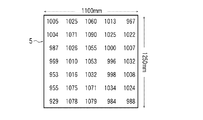
<実施例>
上述した成膜装置1を用い、 幅1100mm、長さl250mm、厚さ0.7mmのガラス基板5を加熱せずに30秒間スパッタリングを行い、基板5表面に膜厚1000Å(100nm)のITO(インジウム錫酸化物)膜を形成した。
<Example>
Using the
ここでは、In2O3-10wt%SnO2(ITO)からなり、幅200mm、長さ1700mm、厚さ10mmのターゲット31a〜31fを6枚用い、各ターゲット31a〜31fを基板5の幅方向に平行に、距離sが2mmになるように配置した。磁界形成手段40a〜40fの幅はターゲット31a〜31fと同じ200mmであった。ガス供給系13からスパッタガスであるArガスを200sccm供給すると共に、反応性ガス(H2O、O2)も供給し、最適流量をコントロールするために、各反応性ガスの流量を0sccm以上5sccm以下の間で変化させ、0.7Paの成膜雰囲気を形成した。交流電圧の印加は、出力を0kwから徐々に上げていき、最終的に20kwまで投入した。交流電圧の周波数は50kHzであった。
Here, six
成膜されたITO膜の膜厚を35点で測定した。その測定結果を図5に示す。
図5に示すように基板5面内の膜厚の偏りは小さく、膜厚分布は35点測定で士8%と良好な値が得られた。このことから、スパッタ中にはプラズマの偏りが小さかったことがわかる。また、スパッタリングの際には異常放電が見られず、放電も安定しており、成膜された膜に混入するパーティクルも殆ど見られなかった。
The film thickness of the deposited ITO film was measured at 35 points. The measurement results are shown in FIG.
As shown in FIG. 5, the deviation of the film thickness within the surface of the
また、反応性ガスとしてO2ガスを用いず、H2Oガスのみを用い、H2Oガスの流量を0sccmから5sccmまで変化させた以外は上記実施例と同じ条件で成膜を行い、ITO膜を形成し、成膜直後のITO膜のシート抵抗(Ω/□)と、成膜後に加熱処理(アニール化処理)したもののシート抵抗(Ω/□)とをそれぞれ測定したところ、成膜直後ではガス流量を変えた場合でもシート抵抗は変わらず、高い値を示した。アニール化をした場合では成膜直後の場合に比べてシート抵抗の値が低く、特にH2Oガスの流量が2sccmの時が最もシート抵抗が低かった。 Further, without using the O 2 gas as a reactive gas, using only the H 2 O gas, subjected to deposition the flow rate of the H 2 O gas under the same conditions as in Example Except for changing from 0sccm to 5 sccm, ITO After forming the film, the sheet resistance (Ω / □) of the ITO film immediately after the film formation and the sheet resistance (Ω / □) of the heat treatment (annealing treatment) after the film formation were measured. Then, even when the gas flow rate was changed, the sheet resistance did not change and showed a high value. In the case of annealing, the sheet resistance value was lower than that immediately after film formation, and the sheet resistance was lowest when the flow rate of H 2 O gas was 2 sccm.
更に、反応性ガスとしてH2OガスとO2ガスの両方を用い、H2Oガスの流量を2sccmに固定し、O2ガスの流量を0から2.0sccmの間で変化させてITO膜の成膜を行い、成膜直後とアニール化処理後でシート抵抗(Ω/□)を測定したところ、成膜直後よりもアニール化処理後でシート抵抗が低くなり、特に、O2ガスの流量が1.0sccmの時が最もシート抵抗が低くなった。従って、反応性ガスの最適流量は、H2Oガスが2sccm、O2 ガスが1sccmであることがわかる。 Further, both H 2 O gas and O 2 gas are used as reactive gases, the flow rate of H 2 O gas is fixed at 2 sccm, and the flow rate of O 2 gas is changed between 0 and 2.0 sccm to form an ITO film. When the sheet resistance (Ω / □) was measured immediately after the film formation and after the annealing treatment, the sheet resistance was lower after the annealing treatment than immediately after the film formation, and in particular, the flow rate of O 2 gas. Was 1.0 sccm, the sheet resistance was the lowest. Therefore, it can be seen that the optimum flow rate of the reactive gas is 2 sccm for H 2 O gas and 1 sccm for O 2 gas.
更に、反応性ガスの流量が最適流量であった場合の、ITO膜のシート抵抗分布を求めたところ、シート抵抗の最大値は26.8Ω/□であり、最小値は23.4Ω/□であり、平均値は25.1Ω/□であり、シート抵抗分布は±6.7%であった。このことから、本発明の成膜装置1を用いれば、シート抵抗分布の良好なITO膜を得られ、そのシート抵抗分布はターゲットの形状や配置を反映したような分布にはならないことがわかる。
Furthermore, when the sheet resistance distribution of the ITO film was obtained when the flow rate of the reactive gas was the optimum flow rate, the maximum value of the sheet resistance was 26.8Ω / □, and the minimum value was 23.4Ω / □. Yes, the average value was 25.1 Ω / □, and the sheet resistance distribution was ± 6.7%. From this, it can be seen that if the
更に、本発明の成膜装置1で長時間成膜を行った場合でも、放電は安定し異常放電は見られなかった。放電後にITOターゲット31a〜31f表面を確認したところ、ターゲット31a〜31f表面に非エロージョン領域は確認されなかった。
Furthermore, even when film formation was performed for a long time with the
<比較例>
成膜装置として、上述した成膜装置1の磁界形成手段40a〜40fに変え、ターゲット31a〜31fよりも幅狭(130mm幅)の棒状磁石を配置し、ターゲットの幅方向に80mm揺動し、ターゲット表面磁場が時間的に変化するよう外部より制御を行った。棒状磁石の揺動速度はlOmm/secの等速反転制御を行った。
<Comparative example>
As the film forming apparatus, instead of the magnetic field forming means 40a to 40f of the
ターゲット31a〜31fは上記実施例と同じものを用い、同じ間隔を空けて配置した。成膜雰囲気はガス供給系13からArガスを200sccm供給し、0.7Paの圧力とした。周波数50kHzで隣接するターゲット31a〜31fの電位を正負に切り替え、電力をOkwから徐々に上げていったところ、lOkwの電力を投入した際にターゲット上で激しい異常放電が目視で確認され、それ以上の電力を投入することができなくなってしまった。放電テスト後、真空槽内を確認したところ、シールド11において異常放電痕が確認された。以上のことから、本発明の成膜装置1を用いれば、スパッタの際に異常放電が起こらず、また、ターゲットに非エロージョン領域も形成されないことがわかる。
The
以上は、隣合うターゲット31a〜31bに同じ交流電源17a〜17cから交流電圧を印加する場合について説明したが、本発明はこれに限定されるものではない。図4に示すように、隣接しない異なる2つのターゲット31a〜31fに、同じ交流電源17a〜17cから交流電圧を印加することもできる。この場合も、隣接するターゲット31a〜31fに異なる極性の電位に交互に置かれるように電圧を印加することが好ましい。
The above has described the case where an AC voltage is applied to the
以上はITOからなる透明導電膜について説明したが、本発明の成膜装置の成膜目的は特に限定されず、金属薄膜、透明導電膜、誘電体膜等種々の膜を成膜し、液晶、PDP(Plasma display panel)もしくはFED(Field Emission Display)もしくはEL(Electro Luminescence)等のフラットパネルディスプレイの製造に用いることができる。 Although the transparent conductive film made of ITO has been described above, the film forming purpose of the film forming apparatus of the present invention is not particularly limited, and various films such as a metal thin film, a transparent conductive film, and a dielectric film are formed, liquid crystal, It can be used for the production of flat panel displays such as PDP (Plasma display panel), FED (Field Emission Display) or EL (Electro Luminescence).
本発明に用いる基板5は特に限定されるものではなく、ガラス基板、樹脂膜付き基板、又は樹脂基板等種々のものを用いることができる。本発明によれば、複数のターゲット31a〜31fを用いることで、成膜面積が広くなるので、平面形状の面積が1m2以上の大型基板の表面に薄膜を形成することができる。
The board |
磁界形成手段40a〜40fをターゲット31a〜31fと同じ真空槽2内部に配置する場合には、磁石42a〜42f、43a〜43f及びヨーク41a〜41fの表面に、スパッタ成膜された膜質に影響を及ぼさないような材質や、表面処理、およびヨーク材との接着方法を施してあることが好ましい。さらに、放電空間と同等の雰囲気中であるため、磁界形成手段40a〜40fのS極、N極間の空間にてプラズマが生成されないように、非磁性体でかつスパッタ成膜された膜質に影響を及ぼさないような表面処理を施してある材料でS極、N極間の空間が満たすことが好ましい。
When the magnetic field forming means 40a to 40f are arranged in the
以上は、磁性体36a〜36fが電極35a〜35fの内部に配置された場合について説明したが、本発明はこれに限定されるものではなく、上述した図6に示したような磁場形状の磁力線が形成されるのであれば、例えば磁性体36a〜36fを配置しなくても良く、また、磁性体36a〜36fを配置する場合にも、その位置は特に限定されるものではなく、例えば磁性体36a〜36fを第一、第二の磁石42ab〜42f、43a〜43fと同じヨーク41a〜41fの上に配置してもよい。
The above has described the case where the
また、上述した図6に示したような磁場形状の磁力線が形成されるのであれば第一、第二の磁石42a〜42f、43a〜43fの形状や配置や数も特に限定されるものではない。
In addition, the shape, arrangement, and number of the first and
各ターゲット31a〜31fの長さは、成膜する基板の長さ以上であり、その一例は1500mm以上2000mm以下である。また、各ターゲット31a〜31fの幅の一例は100mm以上400mm以下である。
The length of each
ターゲットの台数の一例は、ターゲット台数×ターゲット幅十ターゲット台数×ターゲット間距離で表されるカソード外形Wが、基板の幅以上になる台数であり、その一例は1200mm≦W≦1900mmになる台数である。 An example of the number of targets is a number in which the cathode outer shape W expressed by the number of targets × target width + ten target number × distance between targets is equal to or greater than the width of the substrate, and one example is a number satisfying 1200 mm ≦ W ≦ 1900 mm. is there.
隣合うターゲット31a〜31fの互いに対向する側面の距離sの一例は、1mm以上10mm以下である。ターゲット31a〜31fのスパッタ面から基板5の成膜面までの距離の一例は60mm以上300mm以下である。
An example of the distance s between the side surfaces of the
ターゲット31a〜31fのスパッタ面は同じ平面上に配置されることが好ましい。ターゲット31a〜31fの厚さは特に限定されるものではないが、その一例は5mm以上30mm以下である。
The sputtering surfaces of the
電極35a〜35fに冷却手段を取り付ければ、ターゲット31a〜31fを冷却しながらスパッタリングを行うことができる。ターゲット31a〜31fを取り付ける電極35a〜35fの厚さは特に限定されるものではないが、その一例は5mm以上30mm以下である。
If a cooling means is attached to the
ターゲット31a〜31f及び電極35a〜35fを、磁界形成手段40a〜40fから電気的に絶縁する絶縁板33a〜33fの厚さの一例は、2mm以上10mm以下である。
An example of the thickness of the insulating
また、真空槽2内部にターゲット31a〜31fの長手方向に沿って、ガス管を配置し、該ガス管によって隣接するターゲット31a〜31fの間からスパッタガスや反応ガスを流せば、放電空間に直接ガスが供給されるので、ガスの供給律速におちいりにくくなる。この場合、基板の側面の周囲に排気口を設ければ、放電空間に供給されたガスが速やかに排気される。
Further, if a gas pipe is disposed in the
ターゲット31a〜31fへの電力供給の一例は、1つの交流電源17a〜17cに接続された2つのターゲット31a〜31fに対して、その出力密度Pが、1W/cm2以上10W/cm2以下である。また、金属ターゲット31a〜31fを用いる場合には、出力密度Pの一例は5W/cm2以上40W/cm2である。
An example of power supply to the
また、ターゲット31a〜31fへの電力供給の一例は、基板上の膜厚の分布を調整するために、複数並べらたターゲット31a〜31fのうち、最も外側に位置するターゲット31a、31fへの供給が、中央位置にあるターゲット31c、31dへの供給量の100%以上130%以下となるように供給する。
In addition, as an example of power supply to the
また、スパッタリングの際には、ターゲット31a〜31fに印加する電圧の一例は、接地電位に対して−3000V以上の交流電圧である。
Moreover, in sputtering, an example of a voltage applied to the
以上は1つの補助磁界形成手段15a、15bを1つの細長の磁石で構成する場合について説明したが、本発明はこれに限定されるものではなく、1つの補助磁界形成手段を複数個の磁石で構成し、各磁石をターゲットの長手方向に沿って、磁界形成手段の配置された領域の外側に配置してもよい。また、補助磁界形成手段15a、15bと、隣接する第一の磁石42a、42fが密着している場合には、これらの磁石を一体成形してもよい。
In the above, the case where one auxiliary magnetic
上述した成膜装置1では、磁界形成手段40a〜40bと補助磁界形成手段15a、15bを移動させずにスパッタリングを続けても、ターゲット31a〜31fのほぼ全面がスパッタされるが、ターゲット31a〜31f表面上の磁束密度が均一ではないと、磁束密度が高い部分と低い部分でスパッタリングによる膜厚減少量に差が生じてしまう。
In the
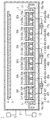
この問題を解決するための本発明第二例の成膜装置を図9に示す。この成膜装置7は、磁性体36a〜36f以外の上記成膜装置1の構成を全て有している。成膜装置7は、更に移動手段14を有しており、各磁界形成手段40a〜40fと、各補助磁界形成手段15a、15bは、移動手段14に接続され、移動手段14と一緒に移動するようになっている。
移動手段14は不図示のモータによって、ターゲット31a〜31fの表面に対して平行な面内で、ターゲット31a〜31fに対して相対的に移動するように構成されているので、各磁界形成手段40a〜40fと、各補助磁界形成手段15a、15bも、ターゲット31a〜31fの表面に対して平行な面内で移動する。
FIG. 9 shows a film forming apparatus according to a second example of the present invention for solving this problem. This film-forming
Since the moving
従って、ターゲット31a〜31fの平面と、磁界形成手段40a〜40fの平面との距離は変わらない。また、各磁界形成手段40a〜40fと各補助磁界形成手段15a、15bは同じ移動手段14に固定されていて、移動手段14に対して静止しているから、各磁界形成手段40a〜40fと、各補助磁界形成手段15a、15bの相対的な位置関係は変わりがない。従って、ターゲット31a〜31f表面上の磁束密度の形状には変化はないが、磁束密度の形状とターゲット31a〜31f表面の相対的な位置関係が変化する。
Therefore, the distance between the plane of the
ここでは移動手段14の移動方向は、ターゲット31a〜31fの並べられた方向に沿っており、従って磁界形成手段40a〜40fと補助磁界形成手段15a、15bは、ターゲット31a〜31fの並べられた方向に沿って移動する。
図10(a)は磁界形成手段40a〜40fが対応するターゲット31a〜31fの真裏位置に配置された初期状態を示しており、移動手段14が移動すると、図10(b)に示すように、磁界形成手段40a〜40bが対応するターゲット31a〜31fの真裏位置からずれ、列の先頭又は終わりのターゲット31a、31fの端部が磁界形成手段40a〜40fの列からはみ出した状態になるが、移動によってその端部の真下位置には補助磁界形成手段15a、15bが近づくので、結局、各ターゲット31a〜31fの表面には、移動方向の一端から他端まで磁力線が通る。
Here, the moving direction of the moving
FIG. 10A shows an initial state in which the magnetic field forming means 40a to 40f are arranged at the positions directly behind the corresponding
次に、この成膜装置7を用いて成膜を行う工程について説明する。
成膜終了後の基板5と新たな基板5とを交換する間に、磁界形成手段40a〜40fと補助磁界形成手段15a、15bを、上記対応するターゲット31a〜31fに隣接するターゲット31a〜31fの真裏位置に、磁界形成手段40a〜40fが入り込まない移動量Dで移動させ、新たな基板5の表面に成膜を行う際には、磁界形成手段40a〜40fと補助磁界形成手段15a、15とを、ターゲット31a〜31fに対して静止させてスパッタリングを行う。
Next, a process of forming a film using this
While exchanging the
磁界の形状とターゲット31a〜31f表面の位置関係が変化すると、ターゲット31a〜31f表面上の磁束密度の高い部分が移動するので、ターゲット31a〜31fの膜厚減少量の少なかった部分が多くスパッタされ、逆に膜厚減少量が多かった部分が少なくスパッタされる。
磁界形成手段40a〜40fと補助磁界形成手段15a、15bの移動と、ターゲット31a〜31fのスパッタリングとを繰り返せば、ターゲット31a〜31fの表面が均一に膜厚減少するので、ターゲット31a〜31fの使用効率が高い。
When the positional relationship between the shape of the magnetic field and the surfaces of the
If the movement of the magnetic field forming means 40a to 40f and the auxiliary magnetic field forming means 15a and 15b and the sputtering of the
尚、図1の成膜装置1ではスパッタ部30a〜30fに磁性体36a〜36fを配置することで、ターゲット31a〜31f表面での磁束密度が均一になり、ターゲット31a〜31fの膜厚減少が均一になっていたが、第二例の成膜装置7では磁性体36a〜36fが無くても、磁界形成手段40a〜40fと補助磁界形成手段15a、15fを移動させることで、結果的にターゲット31a〜31fの膜厚減少量が均一になる。
In addition, in the film-forming
以上は、磁界形成手段40a〜40fと、補助磁界形成手段15a、15bを一緒に移動させる場合について説明したが、本発明はこれに限定されず、ターゲット31a〜31fがスパッタされる時に、各磁界形成手段40a〜40fと各補助磁界形成手段15a、15bが、互いの相対的な位置関係を変えずに、ターゲット31a〜31fに対する相対的な位置関係を変えているのであれば、各磁界形成手段40a〜40fと各補助磁界形成手段15a、15bを別々に移動させても良い。
また、磁界形成手段40a〜40fと補助磁界形成手段15a、15bを静止させ、ターゲット31a〜31fを移動させてもよいし、磁界形成手段40a〜40fと補助磁界形成手段15a、15bを互いの相対的な位置関係を変化させずに移動させると共に、ターゲット31a〜31fを移動させても良い。
In the above, the case where the magnetic field forming means 40a to 40f and the auxiliary magnetic field forming means 15a and 15b are moved together has been described. However, the present invention is not limited to this, and each magnetic field is generated when the
Further, the magnetic field forming means 40a to 40f and the auxiliary magnetic field forming means 15a and 15b may be stationary, and the
1……成膜装置 2……真空槽 3……スパッタ源 4……基板ホルダ 5……基板 15a、15b……補助磁界形成手段 17a〜17c……交流電源 30a〜30f……スパッタ部 31a〜31f……ターゲット 40a〜40f……磁界形成手段 42a〜42f……第一の磁石 43a〜43f……第二の磁石
DESCRIPTION OF
Claims (6)
前記複数のターゲットのうち、異なるターゲットに同じ交流電源から極性が異なる交流電圧が印加され、
前記複数のターゲットはスパッタ面が同じ方向に向けられた状態で、隣合う前記ターゲットの長手方向の側面が、前記真空槽中の雰囲気のみを介して互いに直接対向するように配置された成膜装置。 A vacuum chamber, a plate-like target having a plurality of longitudinal directions, and an AC power source for applying an AC voltage to the target,
Among the plurality of targets, AC voltages having different polarities are applied to different targets from the same AC power source,
The film forming apparatus in which the plurality of targets are arranged such that the side surfaces in the longitudinal direction of the adjacent targets are directly opposed to each other only through the atmosphere in the vacuum chamber with the sputtering surfaces directed in the same direction. .
前記各ターゲットは長手方向の側面同士が対向するように互いに平行に配置され、
前記各ターゲットの真裏位置には、細長の磁界形成手段が前記ターゲットの長手方向に沿ってそれぞれ配置され、
前記磁界形成手段が配置された領域の外側であって、前記ターゲットの真裏位置よりも外側には、細長の補助磁界形成手段が前記ターゲットの長手方向に沿って配置された成膜装置。 Having a vacuum chamber and a plurality of elongated plate-like targets arranged inside the vacuum chamber;
The targets are arranged in parallel to each other so that the side surfaces in the longitudinal direction face each other.
Elongated magnetic field forming means are respectively arranged along the longitudinal direction of the target at the position directly behind each target,
A film forming apparatus in which elongated auxiliary magnetic field forming means is arranged along the longitudinal direction of the target outside the region where the magnetic field forming means is arranged and outside the position directly behind the target.
前記複数の磁石のうち、前記補助磁界形成手段に隣接して配置された磁石の前記ターゲット側に向けられた面の磁極は、前記補助磁界形成手段の前記ターゲット側に向けられた面の磁極と同じ極性にされた請求項4記載の成膜装置。 Each of the magnetic field forming means has a plurality of magnets,
Of the plurality of magnets, the magnetic pole of the surface of the magnet disposed adjacent to the auxiliary magnetic field forming unit is directed to the target side, and the magnetic pole of the surface directed to the target side of the auxiliary magnetic field forming unit is The film-forming apparatus of Claim 4 made into the same polarity.
Priority Applications (4)
| Application Number | Priority Date | Filing Date | Title |
|---|---|---|---|
| JP2005040668A JP4780972B2 (en) | 2004-03-11 | 2005-02-17 | Sputtering equipment |
| TW094105312A TWI375729B (en) | 2004-03-11 | 2005-02-22 | Sputtering apparatus |
| CN2005100527186A CN1667155B (en) | 2004-03-11 | 2005-03-10 | Sputtering device |
| KR1020050020100A KR101164047B1 (en) | 2004-03-11 | 2005-03-10 | Sputtering apparatus |
Applications Claiming Priority (3)
| Application Number | Priority Date | Filing Date | Title |
|---|---|---|---|
| JP2004069413 | 2004-03-11 | ||
| JP2004069413 | 2004-03-11 | ||
| JP2005040668A JP4780972B2 (en) | 2004-03-11 | 2005-02-17 | Sputtering equipment |
Publications (2)
| Publication Number | Publication Date |
|---|---|
| JP2005290550A true JP2005290550A (en) | 2005-10-20 |
| JP4780972B2 JP4780972B2 (en) | 2011-09-28 |
Family
ID=35038430
Family Applications (1)
| Application Number | Title | Priority Date | Filing Date |
|---|---|---|---|
| JP2005040668A Expired - Lifetime JP4780972B2 (en) | 2004-03-11 | 2005-02-17 | Sputtering equipment |
Country Status (4)
| Country | Link |
|---|---|
| JP (1) | JP4780972B2 (en) |
| KR (1) | KR101164047B1 (en) |
| CN (1) | CN1667155B (en) |
| TW (1) | TWI375729B (en) |
Cited By (22)
| Publication number | Priority date | Publication date | Assignee | Title |
|---|---|---|---|---|
| WO2007080906A1 (en) * | 2006-01-11 | 2007-07-19 | Ulvac, Inc. | Sputtering apparatus |
| WO2008050618A1 (en) * | 2006-10-24 | 2008-05-02 | Ulvac, Inc. | Thin film forming method and thin film forming device |
| JP2008274366A (en) * | 2007-05-01 | 2008-11-13 | Ulvac Japan Ltd | Sputtering apparatus and sputtering method |
| JP2009041082A (en) * | 2007-08-10 | 2009-02-26 | Ulvac Japan Ltd | Thin film formation method |
| WO2009025306A1 (en) * | 2007-08-20 | 2009-02-26 | Ulvac, Inc. | Sputtering method |
| WO2009025258A1 (en) * | 2007-08-20 | 2009-02-26 | Ulvac, Inc. | Sputtering method and sputtering apparatus |
| WO2009028552A1 (en) * | 2007-08-31 | 2009-03-05 | Ulvac, Inc. | Sputtering apparatus |
| JP2009280890A (en) * | 2008-05-26 | 2009-12-03 | Ulvac Japan Ltd | Sputtering method |
| WO2010090197A1 (en) * | 2009-02-04 | 2010-08-12 | シャープ株式会社 | Object coated with transparent conductive film and process for producing same |
| JP2010236051A (en) * | 2009-03-31 | 2010-10-21 | Ulvac Japan Ltd | Sputtering method |
| CN102677008A (en) * | 2012-05-14 | 2012-09-19 | 深圳市创益科技发展有限公司 | Online preparation of coating of electric conduction electrode of solar battery |
| JP2012184479A (en) * | 2011-03-07 | 2012-09-27 | Ulvac Japan Ltd | Sputtering apparatus and sputtering method |
| JP2013067855A (en) * | 2011-09-06 | 2013-04-18 | Idemitsu Kosan Co Ltd | Sputtering target |
| US20130098757A1 (en) * | 2010-06-17 | 2013-04-25 | Ulvac, Inc. | Sputtering deposition apparatus and adhesion preventing member |
| CN103184422A (en) * | 2013-03-25 | 2013-07-03 | 肇庆市腾胜真空技术工程有限公司 | Low-temperature deposition device and process for TCO film |
| CN103354241A (en) * | 2010-12-28 | 2013-10-16 | 出光兴产株式会社 | Laminated structure having oxide semiconductor thin film layer, method of manufacturing laminated structure, thin film transistor, and display device |
| WO2014080815A1 (en) * | 2012-11-20 | 2014-05-30 | 株式会社 アルバック | Sputtering apparatus |
| WO2014112376A1 (en) * | 2013-01-16 | 2014-07-24 | 出光興産株式会社 | Sputtering target, oxide semiconductor thin film, and thin film transistor comprising said oxide semiconductor thin film |
| JP2014524516A (en) * | 2011-08-25 | 2014-09-22 | アプライド マテリアルズ インコーポレイテッド | Sputtering apparatus and sputtering method |
| JP2014218706A (en) * | 2013-05-09 | 2014-11-20 | 出光興産株式会社 | Sputtering target, oxide semiconductor thin film, and manufacturing method of them |
| US9210788B2 (en) | 2008-06-30 | 2015-12-08 | Ulvac, Inc. | Power supply apparatus |
| WO2019003809A1 (en) * | 2017-06-30 | 2019-01-03 | 凸版印刷株式会社 | Film treatment method and film production method |
Families Citing this family (6)
| Publication number | Priority date | Publication date | Assignee | Title |
|---|---|---|---|---|
| JP4963023B2 (en) * | 2006-01-11 | 2012-06-27 | 株式会社アルバック | Sputtering method and sputtering apparatus |
| CN102312206B (en) * | 2010-06-29 | 2015-07-15 | 株式会社爱发科 | Sputtering method |
| WO2016017510A1 (en) * | 2014-07-31 | 2016-02-04 | 株式会社 アルバック | Substrate processing device |
| KR102053400B1 (en) * | 2017-07-07 | 2020-01-07 | 주식회사 에이치앤이루자 | Sputtering device including magnetic flux block |
| CN109487225A (en) * | 2019-01-07 | 2019-03-19 | 成都中电熊猫显示科技有限公司 | Magnetron sputtering film formation device and method |
| CN114318269B (en) * | 2022-01-05 | 2022-10-28 | 中国科学院兰州化学物理研究所 | Device and method for sputtering and depositing metal on surface of magnetic powder material |
Citations (5)
| Publication number | Priority date | Publication date | Assignee | Title |
|---|---|---|---|---|
| JPS61270366A (en) * | 1985-05-23 | 1986-11-29 | Nec Corp | Tripolar sputtering source |
| JPH02156080A (en) * | 1988-12-09 | 1990-06-15 | Tokuda Seisakusho Ltd | sputtering equipment |
| JPH05148644A (en) * | 1991-11-26 | 1993-06-15 | Asahi Glass Co Ltd | Sputtering device |
| JP2001140069A (en) * | 1999-11-12 | 2001-05-22 | Anelva Corp | Magnetron cathode for sputtering equipment |
| JP2001262335A (en) * | 2000-03-21 | 2001-09-26 | Nippon Sheet Glass Co Ltd | Film coating method |
Family Cites Families (1)
| Publication number | Priority date | Publication date | Assignee | Title |
|---|---|---|---|---|
| JPH0835064A (en) * | 1994-07-20 | 1996-02-06 | Matsushita Electric Ind Co Ltd | Sputtering equipment |
-
2005
- 2005-02-17 JP JP2005040668A patent/JP4780972B2/en not_active Expired - Lifetime
- 2005-02-22 TW TW094105312A patent/TWI375729B/en not_active IP Right Cessation
- 2005-03-10 CN CN2005100527186A patent/CN1667155B/en not_active Expired - Lifetime
- 2005-03-10 KR KR1020050020100A patent/KR101164047B1/en not_active Expired - Lifetime
Patent Citations (5)
| Publication number | Priority date | Publication date | Assignee | Title |
|---|---|---|---|---|
| JPS61270366A (en) * | 1985-05-23 | 1986-11-29 | Nec Corp | Tripolar sputtering source |
| JPH02156080A (en) * | 1988-12-09 | 1990-06-15 | Tokuda Seisakusho Ltd | sputtering equipment |
| JPH05148644A (en) * | 1991-11-26 | 1993-06-15 | Asahi Glass Co Ltd | Sputtering device |
| JP2001140069A (en) * | 1999-11-12 | 2001-05-22 | Anelva Corp | Magnetron cathode for sputtering equipment |
| JP2001262335A (en) * | 2000-03-21 | 2001-09-26 | Nippon Sheet Glass Co Ltd | Film coating method |
Cited By (43)
| Publication number | Priority date | Publication date | Assignee | Title |
|---|---|---|---|---|
| KR101018652B1 (en) * | 2006-01-11 | 2011-03-04 | 가부시키가이샤 알박 | Sputtering device |
| WO2007080906A1 (en) * | 2006-01-11 | 2007-07-19 | Ulvac, Inc. | Sputtering apparatus |
| US8460522B2 (en) | 2006-10-24 | 2013-06-11 | Ulvac, Inc. | Method of forming thin film and apparatus for forming thin film |
| WO2008050618A1 (en) * | 2006-10-24 | 2008-05-02 | Ulvac, Inc. | Thin film forming method and thin film forming device |
| JP5162464B2 (en) * | 2006-10-24 | 2013-03-13 | 株式会社アルバック | Thin film forming method and thin film forming apparatus |
| JP2008274366A (en) * | 2007-05-01 | 2008-11-13 | Ulvac Japan Ltd | Sputtering apparatus and sputtering method |
| WO2008136337A1 (en) * | 2007-05-01 | 2008-11-13 | Ulvac, Inc. | Sputtering apparatus and sputtering method |
| KR101050121B1 (en) * | 2007-05-01 | 2011-07-19 | 가부시키가이샤 알박 | Sputtering Device and Sputtering Method |
| JP2009041082A (en) * | 2007-08-10 | 2009-02-26 | Ulvac Japan Ltd | Thin film formation method |
| JP5322234B2 (en) * | 2007-08-20 | 2013-10-23 | 株式会社アルバック | Sputtering method and sputtering apparatus |
| JP5322235B2 (en) * | 2007-08-20 | 2013-10-23 | 株式会社アルバック | Sputtering method |
| WO2009025258A1 (en) * | 2007-08-20 | 2009-02-26 | Ulvac, Inc. | Sputtering method and sputtering apparatus |
| WO2009025306A1 (en) * | 2007-08-20 | 2009-02-26 | Ulvac, Inc. | Sputtering method |
| JP2009057608A (en) * | 2007-08-31 | 2009-03-19 | Ulvac Japan Ltd | Sputtering device |
| WO2009028552A1 (en) * | 2007-08-31 | 2009-03-05 | Ulvac, Inc. | Sputtering apparatus |
| KR101196650B1 (en) | 2007-08-31 | 2012-11-02 | 가부시키가이샤 알박 | Sputtering apparatus |
| KR101250336B1 (en) | 2008-05-26 | 2013-04-03 | 가부시키가이샤 알박 | Sputtering method |
| WO2009145093A1 (en) * | 2008-05-26 | 2009-12-03 | 株式会社アルバック | Sputtering method |
| US8404089B2 (en) | 2008-05-26 | 2013-03-26 | Ulvac, Inc. | Sputtering method |
| JP2009280890A (en) * | 2008-05-26 | 2009-12-03 | Ulvac Japan Ltd | Sputtering method |
| US9210788B2 (en) | 2008-06-30 | 2015-12-08 | Ulvac, Inc. | Power supply apparatus |
| WO2010090197A1 (en) * | 2009-02-04 | 2010-08-12 | シャープ株式会社 | Object coated with transparent conductive film and process for producing same |
| JP2010236051A (en) * | 2009-03-31 | 2010-10-21 | Ulvac Japan Ltd | Sputtering method |
| US20130098757A1 (en) * | 2010-06-17 | 2013-04-25 | Ulvac, Inc. | Sputtering deposition apparatus and adhesion preventing member |
| US8785927B2 (en) | 2010-12-28 | 2014-07-22 | Idemitsu Kosan Co., Ltd. | Laminate structure including oxide semiconductor thin film layer, and thin film transistor |
| CN103354241A (en) * | 2010-12-28 | 2013-10-16 | 出光兴产株式会社 | Laminated structure having oxide semiconductor thin film layer, method of manufacturing laminated structure, thin film transistor, and display device |
| CN103400751A (en) * | 2010-12-28 | 2013-11-20 | 出光兴产株式会社 | Manufacturing method of laminated structure having oxide semiconductor thin film layer |
| EP2660868A4 (en) * | 2010-12-28 | 2014-02-19 | Idemitsu Kosan Co | LAMINATE STRUCTURE COMPRISING A THIN OXIDE SEMICONDUCTOR THIN FILM LAYER AND THIN FILM TRANSISTOR |
| JP2012184479A (en) * | 2011-03-07 | 2012-09-27 | Ulvac Japan Ltd | Sputtering apparatus and sputtering method |
| JP2014524516A (en) * | 2011-08-25 | 2014-09-22 | アプライド マテリアルズ インコーポレイテッド | Sputtering apparatus and sputtering method |
| US9767998B2 (en) | 2011-09-06 | 2017-09-19 | Idemitsu Kosan Co., Ltd. | Sputtering target |
| JP2013067855A (en) * | 2011-09-06 | 2013-04-18 | Idemitsu Kosan Co Ltd | Sputtering target |
| CN102677008A (en) * | 2012-05-14 | 2012-09-19 | 深圳市创益科技发展有限公司 | Online preparation of coating of electric conduction electrode of solar battery |
| WO2014080815A1 (en) * | 2012-11-20 | 2014-05-30 | 株式会社 アルバック | Sputtering apparatus |
| WO2014112376A1 (en) * | 2013-01-16 | 2014-07-24 | 出光興産株式会社 | Sputtering target, oxide semiconductor thin film, and thin film transistor comprising said oxide semiconductor thin film |
| JPWO2014112376A1 (en) * | 2013-01-16 | 2017-01-19 | 出光興産株式会社 | Sputtering target, oxide semiconductor thin film, and thin film transistor including the oxide semiconductor thin film |
| JP2018165407A (en) * | 2013-01-16 | 2018-10-25 | 出光興産株式会社 | Sputtering target, oxide semiconductor thin film, and thin film transistor including the oxide semiconductor thin film |
| CN103184422A (en) * | 2013-03-25 | 2013-07-03 | 肇庆市腾胜真空技术工程有限公司 | Low-temperature deposition device and process for TCO film |
| JP2014218706A (en) * | 2013-05-09 | 2014-11-20 | 出光興産株式会社 | Sputtering target, oxide semiconductor thin film, and manufacturing method of them |
| WO2019003809A1 (en) * | 2017-06-30 | 2019-01-03 | 凸版印刷株式会社 | Film treatment method and film production method |
| JPWO2019003809A1 (en) * | 2017-06-30 | 2020-04-23 | 凸版印刷株式会社 | Film processing method and film manufacturing method |
| US11651944B2 (en) | 2017-06-30 | 2023-05-16 | Toppan Printing Co., Ltd. | Film processing method and film manufacturing method |
| JP7342702B2 (en) | 2017-06-30 | 2023-09-12 | 凸版印刷株式会社 | Film processing method and film manufacturing method |
Also Published As
| Publication number | Publication date |
|---|---|
| CN1667155B (en) | 2010-05-26 |
| TW200538568A (en) | 2005-12-01 |
| KR20060043832A (en) | 2006-05-15 |
| KR101164047B1 (en) | 2012-07-18 |
| JP4780972B2 (en) | 2011-09-28 |
| TWI375729B (en) | 2012-11-01 |
| CN1667155A (en) | 2005-09-14 |
Similar Documents
| Publication | Publication Date | Title |
|---|---|---|
| JP4780972B2 (en) | Sputtering equipment | |
| KR100239818B1 (en) | Apparatus for the reactive coating of a substrate | |
| JP4246547B2 (en) | Sputtering apparatus and sputtering method | |
| US6217714B1 (en) | Sputtering apparatus | |
| KR20010024668A (en) | magnetron sputtering source | |
| JP5004931B2 (en) | Sputtering source, sputtering apparatus, and sputtering method | |
| JP2010537041A (en) | Low impedance plasma | |
| JPH11504988A (en) | Apparatus for reducing arcing during sputtering | |
| JP2009057608A (en) | Sputtering device | |
| JP5322234B2 (en) | Sputtering method and sputtering apparatus | |
| CN101657562B (en) | Sputtering apparatus and sputtering method | |
| JP4580781B2 (en) | Sputtering method and apparatus | |
| KR20170064527A (en) | Magnet unit for magnetron sputter electrode and sputtering apparutus | |
| JP5322235B2 (en) | Sputtering method | |
| KR20110122456A (en) | Manufacturing apparatus and manufacturing method of liquid crystal display | |
| JP2009144234A (en) | Film forming apparatus and film forming method | |
| JP4959175B2 (en) | Magnetron sputtering electrode and sputtering apparatus provided with magnetron sputtering electrode | |
| JPH11350130A (en) | Thin film forming equipment | |
| JP2006188733A (en) | Facing-target type sputtering apparatus and facing-target type sputtering method | |
| JP5025334B2 (en) | Magnetron sputtering electrode and sputtering apparatus provided with magnetron sputtering electrode | |
| JP2007031816A (en) | Sputtering apparatus and sputtering method | |
| CN101897002B (en) | Plasma non-destructive sputtering gun, sputtering device, plasma processing device and film forming method | |
| RU2075539C1 (en) | Device for ionic-plasma spraying of materials in vacuum | |
| JPS63286572A (en) | Planar magnetron type sputtering equipment | |
| KR101683726B1 (en) | apparatus for processing substrates |
Legal Events
| Date | Code | Title | Description |
|---|---|---|---|
| A621 | Written request for application examination |
Free format text: JAPANESE INTERMEDIATE CODE: A621 Effective date: 20071119 |
|
| A977 | Report on retrieval |
Free format text: JAPANESE INTERMEDIATE CODE: A971007 Effective date: 20100324 |
|
| A131 | Notification of reasons for refusal |
Free format text: JAPANESE INTERMEDIATE CODE: A131 Effective date: 20100406 |
|
| A521 | Request for written amendment filed |
Free format text: JAPANESE INTERMEDIATE CODE: A523 Effective date: 20100607 Free format text: JAPANESE INTERMEDIATE CODE: A821 Effective date: 20100607 |
|
| A131 | Notification of reasons for refusal |
Free format text: JAPANESE INTERMEDIATE CODE: A131 Effective date: 20110329 |
|
| A521 | Request for written amendment filed |
Free format text: JAPANESE INTERMEDIATE CODE: A523 Effective date: 20110506 Free format text: JAPANESE INTERMEDIATE CODE: A821 Effective date: 20110506 |
|
| TRDD | Decision of grant or rejection written | ||
| A01 | Written decision to grant a patent or to grant a registration (utility model) |
Free format text: JAPANESE INTERMEDIATE CODE: A01 Effective date: 20110705 |
|
| A01 | Written decision to grant a patent or to grant a registration (utility model) |
Free format text: JAPANESE INTERMEDIATE CODE: A01 |
|
| A61 | First payment of annual fees (during grant procedure) |
Free format text: JAPANESE INTERMEDIATE CODE: A61 Effective date: 20110705 |
|
| FPAY | Renewal fee payment (event date is renewal date of database) |
Free format text: PAYMENT UNTIL: 20140715 Year of fee payment: 3 |
|
| R150 | Certificate of patent or registration of utility model |
Ref document number: 4780972 Country of ref document: JP Free format text: JAPANESE INTERMEDIATE CODE: R150 |
|
| R250 | Receipt of annual fees |
Free format text: JAPANESE INTERMEDIATE CODE: R250 |
|
| R250 | Receipt of annual fees |
Free format text: JAPANESE INTERMEDIATE CODE: R250 |
|
| R250 | Receipt of annual fees |
Free format text: JAPANESE INTERMEDIATE CODE: R250 |
|
| R250 | Receipt of annual fees |
Free format text: JAPANESE INTERMEDIATE CODE: R250 |
|
| R250 | Receipt of annual fees |
Free format text: JAPANESE INTERMEDIATE CODE: R250 |
|
| R250 | Receipt of annual fees |
Free format text: JAPANESE INTERMEDIATE CODE: R250 |
|
| R250 | Receipt of annual fees |
Free format text: JAPANESE INTERMEDIATE CODE: R250 |
|
| R250 | Receipt of annual fees |
Free format text: JAPANESE INTERMEDIATE CODE: R250 |
|
| R250 | Receipt of annual fees |
Free format text: JAPANESE INTERMEDIATE CODE: R250 |
|
| EXPY | Cancellation because of completion of term |