JP2005129909A - 光センサー装置および電子機器 - Google Patents
光センサー装置および電子機器 Download PDFInfo
- Publication number
- JP2005129909A JP2005129909A JP2004269801A JP2004269801A JP2005129909A JP 2005129909 A JP2005129909 A JP 2005129909A JP 2004269801 A JP2004269801 A JP 2004269801A JP 2004269801 A JP2004269801 A JP 2004269801A JP 2005129909 A JP2005129909 A JP 2005129909A
- Authority
- JP
- Japan
- Prior art keywords
- optical sensor
- amplifier circuit
- tft
- photodiode
- sensor device
- Prior art date
- Legal status (The legal status is an assumption and is not a legal conclusion. Google has not performed a legal analysis and makes no representation as to the accuracy of the status listed.)
- Withdrawn
Links
- 230000003287 optical effect Effects 0.000 title claims abstract description 136
- 239000000758 substrate Substances 0.000 claims abstract description 69
- 229910021417 amorphous silicon Inorganic materials 0.000 claims abstract description 25
- 239000010409 thin film Substances 0.000 claims abstract description 24
- 238000006243 chemical reaction Methods 0.000 claims description 40
- 230000003321 amplification Effects 0.000 claims description 9
- 238000003199 nucleic acid amplification method Methods 0.000 claims description 9
- 229910021420 polycrystalline silicon Inorganic materials 0.000 claims description 7
- 229920005591 polysilicon Polymers 0.000 claims description 7
- 239000011521 glass Substances 0.000 claims description 2
- 239000004065 semiconductor Substances 0.000 abstract description 18
- 239000010410 layer Substances 0.000 description 23
- 239000010408 film Substances 0.000 description 12
- 230000007423 decrease Effects 0.000 description 7
- 230000035945 sensitivity Effects 0.000 description 7
- 239000011229 interlayer Substances 0.000 description 6
- 229910021421 monocrystalline silicon Inorganic materials 0.000 description 4
- 230000015572 biosynthetic process Effects 0.000 description 3
- 238000000034 method Methods 0.000 description 3
- 230000000007 visual effect Effects 0.000 description 3
- 230000005540 biological transmission Effects 0.000 description 2
- 230000003247 decreasing effect Effects 0.000 description 2
- 230000006866 deterioration Effects 0.000 description 2
- 239000013081 microcrystal Substances 0.000 description 2
- 229910021424 microcrystalline silicon Inorganic materials 0.000 description 2
- 206010034972 Photosensitivity reaction Diseases 0.000 description 1
- 239000003990 capacitor Substances 0.000 description 1
- 238000004891 communication Methods 0.000 description 1
- 239000004020 conductor Substances 0.000 description 1
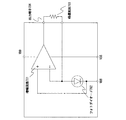
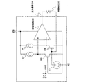
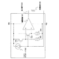
- 238000010586 diagram Methods 0.000 description 1
- 238000005516 engineering process Methods 0.000 description 1
- AMGQUBHHOARCQH-UHFFFAOYSA-N indium;oxotin Chemical compound [In].[Sn]=O AMGQUBHHOARCQH-UHFFFAOYSA-N 0.000 description 1
- 230000007774 longterm Effects 0.000 description 1
- 239000000463 material Substances 0.000 description 1
- 230000036211 photosensitivity Effects 0.000 description 1
- 229920001690 polydopamine Polymers 0.000 description 1
- 230000000630 rising effect Effects 0.000 description 1
Images


Landscapes
- Light Receiving Elements (AREA)
- Solid State Image Pick-Up Elements (AREA)
- Thin Film Transistor (AREA)
Priority Applications (1)
| Application Number | Priority Date | Filing Date | Title |
|---|---|---|---|
| JP2004269801A JP2005129909A (ja) | 2003-09-19 | 2004-09-16 | 光センサー装置および電子機器 |
Applications Claiming Priority (3)
| Application Number | Priority Date | Filing Date | Title |
|---|---|---|---|
| JP2003327629 | 2003-09-19 | ||
| JP2003342632 | 2003-09-30 | ||
| JP2004269801A JP2005129909A (ja) | 2003-09-19 | 2004-09-16 | 光センサー装置および電子機器 |
Related Child Applications (1)
| Application Number | Title | Priority Date | Filing Date |
|---|---|---|---|
| JP2010244928A Division JP5542259B2 (ja) | 2003-09-19 | 2010-11-01 | 光センサー装置 |
Publications (2)
| Publication Number | Publication Date |
|---|---|
| JP2005129909A true JP2005129909A (ja) | 2005-05-19 |
| JP2005129909A5 JP2005129909A5 (https=) | 2007-10-25 |
Family
ID=34657715
Family Applications (1)
| Application Number | Title | Priority Date | Filing Date |
|---|---|---|---|
| JP2004269801A Withdrawn JP2005129909A (ja) | 2003-09-19 | 2004-09-16 | 光センサー装置および電子機器 |
Country Status (1)
| Country | Link |
|---|---|
| JP (1) | JP2005129909A (https=) |
Cited By (12)
| Publication number | Priority date | Publication date | Assignee | Title |
|---|---|---|---|---|
| JP2008227476A (ja) * | 2007-02-15 | 2008-09-25 | Semiconductor Energy Lab Co Ltd | 光電変換装置及び電子機器、並びに光電変換装置の作製方法 |
| WO2009014155A1 (en) * | 2007-07-25 | 2009-01-29 | Semiconductor Energy Laboratory Co., Ltd. | Photoelectric conversion device and electronic device having the same |
| JP2009246347A (ja) * | 2008-03-14 | 2009-10-22 | Semiconductor Energy Lab Co Ltd | 半導体装置 |
| US7622785B2 (en) | 2006-04-28 | 2009-11-24 | Semiconductor Laboratory Co., Ltd. | Photoelectric conversion element and manufacturing method of photoelectric conversion element |
| US8053717B2 (en) | 2008-05-22 | 2011-11-08 | Semiconductor Energy Laboratory Co., Ltd. | Photoelectric conversion device having a reference voltage generation circuit with a resistor and a second diode element and electronic device having the same |
| US8053816B2 (en) | 2006-03-10 | 2011-11-08 | Semiconductor Energy Laboratory Co., Ltd. | Semiconductor device |
| US8431883B2 (en) | 2007-06-29 | 2013-04-30 | Semiconductor Energy Laboratory Co., Ltd. | Photoelectric conversion device comprising a current mirror circuit connected to a field effect transistor, a buffer and a voltage detection circuit |
| WO2013065668A1 (ja) * | 2011-10-31 | 2013-05-10 | 京セラ株式会社 | 受発光一体型素子を用いた受発光装置およびセンサ装置 |
| US8610226B2 (en) | 2009-12-28 | 2013-12-17 | Sharp Kabushiki Kaisha | Photosensor element, photosensor circuit, thin-film transistor substrate, and display panel |
| US8614493B2 (en) | 2009-12-25 | 2013-12-24 | Sharp Kabushiki Kaisha | Photosensor element, photosensor circuit, thin film transistor substrate, display panel, and method for manufacturing photosensor element |
| KR101387370B1 (ko) | 2007-03-26 | 2014-04-22 | 가부시키가이샤 한도오따이 에네루기 켄큐쇼 | 반도체 장치 |
| JP2014222226A (ja) * | 2008-09-04 | 2014-11-27 | 株式会社半導体エネルギー研究所 | 光検出回路 |
Citations (9)
| Publication number | Priority date | Publication date | Assignee | Title |
|---|---|---|---|---|
| JPS62124770A (ja) * | 1985-11-25 | 1987-06-06 | Matsushita Electric Works Ltd | 半導体デバイス |
| JPH01257368A (ja) * | 1988-04-07 | 1989-10-13 | Seiko Epson Corp | カラーイメージセンサ |
| JPH01289381A (ja) * | 1988-05-17 | 1989-11-21 | Seiko Epson Corp | 増幅型固体撮像装置 |
| JPH04304011A (ja) * | 1991-03-31 | 1992-10-27 | Nec Corp | アイソレータのインターフェース回路 |
| JPH0629567A (ja) * | 1992-07-13 | 1994-02-04 | Nippon Telegr & Teleph Corp <Ntt> | 受光回路 |
| JPH11168670A (ja) * | 1997-08-13 | 1999-06-22 | Rockwell Sci Center Llc | 単一光子読出回路 |
| JPH11205247A (ja) * | 1998-01-16 | 1999-07-30 | Mitsubishi Electric Corp | 光電変換回路 |
| JP2003198268A (ja) * | 2001-12-26 | 2003-07-11 | Sharp Corp | 受光アンプ回路 |
| JP2003254826A (ja) * | 2002-02-27 | 2003-09-10 | Toshiba Corp | 光検出回路 |
-
2004
- 2004-09-16 JP JP2004269801A patent/JP2005129909A/ja not_active Withdrawn
Patent Citations (9)
| Publication number | Priority date | Publication date | Assignee | Title |
|---|---|---|---|---|
| JPS62124770A (ja) * | 1985-11-25 | 1987-06-06 | Matsushita Electric Works Ltd | 半導体デバイス |
| JPH01257368A (ja) * | 1988-04-07 | 1989-10-13 | Seiko Epson Corp | カラーイメージセンサ |
| JPH01289381A (ja) * | 1988-05-17 | 1989-11-21 | Seiko Epson Corp | 増幅型固体撮像装置 |
| JPH04304011A (ja) * | 1991-03-31 | 1992-10-27 | Nec Corp | アイソレータのインターフェース回路 |
| JPH0629567A (ja) * | 1992-07-13 | 1994-02-04 | Nippon Telegr & Teleph Corp <Ntt> | 受光回路 |
| JPH11168670A (ja) * | 1997-08-13 | 1999-06-22 | Rockwell Sci Center Llc | 単一光子読出回路 |
| JPH11205247A (ja) * | 1998-01-16 | 1999-07-30 | Mitsubishi Electric Corp | 光電変換回路 |
| JP2003198268A (ja) * | 2001-12-26 | 2003-07-11 | Sharp Corp | 受光アンプ回路 |
| JP2003254826A (ja) * | 2002-02-27 | 2003-09-10 | Toshiba Corp | 光検出回路 |
Cited By (22)
| Publication number | Priority date | Publication date | Assignee | Title |
|---|---|---|---|---|
| US8053816B2 (en) | 2006-03-10 | 2011-11-08 | Semiconductor Energy Laboratory Co., Ltd. | Semiconductor device |
| US8415664B2 (en) | 2006-03-10 | 2013-04-09 | Semiconductor Energy Laboratory Co., Ltd. | Semiconductor device |
| JP2012216872A (ja) * | 2006-03-10 | 2012-11-08 | Semiconductor Energy Lab Co Ltd | 半導体装置 |
| US7791154B2 (en) | 2006-04-28 | 2010-09-07 | Semiconductor Energy Laboratory Co., Ltd. | Photoelectric conversion element and manufacturing method of photoelectric conversion element |
| US7622785B2 (en) | 2006-04-28 | 2009-11-24 | Semiconductor Laboratory Co., Ltd. | Photoelectric conversion element and manufacturing method of photoelectric conversion element |
| US8154096B2 (en) | 2006-04-28 | 2012-04-10 | Semiconductor Energy Laboratory Co., Ltd. | Photoelectric conversion element and manufacturing method of photoelectric conversion element |
| JP2008227476A (ja) * | 2007-02-15 | 2008-09-25 | Semiconductor Energy Lab Co Ltd | 光電変換装置及び電子機器、並びに光電変換装置の作製方法 |
| US8592936B2 (en) | 2007-02-15 | 2013-11-26 | Semiconductor Energy Laboratory Co., Ltd. | Photoelectric conversion device and electronic device, and method for manufacturing photoelectric conversion device |
| KR101387370B1 (ko) | 2007-03-26 | 2014-04-22 | 가부시키가이샤 한도오따이 에네루기 켄큐쇼 | 반도체 장치 |
| US8431883B2 (en) | 2007-06-29 | 2013-04-30 | Semiconductor Energy Laboratory Co., Ltd. | Photoelectric conversion device comprising a current mirror circuit connected to a field effect transistor, a buffer and a voltage detection circuit |
| JP2009047688A (ja) * | 2007-07-25 | 2009-03-05 | Semiconductor Energy Lab Co Ltd | 光電変換装置及びその光電変換装置を具備する電子機器 |
| WO2009014155A1 (en) * | 2007-07-25 | 2009-01-29 | Semiconductor Energy Laboratory Co., Ltd. | Photoelectric conversion device and electronic device having the same |
| US8154480B2 (en) | 2007-07-25 | 2012-04-10 | Semiconductor Energy Laboratory Co., Ltd. | Photoelectric conversion device and electronic device having the same |
| US8913050B2 (en) | 2007-07-25 | 2014-12-16 | Semiconductor Energy Laboratory Co., Ltd. | Photoelectric conversion device and electronic device having the same |
| JP2009246347A (ja) * | 2008-03-14 | 2009-10-22 | Semiconductor Energy Lab Co Ltd | 半導体装置 |
| US8053717B2 (en) | 2008-05-22 | 2011-11-08 | Semiconductor Energy Laboratory Co., Ltd. | Photoelectric conversion device having a reference voltage generation circuit with a resistor and a second diode element and electronic device having the same |
| JP2014222226A (ja) * | 2008-09-04 | 2014-11-27 | 株式会社半導体エネルギー研究所 | 光検出回路 |
| US8614493B2 (en) | 2009-12-25 | 2013-12-24 | Sharp Kabushiki Kaisha | Photosensor element, photosensor circuit, thin film transistor substrate, display panel, and method for manufacturing photosensor element |
| US8610226B2 (en) | 2009-12-28 | 2013-12-17 | Sharp Kabushiki Kaisha | Photosensor element, photosensor circuit, thin-film transistor substrate, and display panel |
| WO2013065668A1 (ja) * | 2011-10-31 | 2013-05-10 | 京セラ株式会社 | 受発光一体型素子を用いた受発光装置およびセンサ装置 |
| JPWO2013065668A1 (ja) * | 2011-10-31 | 2015-04-02 | 京セラ株式会社 | 受発光一体型素子を用いた受発光装置およびセンサ装置 |
| US9478691B2 (en) | 2011-10-31 | 2016-10-25 | Kyocera Corporation | Light-receiving and emitting device including integrated light-receiving and emitting element and sensor |
Similar Documents
| Publication | Publication Date | Title |
|---|---|---|
| JP5542259B2 (ja) | 光センサー装置 | |
| US7595795B2 (en) | Photosensor and display device including photosensor | |
| JP4425547B2 (ja) | パルス出力回路、シフトレジスタ、および電子機器 | |
| US8436835B2 (en) | Touch device, display substrate, liquid crystal display and operation method for photo sensor | |
| US11085817B2 (en) | Device and method for detecting light intensity, and display device | |
| CN111833720A (zh) | 一种显示面板及显示装置 | |
| US20090115741A1 (en) | Touch sensor and touch screen panel | |
| US9370074B2 (en) | Display device with imaging function and method for driving the same | |
| CN108305565B (zh) | 显示装置 | |
| JP2005129909A (ja) | 光センサー装置および電子機器 | |
| US20190354232A1 (en) | Touch readout circuit, touch display panel and display device | |
| US20120154354A1 (en) | Photosensor and display device | |
| US11371881B2 (en) | Photoelectric detection circuit, photoelectric detection device and electronic device | |
| US11315490B2 (en) | Pixel circuit having a voltage amplification circuit and driving method thereof, display panel | |
| CN114664906A (zh) | 一种光感模组、显示面板及显示装置 | |
| CN111179864B (zh) | 像素驱动电路及其驱动方法、显示装置、电子设备 | |
| JP5295507B2 (ja) | 半導体装置、表示装置および電子機器 | |
| JP5312435B2 (ja) | 表示装置 | |
| WO2016155193A1 (zh) | 像素电路及其驱动方法、显示装置 | |
| JP2008218854A (ja) | 光量検出回路、電気光学装置および電子機器 | |
| US7769190B2 (en) | Audio signal processing circuit and a display device incorporating the same | |
| KR100581802B1 (ko) | 포토센서를 구비한 유기 발광 표시장치 및 정보 기기 | |
| JP4859638B2 (ja) | 表示装置 | |
| JP4963314B2 (ja) | 半導体装置、シフトレジスタ、電子機器 | |
| US20250318380A1 (en) | Fingerprint sensor and display device including the same |
Legal Events
| Date | Code | Title | Description |
|---|---|---|---|
| A521 | Request for written amendment filed |
Free format text: JAPANESE INTERMEDIATE CODE: A523 Effective date: 20070910 |
|
| A621 | Written request for application examination |
Free format text: JAPANESE INTERMEDIATE CODE: A621 Effective date: 20070910 |
|
| A977 | Report on retrieval |
Free format text: JAPANESE INTERMEDIATE CODE: A971007 Effective date: 20090527 |
|
| A131 | Notification of reasons for refusal |
Free format text: JAPANESE INTERMEDIATE CODE: A131 Effective date: 20090609 |
|
| A521 | Request for written amendment filed |
Free format text: JAPANESE INTERMEDIATE CODE: A523 Effective date: 20090730 |
|
| A131 | Notification of reasons for refusal |
Free format text: JAPANESE INTERMEDIATE CODE: A131 Effective date: 20101005 |
|
| A761 | Written withdrawal of application |
Free format text: JAPANESE INTERMEDIATE CODE: A761 Effective date: 20101115 |