JP2005129909A - Optical sensor device and electronic apparatus - Google Patents
Optical sensor device and electronic apparatus Download PDFInfo
- Publication number
- JP2005129909A JP2005129909A JP2004269801A JP2004269801A JP2005129909A JP 2005129909 A JP2005129909 A JP 2005129909A JP 2004269801 A JP2004269801 A JP 2004269801A JP 2004269801 A JP2004269801 A JP 2004269801A JP 2005129909 A JP2005129909 A JP 2005129909A
- Authority
- JP
- Japan
- Prior art keywords
- optical sensor
- amplifier circuit
- tft
- photodiode
- sensor device
- Prior art date
- Legal status (The legal status is an assumption and is not a legal conclusion. Google has not performed a legal analysis and makes no representation as to the accuracy of the status listed.)
- Withdrawn
Links
Images


Abstract
Description
本発明は、光センサー装置に関し、特に薄膜半導体素子で構成された光センサー装置に関する。また、光センサー装置を用いた電子機器に関する。 The present invention relates to an optical sensor device, and more particularly to an optical sensor device composed of a thin film semiconductor element. The present invention also relates to an electronic device using the optical sensor device.
近年、通信技術の進歩に伴って、携帯電話が普及している。今後は更に動画の伝送やより多くの情報伝達が予想される。一方、パーソナルコンピュータもその軽量化によって、モバイル対応の製品が生産されている。電子手帳に始まったPDAと呼ばれる情報端末も多数生産され普及しつつある。また、表示装置の発展により、それらの携帯情報機器のほとんどにはフラットパネルディスプレイが装備されている。 In recent years, with the advance of communication technology, mobile phones have become widespread. In the future, transmission of moving images and transmission of more information are expected. On the other hand, personal computers are also being produced with mobile-friendly products due to their light weight. A large number of information terminals called PDAs that have begun in electronic notebooks are also being produced and spread. Also, with the development of display devices, most of these portable information devices are equipped with flat panel displays.
このような表示装置では表示装置の周囲の明るさを検出し、その表示輝度を調整することが行なわれている。このように周囲の明るさを検出し、適度な表示輝度を得ることによって、無駄な電力を減らすことが可能である。例えば、携帯電話やパーソナルコンピュータにそのような輝度調整用の光センサー装置が用いられている。(例えば特許文献1) In such a display device, the brightness around the display device is detected and the display brightness is adjusted. In this way, wasteful power can be reduced by detecting ambient brightness and obtaining appropriate display brightness. For example, such an optical sensor device for brightness adjustment is used in a mobile phone or a personal computer. (For example, Patent Document 1)
また、プロジェクタを用いた表示装置においては、光センサー装置を用いて、そのコンバージェンス調整を行なっている。コンバージェンス調整とはRGBの各色の映像がずれを生じないように、映像を調整することである。光センサーを用いて、各色の映像の位置を検出して、正しい位置に映像を配置している。(例えば特許文献2) In a display device using a projector, the convergence adjustment is performed using an optical sensor device. Convergence adjustment is adjustment of an image so that the image of each color of RGB does not shift. The position of the image of each color is detected using an optical sensor, and the image is arranged at the correct position. (For example, Patent Document 2)
ここで用いられる光センサー装置は、アモルファスシリコンフォトダイオードを用いたものが使用されている。アモルファスシリコンフォトダイオードは、単結晶シリコンフォトダイオードに比較して、長波長側、すなわち赤外領域の感度が低いという特徴がある。図13にアモルファスシリコンフォトダイオードと単結晶シリコンフォトダイオードの感度特性の図を示す。アモルファスシリコンフォトダイオードでは、人間の視覚感度と同じように、可視光領域以外では感度が低くなるような特性を持っている。一方、単結晶シリコンフォトダイオードは赤外領域でも感度があるため、赤外光がある場合、視覚感度と異なる反応をしてしまうという問題がある。したがって、アモルファスシリコンフォトダイオードを用いた光センサー装置がこのような場合には適している。 The optical sensor device used here is one using an amorphous silicon photodiode. Amorphous silicon photodiodes are characterized by low sensitivity on the long wavelength side, that is, in the infrared region, as compared to single crystal silicon photodiodes. FIG. 13 shows sensitivity characteristics of the amorphous silicon photodiode and the single crystal silicon photodiode. Amorphous silicon photodiodes have a characteristic that the sensitivity is low outside the visible light region, similar to human visual sensitivity. On the other hand, since single crystal silicon photodiodes are sensitive in the infrared region, there is a problem that when there is infrared light, the reaction differs from visual sensitivity. Therefore, an optical sensor device using an amorphous silicon photodiode is suitable in such a case.
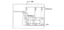
前述したようなアモルファスシリコンフォトダイオードで構成した光センサー装置には以下のような課題があった。アモルファスシリコンフォトダイオードは前述したように光感度が人間の視覚感度に近いと言う長所がある反面、その出力電流が単結晶シリコンフォトダイオードに比べて小さいという問題があった。したがって、アモルファスシリコンフォトダイオードでは、直接ほかの回路を動かすことが困難であり、図5に示すようにアモルファスフォトダイオード502と外部増幅回路501、帰還抵抗503とを組み合わせて、光センサー装置を構成し、アモルファスフォトダイオード502の出力電流を帰還抵抗503で電圧に変換し、出力端子504から電圧出力として、取り出していた。
前述したような従来の光センサー装置では、アモルファスフォトダイオード502と外部増幅回路501、帰還抵抗503とを組み合わせていたため、コストが高い、実装面積が大きいなどの問題点があった。また、アモルファスフォトダイオード502の出力がプリント基板上において、外部増幅回路501と接続されているため、ノイズが重畳しやすいなどの問題点があった。 In the conventional optical sensor device as described above, since the amorphous photodiode 502, the external amplifier circuit 501, and the feedback resistor 503 are combined, there are problems such as high cost and large mounting area. Further, since the output of the amorphous photodiode 502 is connected to the external amplifier circuit 501 on the printed circuit board, there is a problem that noise is easily superimposed.
以上のような問題を解決するため、本発明者らは光センサー素子と薄膜トランジスタによる増幅回路を一体形成することを考えた。アモルファスシリコンを用いた光センサー素子(アモルファスシリコンフォトダイオードなど)は通常絶縁基板上に形成される。同様に薄膜トランジスタもまた通常絶縁基板上に形成されるのであるから、両者は共通点が多い。本発明の光センサー装置は光センサー素子と薄膜トランジスタ(以下TFT)で構成した増幅回路を基板上に一体形成することによって、コストを低減し、実装面積を削減することを可能としている。また、光センサー素子と増幅回路が直接、センサー基板上で接続されているため、ノイズが重畳しにくいという特徴を有している。
また、アモルファスシリコンのみでなく、ポリシリコンを用いたセンサー素子、たとえばポリシリコンフォトダイオードなどにも本発明は適応できる。
In order to solve the above problems, the present inventors considered to integrally form an optical sensor element and an amplifier circuit using a thin film transistor. An optical sensor element using amorphous silicon (such as an amorphous silicon photodiode) is usually formed on an insulating substrate. Similarly, since a thin film transistor is usually formed on an insulating substrate, both have many common points. In the optical sensor device of the present invention, an amplifier circuit composed of an optical sensor element and a thin film transistor (hereinafter referred to as TFT) is integrally formed on a substrate, whereby the cost and the mounting area can be reduced. Further, since the optical sensor element and the amplifier circuit are directly connected on the sensor substrate, noise is hardly superimposed.
Further, the present invention can be applied not only to amorphous silicon but also to a sensor element using polysilicon, such as a polysilicon photodiode.
以下に本発明の構成を示す。 The configuration of the present invention is shown below.
本発明は光センサー素子と増幅回路を有する光センサー装置において、前記光センサー素子と前記増幅回路は基板上に一体形成されていることを特徴としている。 The present invention is an optical sensor device having an optical sensor element and an amplifier circuit, wherein the optical sensor element and the amplifier circuit are integrally formed on a substrate.
本発明は上記において、光センサー素子はアモルファスシリコンを用いたセンサー素子によって構成されていることを特徴としている。 In the above, the present invention is characterized in that the optical sensor element is constituted by a sensor element using amorphous silicon.
本発明は上記において、光センサー素子はアモルファスシリコンフォトダイオードによって構成されていることを特徴としている。 In the above, the present invention is characterized in that the optical sensor element is constituted by an amorphous silicon photodiode.
本発明は上記において、光センサー素子はポリシリコンを用いたセンサー素子によって構成されていることを特徴としている。 In the above, the present invention is characterized in that the optical sensor element is constituted by a sensor element using polysilicon.
本発明は上記において、光センサー素子はポリシリコンフォトダイオードによって構成されていることを特徴としている。 In the above, the present invention is characterized in that the optical sensor element is constituted by a polysilicon photodiode.
本発明は光センサー素子と増幅回路を有する光センサー装置において、前記増幅回路は薄膜トランジスタで構成され、前記光センサー素子と前記増幅回路は基板上に一体形成されていることを特徴としている。 The present invention is an optical sensor device having an optical sensor element and an amplifier circuit, wherein the amplifier circuit is composed of a thin film transistor, and the optical sensor element and the amplifier circuit are integrally formed on a substrate.
本発明は光センサー素子と増幅回路を有する光センサー装置において、前記増幅回路は薄膜トランジスタで構成された演算増幅器であり、前記光センサー素子と前記増幅回路は基板上に一体形成されていることを特徴としている。 The present invention is an optical sensor device having an optical sensor element and an amplifier circuit, wherein the amplifier circuit is an operational amplifier composed of a thin film transistor, and the optical sensor element and the amplifier circuit are integrally formed on a substrate. It is said.
本発明は光センサー素子と増幅回路と帰還抵抗を有する光センサー装置において、前記増幅回路は薄膜トランジスタで構成された演算増幅器であり、前記光センサー素子と前記増幅回路は基板上に一体形成され、前記帰還抵抗を前記基板外に有することを特徴としている。 The present invention relates to an optical sensor device having an optical sensor element, an amplifier circuit, and a feedback resistor, wherein the amplifier circuit is an operational amplifier composed of a thin film transistor, and the optical sensor element and the amplifier circuit are integrally formed on a substrate, A feedback resistor is provided outside the substrate.
本発明は光センサー素子と増幅回路とIV変換抵抗を有する光センサー装置において、前記増幅回路は薄膜トランジスタで構成された演算増幅器であり、前記光センサー素子と前記増幅回路は基板上に一体形成され、前記IV変換抵抗を前記基板外に有することを特徴としている。 The present invention is an optical sensor device having an optical sensor element, an amplifier circuit, and an IV conversion resistor, wherein the amplifier circuit is an operational amplifier composed of a thin film transistor, and the optical sensor element and the amplifier circuit are integrally formed on a substrate, The IV conversion resistor is provided outside the substrate.
本発明は光センサー素子と増幅回路とレベルシフト回路を有する光センサー装置において、前記増幅回路と前記レベルシフト回路は薄膜トランジスタで構成され、前記光センサー素子と前記増幅回路と前記レベルシフト回路は基板上に一体形成されることを特徴としている。 The present invention provides an optical sensor device having an optical sensor element, an amplifier circuit, and a level shift circuit, wherein the amplifier circuit and the level shift circuit are formed of thin film transistors, and the optical sensor element, the amplifier circuit, and the level shift circuit are on a substrate. It is characterized in that it is integrally formed.
本発明は上記において、前記レベルシフト回路はPチャネル型TFTと定電流源によって構成されていることを特徴としている。 The present invention is characterized in that, in the above, the level shift circuit includes a P-channel TFT and a constant current source.
本発明は上記において、前記レベルシフト回路はNチャネル型TFTと定電流源によって構成されていることを特徴としている。 The present invention is characterized in that, in the above, the level shift circuit includes an N-channel TFT and a constant current source.
本発明は上記において、前記基板上の接続電極端子が4端子であることを特徴としている。 In the above, the present invention is characterized in that the connection electrode terminals on the substrate are four terminals.
本発明は上記において、前記基板上の接続電極端子が4端子であり、そのうちの2端子が電源端子であることを特徴としている。 The present invention is characterized in that, in the above, the connection electrode terminals on the substrate are four terminals, and two of them are power supply terminals.
本発明は光センサー素子と増幅回路を有する光センサー装置において、前記増幅回路は薄膜トランジスタで構成されたカレントミラー回路であり、前記光センサー素子と前記増幅回路は基板上に一体形成されていることを特徴としている。 The present invention relates to an optical sensor device having an optical sensor element and an amplifier circuit, wherein the amplifier circuit is a current mirror circuit composed of a thin film transistor, and the optical sensor element and the amplifier circuit are integrally formed on a substrate. It is a feature.
本発明は上記において、カレントミラー回路を構成するTFTのゲートが複数から成る、マルチゲート構造によって構成されることを特徴としている。 In the above, the present invention is characterized by a multi-gate structure in which a plurality of TFT gates constituting a current mirror circuit are formed.
本発明は上記において、カレントミラー回路がカスコード接続で構成されていることを特徴としている。 In the above, the present invention is characterized in that the current mirror circuit is configured by cascode connection.
本発明は上記において、カレントミラー回路がウィルソン型接続で構成されていることを特徴としている。 In the above, the present invention is characterized in that the current mirror circuit is configured by a Wilson connection.
本発明は上記において、カレントミラー回路が改良ウィルソン型接続で構成されていることを特徴としている。 In the above, the present invention is characterized in that the current mirror circuit is constituted by an improved Wilson connection.
本発明は上記において、カレントミラー回路を構成するTFTの数、ゲート長L、チャネル幅Wを任意に変更することで、増幅率を選択することができることを特徴としている。 The present invention is characterized in that, in the above, the amplification factor can be selected by arbitrarily changing the number of TFTs constituting the current mirror circuit, the gate length L, and the channel width W.
本発明は上記において、前記カレントミラー回路がNチャネル型TFTによって構成されていることを特徴としている。 The present invention is characterized in that, in the above, the current mirror circuit is composed of an N-channel TFT.
本発明は上記において、前記カレントミラー回路がPチャネル型TFTによって構成されていることを特徴としている。 The present invention is characterized in that, in the above, the current mirror circuit is constituted by a P-channel TFT.
本発明は上記において、前記基板上の接続電気電極が2端子であることを特徴としている。 In the above, the present invention is characterized in that the connecting electrical electrode on the substrate has two terminals.
本発明は上記において、
前記光センサー素子および前記増幅回路はプラスチック基板上に一体形成されていることを特徴としている。
The present invention is as described above.
The optical sensor element and the amplifier circuit are integrally formed on a plastic substrate.
本発明は上記において、
前記光センサー素子および前記増幅回路はガラス基板上に一体形成されていることを特徴としている。
The present invention is as described above.
The optical sensor element and the amplifier circuit are integrally formed on a glass substrate.
本発明は、上記の光センサー装置を備える電子機器である。 The present invention is an electronic device including the above-described optical sensor device.
前述したように、本発明の光センサー装置では、フォトダイオードと、TFTを用いて構成された増幅回路をセンサー基板上に一体形成することによって、コスト、実装面積を削減することができ、ノイズの重畳を低減することができる。 As described above, in the optical sensor device of the present invention, the amplifier and the amplification circuit configured using the photodiode and the TFT are integrally formed on the sensor substrate, so that the cost and the mounting area can be reduced. Superposition can be reduced.
本発明の実施の形態について、図面を用いて詳細に説明する。ただし、本発明は以下の説明に限定されず、本発明の趣旨及びその範囲から逸脱することなくその形態及び詳細を様々に変更し得ることは当業者であれば容易に理解される。従って、本発明は以下に示す実施の形態の記載内容に限定して解釈されるものではない。 Embodiments of the present invention will be described in detail with reference to the drawings. However, the present invention is not limited to the following description, and it is easily understood by those skilled in the art that modes and details can be variously changed without departing from the spirit and scope of the present invention. Therefore, the present invention should not be construed as being limited to the description of the embodiments below.
また、本発明の実施の形態において、フォトダイオードに逆電圧(逆バイアスともいう)を印加して駆動する例を示す。このため、第2の電極から第1の電極へ電圧を印加する。また、第1の電極は、フォトダイオードのアモルファスシリコン層内のp層側に接する電極であり、第2の電極は、フォトダイオードのアモルファスシリコン層内のn層側に接する電極である。 In the embodiment of the present invention, an example in which a reverse voltage (also referred to as reverse bias) is applied to a photodiode and driven is shown. Therefore, a voltage is applied from the second electrode to the first electrode. Further, the first electrode is an electrode in contact with the p layer side in the amorphous silicon layer of the photodiode, and the second electrode is an electrode in contact with the n layer side in the amorphous silicon layer of the photodiode.
(実施形態1)
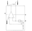
図1に本発明の第1の実施形態を示す。本実施形態はTFTで構成された増幅回路101、フォトダイオード102をセンサー基板上に一体形成している。以下その動作について説明をおこなう。増幅回路101の非反転入力端子は外部電源VBBに接続されている。外部電源VBBは増幅回路101の高電位側電源VDDと低電位側電源VSSの間の電位を有している。フォトダイオード102の第1の電極は外部電源VBBに接続され、第2の電極は増幅回路101の反転入力端子、および帰還抵抗103の第1の端子に接続されている。また、帰還抵抗103の第2の端子は増幅回路101の出力端子104に接続されている。ここで、帰還抵抗103は増幅回路101の出力電圧のばらつきを低減するため、センサー基板上には形成していないが、ばらつきがあまり問題にならない場合には帰還抵抗103をセンサー基板上に形成することも可能である。
(Embodiment 1)
FIG. 1 shows a first embodiment of the present invention. In this embodiment, an amplifier circuit 101 and a photodiode 102 made of TFTs are integrally formed on a sensor substrate. The operation will be described below. The non-inverting input terminal of the amplifier circuit 101 is connected to the external power supply VBB. The external power source VBB has a potential between the high potential side power source VDD and the low potential side power source VSS of the amplifier circuit 101. The first electrode of the photodiode 102 is connected to the external power supply VBB, and the second electrode is connected to the inverting input terminal of the amplifier circuit 101 and the first terminal of the feedback resistor 103. The second terminal of the feedback resistor 103 is connected to the output terminal 104 of the amplifier circuit 101. Here, the feedback resistor 103 is not formed on the sensor substrate in order to reduce variation in the output voltage of the amplifier circuit 101. However, if the variation is not a problem, the feedback resistor 103 is formed on the sensor substrate. It is also possible.
フォトダイオード102に光が入力されると、フォトダイオード102の第2の電極から第1の電極に光電流が流れる。これによって、増幅回路101の出力端子104から帰還抵抗103に電流が流れ、帰還抵抗103の両端に電圧が発生する。
本実施形態では増幅回路101の駆動能力を大きく取ることが可能であるため、出力端子104に負荷を接続し、駆動することが可能となる。
When light is input to the photodiode 102, a photocurrent flows from the second electrode of the photodiode 102 to the first electrode. As a result, a current flows from the output terminal 104 of the amplifier circuit 101 to the feedback resistor 103, and a voltage is generated across the feedback resistor 103.
In this embodiment, since the driving capability of the amplifier circuit 101 can be increased, a load can be connected to the output terminal 104 and driven.
また、フォトダイオードの向きを図1に示すものと逆に接続したものを図7に示す。図7の光センサー回路は増幅回路701、フォトダイオード702、帰還抵抗703によって構成され、フォトダイオード702の第1の電極が増幅回路701の反転入力端子と帰還抵抗703に接続され、第2の電極が外部電源VBBと増幅回路701の非反転入力端子に接続される。そして、電流は外部電源VBBからフォトダイオード702、帰還抵抗703を介して、増幅回路701の出力端子704に流れる。このようにフォトダイオードの向きはどちらも可能である。
本実施形態では、増幅回路101、701を演算増幅器(オペアンプ)として説明をおこなっているが、増幅回路101、701は演算増幅器には限定されない。
また、フォトダイオードに限らず他の光センサー素子でもよい。
FIG. 7 shows the photodiode connected in the reverse direction to that shown in FIG. 7 includes an amplifier circuit 701, a photodiode 702, and a feedback resistor 703. The first electrode of the photodiode 702 is connected to the inverting input terminal of the amplifier circuit 701 and the feedback resistor 703, and the second electrode. Are connected to the external power supply VBB and the non-inverting input terminal of the amplifier circuit 701. The current flows from the external power supply VBB to the output terminal 704 of the amplifier circuit 701 through the photodiode 702 and the feedback resistor 703. Thus, both directions of the photodiode are possible.
In the present embodiment, the amplifier circuits 101 and 701 are described as operational amplifiers (op-amps), but the amplifier circuits 101 and 701 are not limited to operational amplifiers.
Further, the photosensor element is not limited to the photodiode.
(実施形態2)
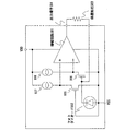
図2に本発明の第2の実施形態を示す。本実施形態はTFTで構成された増幅回路201、フォトダイオード202をセンサー基板上に一体形成している。以下その動作について説明をおこなう。増幅回路201の非反転入力端子はIV変換抵抗203の第1の端子とフォトダイオード202の第2の電極に接続されている。また増幅回路201の出力端子204は反転入力端子に接続され、増幅回路201はボルテージフォロワとして機能する。また、フォトダイオード202の第1の電極は外部電源VBB2に接続されている。IV変換抵抗203の第2の端子は外部電源VBB1に接続されている。ここで、IV変換抵抗203は出力電圧のばらつきを低減するため、センサー基板上には形成していないが、ばらつきがあまり問題にならない場合にはIV変換抵抗203をセンサー基板上に形成することも可能である。
(Embodiment 2)
FIG. 2 shows a second embodiment of the present invention. In the present embodiment, an amplifier circuit 201 and a photodiode 202 composed of TFTs are integrally formed on a sensor substrate. The operation will be described below. The non-inverting input terminal of the amplifier circuit 201 is connected to the first terminal of the IV conversion resistor 203 and the second electrode of the photodiode 202. The output terminal 204 of the amplifier circuit 201 is connected to the inverting input terminal, and the amplifier circuit 201 functions as a voltage follower. The first electrode of the photodiode 202 is connected to the external power supply VBB2. The second terminal of the IV conversion resistor 203 is connected to the external power supply VBB1. Here, the IV conversion resistor 203 is not formed on the sensor substrate in order to reduce variations in output voltage. However, if the variation is not a problem, the IV conversion resistor 203 may be formed on the sensor substrate. Is possible.
フォトダイオード202に光が入力されると、外部電源VBB1より、IV変換抵抗203を介して、フォトダイオード202の第2の電極から第1の電極に光電流が流れる。これによって、IV変換抵抗203の両端に電圧が発生する。
すなわち、光が入力されずフォトダイオード202に電流が流れない場合には、出力端子204にはVBB1と同じ電位が出力され、光が入力されフォトダイオード202に電流が流れるとその電流量に比例して、出力端子204の電位は低下する。
本実施形態では増幅回路201の駆動能力を大きく取ることが可能であるため、出力端子204に負荷を接続し、駆動することが可能となる。
When light is input to the photodiode 202, a photocurrent flows from the second electrode of the photodiode 202 to the first electrode via the IV conversion resistor 203 from the external power supply VBB1. As a result, a voltage is generated across the IV conversion resistor 203.
That is, when light is not input and current does not flow to the photodiode 202, the same potential as VBB1 is output to the output terminal 204, and when light is input and current flows to the photodiode 202, it is proportional to the amount of current. As a result, the potential of the output terminal 204 decreases.
In this embodiment, since the driving capability of the amplifier circuit 201 can be increased, a load can be connected to the output terminal 204 and driven.
また、フォトダイオードの向きを図2に示すものと逆に接続したものを図8に示す。図8の光センサー回路は増幅回路801、フォトダイオード802、IV変換抵抗803によって構成され、フォトダイオード802の第1の電極が増幅回路801の非反転入力端子とIV変換抵抗803に接続され、第2の電極が外部電源VBB2に接続される。そして、電流は外部電源VBB2からフォトダイオード802、IV変換抵抗803を介して、外部電源VBB1に流れる。このようにフォトダイオードの向きはどちらも可能である。
本実施形態では、増幅回路201、801を演算増幅器(オペアンプ)として説明をおこなっているが、増幅回路201、801は演算増幅器には限定されない。
また、フォトダイオードに限らず他の光センサー素子でもよい。
FIG. 8 shows the photodiode connected in the reverse direction to that shown in FIG. 8 includes an amplifier circuit 801, a photodiode 802, and an IV conversion resistor 803. The first electrode of the photodiode 802 is connected to the non-inverting input terminal of the amplifier circuit 801 and the IV conversion resistor 803, and Two electrodes are connected to the external power supply VBB2. The current flows from the external power supply VBB2 to the external power supply VBB1 via the photodiode 802 and the IV conversion resistor 803. Thus, both directions of the photodiode are possible.
In the present embodiment, the amplifier circuits 201 and 801 are described as operational amplifiers (op-amps), but the amplifier circuits 201 and 801 are not limited to operational amplifiers.
In addition, other photosensor elements are not limited to photodiodes.
(実施形態3)
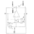
図3に本発明の第3の実施形態を示す。本実施形態はTFTで構成された増幅回路301、フォトダイオード302、レベルシフト回路305、306をセンサー基板上に一体形成している。以下その動作について説明をおこなう。レベルシフト回路305の入力は低電位側電源VSSに接続され、その出力は増幅回路301の非反転入力端子に接続されている。レベルシフト回路306の入力はフォトダイオード302の第2の電極および帰還抵抗303の第1の端子に接続され、その出力は増幅回路301の反転入力端子に接続されている。また、帰還抵抗303の第2の端子は増幅回路301の出力端子304に接続されている。フォトダイオード302の第1の電極は低電位側電源VSSに接続される。ここで、帰還抵抗303は増幅回路301の出力電圧のばらつきを低減するため、センサー基板上には形成していないが、ばらつきがあまり問題にならない場合には帰還抵抗303をセンサー基板上に形成することも可能である。
(Embodiment 3)
FIG. 3 shows a third embodiment of the present invention. In the present embodiment, an amplifier circuit 301, a photodiode 302, and
フォトダイオード302に光が入力されると、フォトダイオード302の第2の電極から第1の電極に光電流が流れる。これによって、増幅回路301の出力端子から帰還抵抗303に電流が流れ、帰還抵抗303の両端に電圧が発生する。
本実施形態では増幅回路301の駆動能力を大きく取ることが可能であるため、出力端子304に負荷を接続し、駆動することが可能となる。
When light is input to the photodiode 302, a photocurrent flows from the second electrode of the photodiode 302 to the first electrode. As a result, a current flows from the output terminal of the amplifier circuit 301 to the feedback resistor 303, and a voltage is generated across the feedback resistor 303.
In the present embodiment, since the driving capability of the amplifier circuit 301 can be increased, a load can be connected to the output terminal 304 and driven.
このようなレベルシフト回路を用いることの利点は以下のようなものがある。一体型センサーチップ600の外形図を図6に示す。図6(A)に示すように、チップ600の上面にはフォトダイオード部601と増幅回路部602が形成される。また図6(B)の側面図、図6(C)の下面図に示すように、チップの基板603およびTFT形成領域604の下面には接続電極端子605が形成される。このようなセンサーチップではチップ上の4点で接続電極端子を構成し、プリント基板などの上に実装をおこなうのが、強度的に望ましい。ところが前述した第1の実施形態では端子の数が5端子となるため、これを満たさない。
The advantages of using such a level shift circuit are as follows. An outline view of the integrated sensor chip 600 is shown in FIG. As shown in FIG. 6A, a photodiode portion 601 and an
また、第1の実施形態では、高電位側電源VDD、低電位側電源VSSのほかにVBBという電源が必要となる。よって、レベルシフタを用いることによって、図3に示すように電源数を削減することが可能となる。
本実施形態では、増幅回路301を演算増幅器(オペアンプ)として説明をおこなっているが、増幅回路301は演算増幅器には限定されない。
また、フォトダイオードに限らず他の光センサー素子でもよい。
In the first embodiment, a power source VBB is required in addition to the high potential side power source VDD and the low potential side power source VSS. Therefore, by using the level shifter, the number of power supplies can be reduced as shown in FIG.
In the present embodiment, the amplifier circuit 301 is described as an operational amplifier (op-amp), but the amplifier circuit 301 is not limited to an operational amplifier.
In addition, other photosensor elements are not limited to photodiodes.
(実施形態4)
図4に本発明の第4の実施形態を示す。本実施形態はTFTで構成された増幅回路401、フォトダイオード402、レベルシフト回路405、406をセンサー基板上に一体形成している。以下その動作について説明をおこなう。レベルシフト回路405の入力はIV変換抵抗403の第1の端子とフォトダイオード402の第2の電極に接続され、その出力は増幅回路401の非反転入力端子に接続されている。レベルシフト回路406の入力は出力端子404に接続され、その出力は増幅回路401の反転入力端子に接続されている、そして増幅回路401はボルテージフォロワとして機能する。また、フォトダイオード402の第1の電極は増幅回路401の低電位側電源VSSに接続されている。IV変換抵抗403の第2の端子は外部電源VBBに接続されている。ここで、IV変換抵抗403は出力電圧のばらつきを低減するため、センサー基板上には形成していないが、ばらつきがあまり問題にならない場合にはIV変換抵抗403をセンサー基板上に形成することも可能である。
(Embodiment 4)
FIG. 4 shows a fourth embodiment of the present invention. In the present embodiment, an amplifier circuit 401, a photodiode 402, and
フォトダイオード402に光が入力されると、フォトダイオード402の第2の電極から第1の電極に光電流が流れる。これによって、IV変換抵抗403に電流が流れ、IV変換抵抗403の両端に電圧が発生する。
すなわち、光が入力されずフォトダイオード402に電流が流れない場合には、出力端子404にはVBBと同じ電位が出力され、光が入力されフォトダイオード402に電流が流れるとその電流量に比例して、出力端子404の電位は低下する。
本実施形態では増幅回路401の駆動能力を大きく取ることが可能であるため、出力端子404に負荷を接続し、駆動することが可能となる。
When light is input to the photodiode 402, a photocurrent flows from the second electrode of the photodiode 402 to the first electrode. As a result, a current flows through the IV conversion resistor 403, and a voltage is generated across the IV conversion resistor 403.
That is, when light is not input and current does not flow to the photodiode 402, the same potential as VBB is output to the output terminal 404, and when light is input and current flows to the photodiode 402, it is proportional to the amount of current. As a result, the potential of the output terminal 404 decreases.
In this embodiment, since the driving capability of the amplifier circuit 401 can be increased, a load can be connected to the output terminal 404 and driven.
このようなレベルシフト回路を用いることの利点は以下のようなものがある。一体型センサーチップの外形図を図6に示す。図6(A)に示すように、チップの上面にはフォトダイオード部601と増幅回路部602が形成される。また図6(B)の側面図、図6(C)の下面図に示すように、チップの下面には接続電極605が形成される。このようなセンサーチップではチップ上の4点で接続電極端子を構成し、プリント基板などの上に実装をおこなうのが、強度的に望ましい。ところが前述した第2の実施形態では端子の数が5端子となるため、これを満たさない。
The advantages of using such a level shift circuit are as follows. An outline view of the integrated sensor chip is shown in FIG. As shown in FIG. 6A, a photodiode portion 601 and an
また、第2の実施形態では、高電位側電源VDD、低電位側電源VSS、外部電源VBB1のほかにVBB2という電源が必要となる。よって、レベルシフタを用いることによって、図4に示すように電源数を削減することが可能となる。
本実施形態では、増幅回路401を演算増幅器(オペアンプ)として説明をおこなっているが、増幅回路401は演算増幅器には限定されない。
また、フォトダイオードに限らず他の光センサー素子でもよい。
In the second embodiment, a power source VBB2 is required in addition to the high potential side power source VDD, the low potential side power source VSS, and the external power source VBB1. Therefore, by using the level shifter, the number of power supplies can be reduced as shown in FIG.
In the present embodiment, the amplifier circuit 401 is described as an operational amplifier (op-amp), but the amplifier circuit 401 is not limited to an operational amplifier.
In addition, other photosensor elements are not limited to photodiodes.
(実施形態5)
図19に本発明の第5の実施形態を示す。本実施形態は、TFTで構成された増幅回路1901、フォトダイオード1902をセンサー基板上に一体形成している。以下その動作について説明をおこなう。増幅回路1901のTFTのソース領域は外部電源GNDに接続され、Y側TFTのドレイン領域は出力端子1904に接続されている。増幅回路1901のX側TFTドレイン領域はフォトダイオード1902の第1の電極と接続、第2の電極は出力端子1904と接続されている。
(Embodiment 5)
FIG. 19 shows a fifth embodiment of the present invention. In this embodiment, an amplifier circuit 1901 and a photodiode 1902 made of TFTs are integrally formed on a sensor substrate. The operation will be described below. The source region of the TFT of the amplifier circuit 1901 is connected to the external power supply GND, and the drain region of the Y side TFT is connected to the output terminal 1904. The X-side TFT drain region of the amplifier circuit 1901 is connected to the first electrode of the photodiode 1902, and the second electrode is connected to the output terminal 1904.
フォトダイオード1902に光が入力されると、フォトダイオード1902の第2の電極から第1の電極に光電流が流れる。これによって、増幅回路1901のX側TFTに電流が流れ、その電流を流すのに必要な電圧がゲートに発生する。
Y側TFTの並列接続数、ゲート長L、チャネル幅WがX側TFTと等しければ、飽和領域において、TFTX側、Y側両方のゲート電圧が等しいため同じ電流が流れる。所望の増幅を得るには、例えば”X側TFT数:Y側TFT数 = 1:n”とすればn倍となる(ただし、他のX側、Y側の特性は同じものとする)。
When light is input to the photodiode 1902, a photocurrent flows from the second electrode of the photodiode 1902 to the first electrode. As a result, a current flows through the X-side TFT of the amplifier circuit 1901, and a voltage necessary to flow the current is generated at the gate.
If the number of Y-side TFTs connected in parallel, the gate length L, and the channel width W are equal to the X-side TFT, the same current flows in the saturation region because the gate voltages on both the TFT X-side and Y-side are equal. In order to obtain a desired amplification, for example, if “the number of TFTs on the X side: the number of TFTs on the Y side = 1: n”, the multiplication becomes n times (however, the other X side and Y side characteristics are the same).
また、図19(A)に示した回路に実装されるTFTはNチャネル型TFTであるが、Pチャネル型TFTを用いたものを図19(B)に示す。図19(B)の光センサー回路は増幅回路1901、フォトダイオード1902によって構成され、増幅回路1901のY側TFTのドレイン領域は外部電源GNDに接続され、ソース領域は出力端子1904に接続されている。増幅回路1901のX側TFTのドレイン領域はフォトダイオード1902の第2の電極と接続し、フォトダイオード1902の第1の電極はGNDと接続されている。本実施形態では、フォトダイオードに限らず他の光センサー素子でもよい。 The TFT mounted on the circuit shown in FIG. 19A is an N-channel TFT, but a TFT using a P-channel TFT is shown in FIG. 19B. The photosensor circuit in FIG. 19B includes an amplifier circuit 1901 and a photodiode 1902. The drain region of the Y-side TFT of the amplifier circuit 1901 is connected to the external power supply GND, and the source region is connected to the output terminal 1904. . The drain region of the X-side TFT of the amplifier circuit 1901 is connected to the second electrode of the photodiode 1902, and the first electrode of the photodiode 1902 is connected to GND. In this embodiment, not only a photodiode but another optical sensor element may be used.
(実施形態6)
図20に本発明の第6の実施形態を示す。本実施形態は、TFTで構成された増幅回路2001、フォトダイオード2002をセンサー基板上に一体形成している。以下その動作について説明をおこなう。増幅回路2001内のTFTはX側、Y側両側とも直列に配置されソース領域とドレイン領域が接続され、そのゲートは共通接続され、マルチゲート構造となっている。そして、低電圧側の段のソース領域は外部電源GNDに接続され、Y側TFT高電圧側の段のドレイン領域は出力端子2004に接続されている。増幅回路2001のX側TFT高電圧側段のドレイン領域はフォトダイオード2002の第1の電極と接続、第2の電極は出力端子2004と接続されている。
(Embodiment 6)
FIG. 20 shows a sixth embodiment of the present invention. In the present embodiment, an amplifier circuit 2001 and a photodiode 2002 composed of TFTs are integrally formed on a sensor substrate. The operation will be described below. The TFTs in the amplifier circuit 2001 are arranged in series on both the X side and the Y side, the source region and the drain region are connected, and the gates are connected in common to form a multi-gate structure. The source region of the low voltage side stage is connected to the external power supply GND, and the drain region of the Y side TFT high voltage side is connected to the output terminal 2004. The drain region of the X-side TFT high voltage side of the amplifier circuit 2001 is connected to the first electrode of the photodiode 2002, and the second electrode is connected to the output terminal 2004.
フォトダイオード2002に光が入力されると、フォトダイオード2002の第2の電極から第1の電極に光電流が流れる。これによって、増幅回路2001のX側TFTに電流が流れ、その電流を流すのに必要な電圧がゲートに発生する。
X側、Y側両方のTFTにかかるゲート電圧が等しいので、Y側TFTの並列接続数、ゲート長L、チャネル幅WがX側TFTと等しければ、飽和領域において、同じ電流が流れる。所望の増幅を得るには、例えば”X側TFT並列接続数:Y側TFT並列接続数 = 1:n”とすればn倍となる(ただし、他のX側、Y側の特性は同じものとする)。
本実施形態では、増幅回路2001内のTFTの直列接続は二段として説明をおこなっているが、その段数には限定されない。また、各段のTFTの特性は同じ必要はないが、対応するX側とY側の関係は各段で同じ必要がある。
When light is input to the photodiode 2002, a photocurrent flows from the second electrode of the photodiode 2002 to the first electrode. As a result, a current flows through the X-side TFT of the amplifier circuit 2001, and a voltage necessary to flow the current is generated at the gate.
Since the gate voltages applied to both the X-side and Y-side TFTs are equal, the same current flows in the saturation region if the number of Y-side TFTs connected in parallel, the gate length L, and the channel width W are equal to those of the X-side TFT. To obtain the desired amplification, for example, if “X side TFT parallel connection number: Y side TFT parallel connection number = 1: n”, it becomes n times (however, the other X side and Y side characteristics are the same) And).
In this embodiment, the series connection of TFTs in the amplifier circuit 2001 is described as two stages, but the number of stages is not limited. The characteristics of the TFTs at each stage need not be the same, but the corresponding relationship between the X side and the Y side needs to be the same at each stage.
図20(A)に示した回路に実装されるTFTはNチャネル型TFTであり、図20(B)に示した回路はPチャネル型TFTである。本実施形態では、フォトダイオードに限らず他の光センサー素子でもよい。 The TFT mounted on the circuit shown in FIG. 20A is an N-channel TFT, and the circuit shown in FIG. 20B is a P-channel TFT. In this embodiment, not only a photodiode but another optical sensor element may be used.
(実施形態7)
図21に本発明の第7の実施形態を示す。本実施形態は、TFTで構成された増幅回路2101、フォトダイオード2102をセンサー基板上に一体形成している。以下その動作について説明をおこなう。増幅回路2101内のTFTはX側、Y側両側とも直列に配置されソース領域とドレイン領域が接続され、そのゲートの接続はX側TFTはダイオード接続で、それぞれが直列に接続された構造、Y側TFTは向かいのX側TFTのゲートと接続されている。そして、低電圧側の段のソース領域は外部電源GNDに接続され、Y側TFT高電圧側の段のドレイン領域は出力端子2104に接続されている。増幅回路2101のX側TFT高電圧側段のドレイン領域はフォトダイオード2102の第1の電極と接続、第2の電極は出力端子2104と接続されている。
(Embodiment 7)
FIG. 21 shows a seventh embodiment of the present invention. In this embodiment, an amplifier circuit 2101 and a photodiode 2102 made of TFTs are integrally formed on a sensor substrate. The operation will be described below. The TFT in the amplifier circuit 2101 is arranged in series on both sides of the X side and the Y side, the source region and the drain region are connected, and the gate connection is the diode side connection of the X side TFT, each of which is connected in series, Y The side TFT is connected to the gate of the opposite X side TFT. The source region of the low voltage side stage is connected to the external power supply GND, and the drain region of the Y side TFT high voltage side is connected to the output terminal 2104. The drain region of the X-side TFT high voltage side of the amplifier circuit 2101 is connected to the first electrode of the photodiode 2102, and the second electrode is connected to the output terminal 2104.
フォトダイオード2102に光が入力されると、フォトダイオード2102の第2の電極から第1の電極に光電流が流れる。これによって、増幅回路2101のX側TFTに電流が流れ、その電流を流すのに必要な電圧が各ゲートに発生する。
X側、Y側両方のTFTにかかるゲート電圧は対応する各段で等しいのため、Y側TFTの並列接続数、ゲート長L、チャネル幅WがX側TFTと等しければ、飽和領域において、同じ電流が流れる。所望の増幅を得るには、例えば”X側TFT並列接続数:Y側TFT並列接続数 = 1:n”とすればn倍となる(ただし、他のX側、Y側の特性は同じものとする)。
本実施形態では、増幅回路2101内のTFTの直列接続は二段として説明をおこなっているが、その段数には限定されない。また、各段のTFTの特性は同じ必要はないが、対応するX側とY側の関係は各段で同じ必要がある。
When light is input to the photodiode 2102, a photocurrent flows from the second electrode of the photodiode 2102 to the first electrode. As a result, a current flows through the X-side TFT of the amplifier circuit 2101, and a voltage necessary to flow the current is generated at each gate.
Since the gate voltage applied to both the X-side and Y-side TFTs is the same in each corresponding stage, if the number of Y-side TFTs connected in parallel, the gate length L, and the channel width W are equal to the X-side TFT, the same in the saturation region Current flows. To obtain the desired amplification, for example, if “X side TFT parallel connection number: Y side TFT parallel connection number = 1: n”, it becomes n times (however, the other X side and Y side characteristics are the same) And).
In the present embodiment, the series connection of TFTs in the amplifier circuit 2101 is described as two stages, but the number of stages is not limited. The characteristics of the TFTs at each stage need not be the same, but the corresponding relationship between the X side and the Y side needs to be the same at each stage.
図21(A)に示した回路に実装されるTFTはNチャネル型TFTであり、図21(B)に示した回路はPチャネル型TFTである。本実施形態では、フォトダイオードに限らず他の光センサー素子でもよい。 The TFT mounted on the circuit shown in FIG. 21A is an N-channel TFT, and the circuit shown in FIG. 21B is a P-channel TFT. In this embodiment, not only a photodiode but another optical sensor element may be used.
(実施形態8)
図22に本発明の第8の実施形態を示す。本実施形態は、TFTで構成された増幅回路2201、フォトダイオード2202をセンサー基板上に一体形成している。以下その動作について説明をおこなう。増幅回路2201内のTFTはウィルソン型カレントミラー回路接続で、低電圧側の段のソース領域は外部電源GNDに接続され、Y側TFTのドレイン領域は出力端子2204に接続されている。増幅回路2201のX側TFTドレイン領域はフォトダイオード2202の第1の電極と接続、第2の電極は出力端子2204と接続されている。
(Embodiment 8)
FIG. 22 shows an eighth embodiment of the present invention. In this embodiment, an amplifier circuit 2201 and a photodiode 2202 made of TFTs are integrally formed on a sensor substrate. The operation will be described below. The TFT in the amplifier circuit 2201 is connected by a Wilson current mirror circuit, the source region of the low voltage side stage is connected to the external power supply GND, and the drain region of the Y side TFT is connected to the output terminal 2204. The X-side TFT drain region of the amplifier circuit 2201 is connected to the first electrode of the photodiode 2202, and the second electrode is connected to the output terminal 2204.
フォトダイオード2202に光が入力されると、フォトダイオード2202の第2の電極から第1の電極に光電流が流れる。これによって、増幅回路2201のX側TFTに電流が流れ、その電流を流すのに必要な電圧が各ゲートに発生する。ウィルソン型カレントミラー回路は、Y側TFTの並列接続数、ゲート長L、チャネル幅WがX側TFTと等しければ、飽和領域において、同じ電流が流れる。所望の増幅を得るには、例えば”X側TFT並列接続数:Y側TFT並列接続数 = 1:n”とすればn倍となる(ただし、他のX側、Y側の特性は同じものとする)。
本実施形態では、増幅回路2201内のTFTの直列接続は二段として説明をおこなっているが、その段数には限定されない。また、各段のTFTの特性は同じ必要はないが、対応するX側とY側の関係は各段で同じ必要がある。
When light is input to the photodiode 2202, a photocurrent flows from the second electrode of the photodiode 2202 to the first electrode. As a result, a current flows through the X-side TFT of the amplifier circuit 2201, and a voltage required to flow the current is generated at each gate. In the Wilson current mirror circuit, if the number of Y-side TFTs connected in parallel, the gate length L, and the channel width W are equal to those of the X-side TFT, the same current flows in the saturation region. To obtain the desired amplification, for example, if “X side TFT parallel connection number: Y side TFT parallel connection number = 1: n”, it becomes n times (however, the other X side and Y side characteristics are the same) And).
In the present embodiment, the series connection of TFTs in the amplifier circuit 2201 is described as two stages, but the number of stages is not limited. The characteristics of the TFTs at each stage need not be the same, but the corresponding relationship between the X side and the Y side needs to be the same at each stage.
図22(A)に示した回路に実装されるTFTはNチャネル型TFTであり、図22(B)に示した回路はPチャネル型TFTである。本実施形態では、フォトダイオードに限らず他の光センサー素子でもよい。 The TFT mounted on the circuit shown in FIG. 22A is an N-channel TFT, and the circuit shown in FIG. 22B is a P-channel TFT. In this embodiment, not only a photodiode but another optical sensor element may be used.
(実施形態9)
図23に本発明の第9の実施形態を示す。本実施形態は、TFTで構成された増幅回路2301、フォトダイオード2302をセンサー基板上に一体形成している。以下その動作について説明をおこなう。増幅回路2301内のTFTは改良ウィルソン型カレントミラー回路接続である。図22に示したウィルソン型カレントミラー回路との違いは、X側とY側のTFTの数を同じにすることで、対応する各TFTにかかるソース−ドレイン間電圧を同じにし、このことによりTFTが有限の出力抵抗であっても、X側、Y側に両側に流れる電流が等しくなることである。上記、増幅回路2301の低電圧側の段のソース領域は外部電源GNDに接続され、Y側TFTのドレイン領域は出力端子2304に接続されている。増幅回路2301のX側TFTドレイン領域はフォトダイオード2302の第1の電極と接続、第2の電極は出力端子2304と接続されている。
(Embodiment 9)
FIG. 23 shows a ninth embodiment of the present invention. In the present embodiment, an amplifier circuit 2301 and a photodiode 2302 configured by TFTs are integrally formed on a sensor substrate. The operation will be described below. The TFT in the amplifier circuit 2301 has an improved Wilson current mirror circuit connection. The difference from the Wilson type current mirror circuit shown in FIG. 22 is that the number of TFTs on the X side and the Y side is made the same so that the source-drain voltages applied to the corresponding TFTs are made the same. Even if the output resistance is finite, the currents flowing on both sides of the X side and the Y side are equal. The source region of the low voltage side stage of the amplifier circuit 2301 is connected to the external power supply GND, and the drain region of the Y side TFT is connected to the output terminal 2304. The X-side TFT drain region of the amplifier circuit 2301 is connected to the first electrode of the photodiode 2302, and the second electrode is connected to the output terminal 2304.
フォトダイオード2302に光が入力されると、フォトダイオード2302の第2の電極から第1の電極に光電流が流れる。これによって、増幅回路2301のX側TFTに電流が流れ、その電流を流すのに必要な電圧が各ゲートに発生する。
X側、Y側両方のTFTにかかるゲート電圧は対応する各段で等しいため、Y側TFTの並列接続数、ゲート長L、チャネル幅WがX側TFTと等しければ、飽和領域において、同じ電流が流れる。所望の増幅を得るには、例えば”X側TFT並列接続数:Y側TFT並列接続数 = 1:n”とすればn倍となる(ただし、他のX側、Y側の特性は同じものとする)。
本実施形態では、増幅回路2301内のTFTの直列接続は二段として説明をおこなっているが、その段数には限定されない。また、各段のTFTの特性は同じ必要はないが、対応するX側とY側の関係は各段で同じ必要がある。
When light is input to the photodiode 2302, a photocurrent flows from the second electrode of the photodiode 2302 to the first electrode. As a result, a current flows through the X-side TFT of the amplifier circuit 2301, and a voltage necessary to flow the current is generated at each gate.
Since the gate voltage applied to both the X-side and Y-side TFTs is the same in each corresponding stage, if the number of Y-side TFTs connected in parallel, the gate length L, and the channel width W are equal to those of the X-side TFT, the same current in the saturation region Flows. To obtain the desired amplification, for example, if “X side TFT parallel connection number: Y side TFT parallel connection number = 1: n”, it becomes n times (however, the other X side and Y side characteristics are the same) And).
In this embodiment, the series connection of TFTs in the amplifier circuit 2301 is described as two stages, but the number of stages is not limited. The characteristics of the TFTs at each stage need not be the same, but the corresponding relationship between the X side and the Y side needs to be the same at each stage.
図23(A)に示した回路に実装されるTFTはNチャネル型TFTであり、図23(B)に示した回路はPチャネル型TFTである。本実施形態では、フォトダイオードに限らず他の光センサー素子でもよい。 The TFT mounted on the circuit shown in FIG. 23A is an N-channel TFT, and the circuit shown in FIG. 23B is a P-channel TFT. In this embodiment, not only a photodiode but another optical sensor element may be used.
図9に本発明の第1の実施例を示す。本実施例はレベルシフト回路を用いた実施形態3を具体化したものである。本実施例はTFTで構成された増幅回路901、フォトダイオード902、Pチャネル型TFT905、906、定電流源907、908によって構成された2組のレベルシフト回路をセンサー基板上に一体形成している。以下その動作について説明をおこなう。Pチャネル型TFT905、定電流源907によって構成されるレベルシフト回路の入力は低電位側電源VSSに接続され、その出力は増幅回路901の非反転入力端子に接続されている。Pチャネル型TFT906、定電流源908によって構成されるレベルシフト回路の入力はフォトダイオード902の第2の電極と帰還抵抗903の第1の端子に接続され、その出力は増幅回路901の反転入力端子に接続される。フォトダイオード902の第1の電極は低電位側電源VSSに接続される。また、帰還抵抗903の第2の端子は増幅回路901の出力端子904に接続されている。ここで、帰還抵抗903は増幅回路901の出力電圧のばらつきを低減するため、センサー基板上には形成していないが、ばらつきがあまり問題にならない場合には帰還抵抗903をセンサー基板上に形成することも可能である。
FIG. 9 shows a first embodiment of the present invention. This embodiment is a specific implementation of Embodiment 3 using a level shift circuit. In this embodiment, two sets of level shift circuits each composed of an amplifying circuit 901 composed of TFTs, a photodiode 902, P-
フォトダイオード902に光が入力されると、フォトダイオードの第2の電極902から第1の電極に光電流が流れる。これによって、増幅回路901の出力端子904から帰還抵抗903に電流が流れ、帰還抵抗903の両端に電圧が発生する。
本実施例では増幅回路901の駆動能力を大きく取ることが可能であるため、出力端子904に負荷を接続し、駆動することが可能となる。
本実施例では光センサー装置の接続電極端子を高電位側電源VDD、低電位側電源VSS、増幅回路901出力端子904、帰還抵抗903−フォトダイオード902接続端子の4端子にすることができ、前述した実装強度を向上させることができる。また、レベルシフタを用いることによって、電源数を2電源にすることが可能となる。
本実施例では、増幅回路901を演算増幅器(オペアンプ)として説明をおこなっているが、増幅回路901は演算増幅器には限定されない。
また、フォトダイオードに限らず他の光センサー素子でもよい。
When light is input to the photodiode 902, a photocurrent flows from the second electrode 902 of the photodiode to the first electrode. As a result, a current flows from the output terminal 904 of the amplifier circuit 901 to the feedback resistor 903, and a voltage is generated across the feedback resistor 903.
In this embodiment, since the driving capability of the amplifier circuit 901 can be increased, a load can be connected to the output terminal 904 for driving.
In this embodiment, the connection electrode terminals of the photosensor device can be made into four terminals of a high potential side power supply VDD, a low potential side power supply VSS, an amplifier circuit 901 output terminal 904, and a feedback resistor 903-photodiode 902 connection terminal. The mounting strength can be improved. Further, by using the level shifter, the number of power supplies can be two.
In this embodiment, the amplifier circuit 901 is described as an operational amplifier (op-amp), but the amplifier circuit 901 is not limited to an operational amplifier.
In addition, other photosensor elements are not limited to photodiodes.
図10に本発明の第2の実施例を示す。本実施例はレベルシフト回路を用いた実施形態3を具体化したものである。本実施例はTFTで構成された増幅回路1001、フォトダイオード1002、Nチャネル型TFT1005、1006、定電流源1007、1008によって構成された2組のレベルシフト回路をセンサー基板上に一体形成している。以下その動作について説明をおこなう。Nチャネル型TFT1005、定電流源1007によって構成されるレベルシフト回路の入力は高電位側電源VDDに接続され、その出力は増幅回路1001の非反転入力端子に接続されている。Nチャネル型TFT1006、定電流源1008によって構成されるレベルシフト回路の入力はフォトダイオード1002の第1の電極と帰還抵抗1003の第1の端子に接続され、その出力は増幅回路1001の反転入力端子に接続される。フォトダイオード1002の第2の電極は高電位側電源VDDに接続される。また、帰還抵抗1003の第2の端子は増幅回路1001の出力端子1004に接続されている。ここで、帰還抵抗1003は増幅回路1001の出力電圧のばらつきを低減するため、センサー基板上には形成していないが、ばらつきがあまり問題にならない場合には帰還抵抗1003をセンサー基板上に形成することも可能である。
FIG. 10 shows a second embodiment of the present invention. This embodiment is a specific implementation of Embodiment 3 using a level shift circuit. In this embodiment, two sets of level shift circuits each formed by an amplifier circuit 1001, a photodiode 1002, N-
フォトダイオード1002に光が入力されると、フォトダイオード1002の第2の電極から第1の電極に光電流が流れる。これによって、帰還抵抗1003を介して、増幅回路1001の出力端子1004に電流が流れ、帰還抵抗1003の両端に電圧が発生する。
本実施例では増幅回路1001の駆動能力を大きく取ることが可能であるため、出力端子1004に負荷を接続し、駆動することが可能となる。
本実施例では光センサー装置の接続電極端子を高電位側電源VDD、低電位側電源VSS、増幅回路1001出力端子1004、帰還抵抗1003−フォトダイオード1002接続端子の4端子にすることができ、前述した実装強度を向上させることができる。また、レベルシフタを用いることによって、電源数を2電源にすることが可能となる。
本実施例では、増幅回路1001を演算増幅器(オペアンプ)として説明をおこなっているが、増幅回路1001は演算増幅器には限定されない。
また、フォトダイオードに限らず他の光センサー素子でもよい。
When light is input to the photodiode 1002, a photocurrent flows from the second electrode of the photodiode 1002 to the first electrode. As a result, a current flows to the output terminal 1004 of the amplifier circuit 1001 via the feedback resistor 1003, and a voltage is generated across the feedback resistor 1003.
In this embodiment, since the driving capability of the amplifier circuit 1001 can be increased, a load can be connected to the output terminal 1004 for driving.
In this embodiment, the connection electrode terminals of the photosensor device can be made into four terminals of the high potential side power supply VDD, the low potential side power supply VSS, the amplifier circuit 1001 output terminal 1004 and the feedback resistor 1003 -photodiode 1002 connection terminal. The mounting strength can be improved. Further, by using the level shifter, the number of power supplies can be two.
In this embodiment, the amplifier circuit 1001 is described as an operational amplifier (op-amp), but the amplifier circuit 1001 is not limited to an operational amplifier.
In addition, other photosensor elements are not limited to photodiodes.
図11に本発明の第3の実施例を示す。本実施例は前述した実施形態4を具体化したものである。本実施例はTFTで構成された増幅回路1101、フォトダイオード1102、TFT1105、1106、定電流源1107、1108によって構成される2組のレベルシフト回路のセンサー基板上に一体形成している。以下その動作について説明をおこなう。Pチャネル型TFT1105と定電流源1107によって構成されるレベルシフト回路に入力は、フォトダイオード1102の第1の電極とIV変換抵抗1103の第1の端子に接続され、その出力は増幅回路1101の非反転入力端子に接続される。Pチャネル型TFT1106と定電流源1108によって構成されるレベルシフト回路の入力は増幅回路1101の出力端子1104に接続され、その出力は増幅回路1101の反転入力端子に接続される。ここで増幅回路1101はボルテージフォロワとして機能する。また、フォトダイオード1102の第2の電極は高電位側電源VDDに接続されている。IV変換抵抗1103の第2の端子は外部電源VBBに接続されている。ここで、IV変換抵抗1103は出力電圧のばらつきを低減するため、センサー基板上には形成していないが、ばらつきがあまり問題にならない場合にはIV変換抵抗1103をセンサー基板上に形成することも可能である。
FIG. 11 shows a third embodiment of the present invention. The present example is a specific example of the fourth embodiment described above. In this embodiment, an amplifier circuit 1101 composed of TFTs, a photodiode 1102,
フォトダイオード1102に光が入力されると、フォトダイオード1102の第2の電極から第1の電極に光電流が流れる。これによって、IV変換抵抗1103に電流が流れ、IV変換抵抗1103の両端に電圧が発生する。
すなわち、光が入力されずフォトダイオード1102に電流が流れない場合には、出力端子1104にはVBBと同じ電位が出力され、光が入力されフォトダイオード1102に電流が流れるとその電流量に比例して、出力端子1104の電位は上昇する。
本実施例では増幅回路1101の駆動能力を大きく取ることが可能であるため、出力端子1104に負荷を接続し、駆動することが可能となる。
本実施例では光センサー装置の接続電極端子を高電位側電源VDD、低電位側電源VSS、増幅回路1101出力端子1104、IV変換抵抗1103−フォトダイオード1102接続端子の4端子にすることができ、前述した実装強度を向上させることができる。また、レベルシフタを用いることによって、電源数を2電源にすることが可能となる。
本実施例では、増幅回路1101を演算増幅器(オペアンプ)として説明をおこなっているが、増幅回路1101は演算増幅器には限定されない。
また、フォトダイオードに限らず他の光センサー素子でもよい。
When light is input to the photodiode 1102, a photocurrent flows from the second electrode of the photodiode 1102 to the first electrode. As a result, a current flows through the IV conversion resistor 1103 and a voltage is generated across the IV conversion resistor 1103.
That is, when light is not input and current does not flow to the photodiode 1102, the same potential as VBB is output to the output terminal 1104. When light is input and current flows to the photodiode 1102, the current is proportional to the amount of current. Thus, the potential of the output terminal 1104 rises.
In this embodiment, since the driving capability of the amplifier circuit 1101 can be increased, a load can be connected to the output terminal 1104 for driving.
In this embodiment, the connection electrode terminals of the optical sensor device can be made into four terminals of a high potential side power source VDD, a low potential side power source VSS, an amplifier circuit 1101 output terminal 1104, an IV conversion resistor 1103 and a photodiode 1102 connection terminal, The mounting strength described above can be improved. Further, by using the level shifter, the number of power supplies can be two.
In this embodiment, the amplifier circuit 1101 is described as an operational amplifier (op-amp), but the amplifier circuit 1101 is not limited to an operational amplifier.
In addition, other photosensor elements are not limited to photodiodes.
図12に本発明の第4の実施例を示す。本実施例は前述した実施形態4を具体化したものである。本実施例はTFTで構成された増幅回路1201、フォトダイオード1202、TFT1205、1206、定電流源1207、1208によって構成される2組のレベルシフト回路をセンサー基板上に一体形成している。以下その動作について説明をおこなう。Nチャネル型TFT1205と定電流源1207によって構成されるレベルシフト回路の入力は、フォトダイオード1202の第2の電極とIV変換抵抗1203の第1の端子に接続され、その出力は増幅回路1201の非反転入力端子に接続される。Nチャネル型TFT1206と定電流源1208によって構成されるレベルシフト回路の入力は増幅回路1201の出力端子1204に接続され、その出力は増幅回路1201の反転入力端子に接続される。ここで増幅回路1201はボルテージフォロワとして機能する。また、フォトダイオード1202の第1の電極は低電位側電源VSSに接続されている。IV変換抵抗1203の第2の端子は外部電源VBBに接続されている。ここで、IV変換抵抗1203は出力電圧のばらつきを低減するため、センサー基板上には形成していないが、ばらつきがあまり問題にならない場合にはIV変換抵抗1203をセンサー基板上に形成することも可能である。
FIG. 12 shows a fourth embodiment of the present invention. The present example is a specific example of the fourth embodiment described above. In this embodiment, two sets of level shift circuits each including an amplifier circuit 1201, a photodiode 1202,
フォトダイオード1202に光が入力されると、フォトダイオード1202の第2の電極から第1の電極に光電流が流れる。これによって、IV変換抵抗1203に電流が流れ、IV変換抵抗1203の両端に電圧が発生する。
すなわち、光が入力されずフォトダイオード1202に電流が流れない場合には、出力端子1204にはVBBと同じ電位が出力され、光が入力されフォトダイオード1202に電流が流れるとその電流量に比例して、出力端子1204の電位は低下する。
本実施例では増幅回路1201の駆動能力を大きく取ることが可能であるため、出力端子1204に負荷を接続し、駆動することが可能となる。
本実施例では光センサー装置の接続電極端子を高電位側電源VDD、低電位側電源VSS、増幅回路1201出力端子1204、IV変換抵抗1203−フォトダイオード1202接続端子の4端子にすることができ、前述した実装強度を向上させることができる。また、レベルシフタを用いることによって、電源数を2電源にすることが可能となる。
本実施例では、増幅回路1201を演算増幅器(オペアンプ)として説明をおこなっているが、増幅回路1201は演算増幅器には限定されない。
また、フォトダイオードに限らず他の光センサー素子でもよい。
When light is input to the photodiode 1202, a photocurrent flows from the second electrode of the photodiode 1202 to the first electrode. As a result, a current flows through the IV conversion resistor 1203 and a voltage is generated across the IV conversion resistor 1203.
That is, when light is not input and current does not flow to the photodiode 1202, the same potential as VBB is output to the output terminal 1204. When light is input and current flows to the photodiode 1202, the current is proportional to the amount of current. Thus, the potential of the output terminal 1204 decreases.
In this embodiment, since the driving capability of the amplifier circuit 1201 can be increased, a load can be connected to the output terminal 1204 for driving.
In this embodiment, the connection electrode terminals of the optical sensor device can be made into four terminals of a high potential side power supply VDD, a low potential side power supply VSS, an amplifier circuit 1201 output terminal 1204, an IV conversion resistor 1203 and a photodiode 1202 connection terminal, The mounting strength described above can be improved. Further, by using the level shifter, the number of power supplies can be two.
In this embodiment, the amplifier circuit 1201 is described as an operational amplifier (op-amp), but the amplifier circuit 1201 is not limited to an operational amplifier.
In addition, other photosensor elements are not limited to photodiodes.
図14は薄膜半導体素子、特にTFTを用いて、増幅回路とくに演算増幅器(以下オペアンプ)回路を作成した場合の等価回路図である。このオペアンプは、TFT1401、TFT1402で構成される差動回路、TFT1403、TFT1404で構成されるカレントミラー回路、TFT1405、TFT1409で構成される定電流源、TFT1406で構成されるソース接地回路、TFT1407、TFT1408で構成されるアイドリング回路、TFT1410、TFT1411で構成されるソースフォロワ回路、位相補償コンデンサ1412より成り立っている。
FIG. 14 is an equivalent circuit diagram in the case where an amplifier circuit, particularly an operational amplifier (hereinafter referred to as operational amplifier) circuit, is formed using thin film semiconductor elements, particularly TFTs. This operational amplifier includes a differential circuit composed of
以下に、図14のオペアンプ回路の動作を説明する。非反転入力端子に+信号が入力されると、差動回路を構成するTFT1401、1402のソースにはTFT1405で構成される定電流源が接続されているため、TFT1401のドレイン電流がTFT1402のドレイン電流より大きくなり、TFT1403のドレイン電流は、TFT1404とTFT1403がカレントミラー回路を構成するため、TFT1402のドレイン電流と同じになり、TFT1403のドレイン電流とTFT1401のドレイン電流の差電流によって、TFT1406のゲート電位は低下する方向に変化する。TFT1406はPチャネル型TFTであるので、TFT1406のゲート電位が下がると、TFT1406はよりオンする方向に動作し、ドレイン電流が増加する。よって、TFT1410のゲート電位は上昇し、それに伴い、TFT1410のソース電位すなわち、出力端子の電位も上昇する。
The operation of the operational amplifier circuit shown in FIG. 14 will be described below. When a + signal is input to the non-inverting input terminal, a constant current source composed of the
また、非反転入力端子に−信号が入力されると、TFT1401のドレイン電流がTFT1402のドレイン電流より小さくなり、TFT1403のドレイン電流は、TFT1402のドレイン電流と同じであるため、TFT1403のドレイン電流とTFT1401のドレイン電流の差電流によって、TFT1406のゲート電位は上昇する方向に変化する。TFT1406はPチャネル型TFTであるので、TFT1406のゲート電位が上がると、TFT1406はオフする方向に動作し、ドレイン電流が減少する。よって、TFT1410のゲート電位は低下し、それに伴い、TFT1410のソース電位すなわち、出力端子の電位も低下する。このように非反転入力端子の信号と同相の信号が、出力端子より出力される。
When a negative signal is input to the non-inverting input terminal, the drain current of the
反転入力端子に+信号が入力されると、TFT1401のドレイン電流がTFT1402のドレイン電流より小さくなり、TFT1403のドレイン電流は、TFT1402のドレイン電流と同じであるため、TFT1403のドレイン電流とTFT1401の差電流によって、TFT1406のゲート電位は上昇する方向に変化する。TFT1406はPチャネル型TFTであるので、TFT1406のゲート電位が上がると、TFT1406はオフする方向に動作し、ドレイン電流が減少する。よって、TFT1410のゲート電位は低下し、それに伴い、TFT1410のソース電位すなわち、出力端子の電位も低下する。
When a + signal is input to the inverting input terminal, the drain current of the
また、反転入力端子に−信号が入力されると、TFT1401のドレイン電流がTFT1402のドレイン電流より大きくなり、TFT1403のドレイン電流は、TFT1402のドレイン電流と同じであるため、TFT1403のドレイン電流とTFT1401のドレイン電流の差電流によって、TFT1406のゲート電位は低下する方向に変化する。TFT1406はPチャネル型TFTであるので、TFT1406のゲート電位が下がると、TFT1406はよりオンする方向に動作し、ドレイン電流が増加する。よって、TFT1410のゲート電位は上昇し、それに伴い、TFT1410のソース電位すなわち、出力端子の電位も上昇する。このようにして、反転入力端子の信号と逆相の信号が出力端子より出力される。
When a negative signal is input to the inverting input terminal, the drain current of the
この例では、差動回路をNチャネル型TFT、カレントミラー回路をPチャネル型TFTで作成しているが、本発明では、それには限定されず逆であっても良い。また、回路形式もこのような回路形式には限定されることはなく、増幅回路としての機能を満たすものであれば使用可能である。
また、本実施例は前述した実施形態、実施例と組み合わせて使用することが可能である。
In this example, the differential circuit is made of an N-channel TFT and the current mirror circuit is made of a P-channel TFT. However, the present invention is not limited to this and may be reversed. Further, the circuit format is not limited to such a circuit format, and any circuit format that satisfies the function as an amplifier circuit can be used.
In addition, this example can be used in combination with the above-described embodiment and examples.
以下に本発明の光センサー装置の構造の一例について説明する。図17はフォトダイオードと増幅回路が一体形成されている光センサー装置を示しており、プリント基板等に実装する時に貼り付ける面方向から見た図である。 An example of the structure of the optical sensor device of the present invention will be described below. FIG. 17 shows an optical sensor device in which a photodiode and an amplifier circuit are integrally formed, and is a view seen from the direction of the surface to be attached when mounted on a printed circuit board or the like.
基板1701上に増幅回路1702及びフォトダイオード1703が形成され、その上部に接続電極端子1704が形成されている。接続電極端子1704はコンタクトホール1705を介して増幅回路1702及びフォトダイオード1703と接続されている。
An
増幅回路1702とフォトダイオード1703が接続されている部分1706の拡大図を線で示している。TFT1707はソース又はドレイン領域1708、1709及びチャネル形成領域(ここでは図示しない)及びソース又はドレイン電極1710、1711及びゲート電極1712で構成されている。
An enlarged view of a
ゲート電極1712上には層間絶縁膜(ここでは図示しない)が形成され、その上部の配線1713はコンタクトホール1714を介してゲート電極1712と接続されている。そして配線1713上にフォトダイオード1703の第1の電極1715が形成されている。
An interlayer insulating film (not shown here) is formed over the
次に、フォトダイオードと増幅回路が一体形成されている光センサー装置の断面図18(A)を用いて増幅回路1702のTFT1707とフォトダイオード1703が電気的に接続されている様子をより詳しく説明する。図18(A)は図17の線A−A’の断面図であり図17と共通する部分は共通の符号を用いている。基板1701上に接して下地絶縁膜1801が形成され、下地絶縁膜1801上にはTFT1707及びフォトダイオード1703が形成されている。
Next, a state in which the
半導体層1802はチャネル形成領域である。このチャネル形成領域の紙面表及び裏側にソース又はドレイン領域1708、1709が形成されている。半導体層1802上にはゲート絶縁膜1803を介してゲート電極1712が形成され、その上部に第1層間絶縁膜1804及び第2層間絶縁膜1805が形成されている。
The
TFT1707のゲート電極1712はコンタクトホール1714を介して配線1713によりフォトダイオード1703の第1の電極1715と接続されている。
A
フォトダイオード1703の第1の電極1715に接するようにP型半導体層1806が形成され、その上に光電変換層1807、N型半導体層1808が積層され、さらにNチャネル型半導体層1808上にフォトダイオード1703の第2の電極1809が形成されている。そしてフォトダイオード1703の第2の電極1809上には第3の層間絶縁膜1810が形成され、フォトダイオード1703の第2の電極1809はコンタクトホール1705を介して接続電極端子1704と接続されている。
A P-
フォトダイオード1703の第1の電極1715としてはITO(indium tin oxide)等のように透光性かつ導電性を有する物質を用いることで、フォトダイオード1703に入射する光を遮断しないようにすることができる。そしてフォトダイオード1703の第2の電極1809としては、Tiのように光を反射する物質を用いることでP型半導体層1806から入射した光のうち、光電変換層1807で光が吸収されずに光電変換層1807及びN型半導体層1808を通過した光を反射させることで、再び光電変換層1807で反射光を吸収させることができる。P型半導体層1806としてはP型の非晶質珪素膜(a−Si:H)又はいわゆるマイクロクリスタル半導体(μc−Si:H)、光電変換層1807としては非晶質珪素膜(a−Si:H)、N型半導体層1808としてはN型の非晶質珪素膜(a−Si:H)又はいわゆるマイクロクリスタル半導体(μc−Si:H)で形成することができる。
As the
図18(B)は図17の線B−B’の断面を線A−A’のA側から見た図であり、線B−B’の断面において、第3の層間絶縁膜1810を透かして見た時の様子を示している。
FIG. 18B is a view of the cross section taken along line BB ′ of FIG. 17 as viewed from the A side of line AA ′. In the cross section taken along line BB ′, the third
TFT1707は半導体層1802、ソース又はドレイン領域1708、1709、ソース又はドレイン電極1710、1711及びゲート電極1712からなり、ゲート電極1712が紙面裏側へ伸びコンタクトホール1714を介して配線1713によりフォトダイオード1703の第1の電極1715と接続されている。そしてフォトダイオード1703の第1の電極1715に接するようにPチャネル型半導体層1806が形成され、その上に光電変換層1807、Nチャネル型半導体層1808が積層され、さらにNチャネル型半導体層1808上にフォトダイオード1703の第2の電極1809が形成されている。そしてフォトダイオード1703の第2の電極1809上には第3の層間絶縁膜1810、接続電極端子1704が形成されている。接続電極端子1704はコンタクトホール(ここでは図示しない)を介してフォトダイオード1703の第2の電極1809と接続されている。
The
なお、本発明は実施例6で示した光センサー装置の構成に限定しているのではない。例えば増幅回路1702としてオペアンプの代わりにカレントミラー回路を備えた構成でも良い。また、光センサー素子も上記の構成に限られずポリシリコンフォトダイオードでも良く、フォトダイオードに限らず他の光センサー素子でもよい。
Note that the present invention is not limited to the configuration of the optical sensor device shown in the sixth embodiment. For example, the
図24(A)に本発明の第7の実施例を示す。本実施例は実施形態5を具体化したものである。本実施例は、TFTで構成された増幅回路2401、フォトダイオード2402をセンサー基板上に一体形成している。以下その動作について説明をおこなう。増幅回路2401のTFTのソース領域は外部電源GNDに接続され、Y側TFTはN列の並列接続を持ち、上記Y側TFTのドレイン領域は出力端子2404に接続されている。増幅回路2401のX側TFTドレイン領域はフォトダイオード2402の第1の電極と接続、第2の電極は出力端子2404と接続されている。 FIG. 24A shows a seventh embodiment of the present invention. This embodiment is a specific implementation of the fifth embodiment. In this embodiment, an amplifier circuit 2401 and a photodiode 2402 formed of TFTs are integrally formed on a sensor substrate. The operation will be described below. The source region of the TFT of the amplifier circuit 2401 is connected to the external power supply GND, the Y side TFT has N columns in parallel connection, and the drain region of the Y side TFT is connected to the output terminal 2404. The X-side TFT drain region of the amplifier circuit 2401 is connected to the first electrode of the photodiode 2402, and the second electrode is connected to the output terminal 2404.
フォトダイオード2402に光が入力されると、フォトダイオード2402の第2の電極から第1の電極に光電流Iが流れる。これによって、増幅回路2401のX側TFTに電流Iが流れ、その電流Iを流すのに必要な電圧がゲートに発生する。
Y側TFTのゲート長L、チャネル幅WはX側TFTと等しいため、また、X側TFTのゲートにY側TFTの各ゲートは接続されているため、Y側TFTの各列には電流Iが流れる。この結果、フォトダイオード2402に光電流Iが流れると出力端子2404に(1+N)*Iの電流が流れる。
When light is input to the photodiode 2402, a photocurrent I flows from the second electrode of the photodiode 2402 to the first electrode. As a result, a current I flows through the X-side TFT of the amplifier circuit 2401, and a voltage necessary to flow the current I is generated at the gate.
Since the gate length L and channel width W of the Y-side TFT are equal to those of the X-side TFT, and since each gate of the Y-side TFT is connected to the gate of the X-side TFT, each column of the Y-side TFT has a current I Flows. As a result, when a photocurrent I flows through the photodiode 2402, a current of (1 + N) * I flows through the output terminal 2404.
本実施例では、Nチャネル型TFTに関して説明をしたが、Pチャネル型TFTでもよい。また、図24(A)に示した回路は並列接続数をN倍にして増幅を行ったが、図24(B)に示すように”チャネル幅W/ゲート長L”をN倍してもよい。また、フォトダイオードに限らず他の光センサー素子でもよい。 In this embodiment, an N-channel TFT has been described, but a P-channel TFT may be used. In the circuit shown in FIG. 24A, the number of parallel connections is increased by N times. However, as shown in FIG. 24B, “channel width W / gate length L” can be increased by N times. Good. In addition, other photosensor elements are not limited to photodiodes.
図25に本発明の第8の実施例を示す。本実施例は実施形態6を具体化したものである。
本実施例は、TFTで構成された増幅回路2501、フォトダイオード2502をセンサー基板上に一体形成している。以下その動作について説明をおこなう。増幅回路2501内のTFTはX側、Y側両側とも直列に配置されソース領域とドレイン領域が接続され、そのゲートは共通接続され、マルチゲート構造となっている。そして、低電圧側の段のソース領域は外部電源GNDに接続され、Y側TFTはN列の並列接続を持ち、上記Y側TFTの高電圧側段のドレイン領域は出力端子2504に接続されている。増幅回路2501のX側TFTの高電圧側段のドレイン領域はフォトダイオード2502の第1の電極と接続、第2の電極は出力端子2504と接続されている。
FIG. 25 shows an eighth embodiment of the present invention. This embodiment is a specific implementation of the sixth embodiment.
In this embodiment, an amplifier circuit 2501 and a photodiode 2502 each composed of a TFT are integrally formed on a sensor substrate. The operation will be described below. The TFTs in the amplifier circuit 2501 are arranged in series on both sides of the X side and the Y side, the source region and the drain region are connected, and the gates are connected in common to form a multi-gate structure. The source region of the low voltage side stage is connected to the external power supply GND, the Y side TFT has N columns of parallel connections, and the drain region of the high voltage side stage of the Y side TFT is connected to the output terminal 2504. Yes. The drain region of the high voltage side stage of the X-side TFT of the amplifier circuit 2501 is connected to the first electrode of the photodiode 2502, and the second electrode is connected to the output terminal 2504.
フォトダイオード2502に光が入力されると、フォトダイオード2502の第2の電極から第1の電極に光電流Iが流れる。これによって、増幅回路2501のX側TFTに電流Iが流れ、その電流を流すのに必要な電圧がゲートに発生する。
Y側TFTのゲート長L、チャネル幅WはX側TFTと等しいため、また、X側TFTのゲートにY側TFTの各ゲートは接続されているため、Y側TFTの各列には電流Iが流れる。この結果、フォトダイオード2502に光電流Iが流れると出力端子2504に(1+N)*Iの電流が流れる。
When light is input to the photodiode 2502, a photocurrent I flows from the second electrode of the photodiode 2502 to the first electrode. As a result, a current I flows through the X-side TFT of the amplifier circuit 2501, and a voltage necessary to flow the current is generated at the gate.
Since the gate length L and channel width W of the Y-side TFT are equal to those of the X-side TFT, and since each gate of the Y-side TFT is connected to the gate of the X-side TFT, each column of the Y-side TFT has a current I Flows. As a result, when the photocurrent I flows through the photodiode 2502, a current of (1 + N) * I flows through the output terminal 2504.
本実施例では、Nチャネル型TFTに関して説明をしたが、Pチャネル型TFTでもよい。また、フォトダイオードに限らず他の光センサー素子でもよい。 In this embodiment, an N-channel TFT has been described, but a P-channel TFT may be used. In addition, other photosensor elements are not limited to photodiodes.
図26に本発明の第9の実施例を示す。本実施例は実施形態7を具体化したものである。
本実施例は、TFTで構成された増幅回路2601、フォトダイオード2602をセンサー基板上に一体形成している。以下その動作について説明をおこなう。増幅回路2601内のTFTはX側、Y側両側とも直列に配置されソース領域とドレイン領域が接続され、そして、低電圧側の段のソース領域は外部電源GNDに接続され、Y側TFTはN列の並列接続を持ち、上記Y側TFTのドレイン領域は出力端子2604に接続され、高電圧側段のドレイン領域は出力端子2604に接続されている。増幅回路2601のX側TFTの高電圧側段のドレイン領域はフォトダイオード2602の第1の電極と接続、第2の電極は出力端子2604と接続されている。
FIG. 26 shows a ninth embodiment of the present invention. This example is a specific example of the seventh embodiment.
In this embodiment, an amplifier circuit 2601 and a photodiode 2602 made of TFTs are integrally formed on a sensor substrate. The operation will be described below. The TFT in the amplifier circuit 2601 is arranged in series on both the X side and the Y side, the source region and the drain region are connected, the source region of the low voltage side stage is connected to the external power supply GND, and the Y side TFT is N The drain region of the Y side TFT is connected to the output terminal 2604 and the drain region of the high voltage side stage is connected to the output terminal 2604. The drain region of the high voltage side stage of the X-side TFT of the amplifier circuit 2601 is connected to the first electrode of the photodiode 2602, and the second electrode is connected to the output terminal 2604.
フォトダイオード2602に光が入力されると、フォトダイオード2602の第2の電極から第1の電極に光電流Iが流れる。これによって、増幅回路2601のX側TFTに電流Iが流れ、その電流を流すのに必要な電圧がゲートに発生する。
Y側TFTのゲート長L、チャネル幅WはX側TFTと等しいため、また、X側TFTのゲートにY側TFTの各ゲートは接続されているため、Y側TFTの各列には電流Iが流れる。この結果、フォトダイオード2602に光電流Iが流れると出力端子2604に(1+N)*Iの電流が流れる。
When light is input to the photodiode 2602, a photocurrent I flows from the second electrode of the photodiode 2602 to the first electrode. As a result, a current I flows through the X-side TFT of the amplifier circuit 2601 and a voltage necessary to flow the current is generated at the gate.
Since the gate length L and channel width W of the Y-side TFT are equal to those of the X-side TFT, and since each gate of the Y-side TFT is connected to the gate of the X-side TFT, each column of the Y-side TFT has a current I Flows. As a result, when the photocurrent I flows through the photodiode 2602, a current of (1 + N) * I flows through the output terminal 2604.
本実施例では、Nチャネル型TFTに関して説明をしたが、Pチャネル型TFTでもよい。また、フォトダイオードに限らず他の光センサー素子でもよい。 In this embodiment, an N-channel TFT has been described, but a P-channel TFT may be used. In addition, other photosensor elements are not limited to photodiodes.
図27に本発明の第10の実施例を示す。本実施例は実施形態8を具体化したものである。本実施例は、TFTで構成された増幅回路2701、フォトダイオード2702をセンサー基板上に一体形成している。以下その動作について説明をおこなう。増幅回路2701内のTFTはウィルソン型カレントミラー回路接続で、低電圧側の段のソース領域は外部電源GNDに接続され、Y側TFTはN列の並列接続を持ち、上記Y側TFTのドレイン領域は出力端子2704に接続されている。増幅回路2701のX側TFTドレイン領域はフォトダイオード2702の第1の電極と接続、第2の電極は出力端子2704と接続されている。 FIG. 27 shows a tenth embodiment of the present invention. The present example is a specific example of the eighth embodiment. In this embodiment, an amplifier circuit 2701 and a photodiode 2702 made up of TFTs are integrally formed on a sensor substrate. The operation will be described below. The TFT in the amplifier circuit 2701 is connected to the Wilson current mirror circuit, the source region of the low voltage side stage is connected to the external power supply GND, the Y side TFT has N columns of parallel connections, and the drain region of the Y side TFT. Is connected to an output terminal 2704. The X-side TFT drain region of the amplifier circuit 2701 is connected to the first electrode of the photodiode 2702, and the second electrode is connected to the output terminal 2704.
フォトダイオード2702に光が入力されると、フォトダイオード2702の第2の電極から第1の電極に光電流Iが流れる。これによって、増幅回路2701のX側TFTに電流Iが流れ、その電流を流すのに必要な電圧がゲートに発生する。
Y側TFTのゲート長L、チャネル幅WはX側TFTと等しいため、また、X側TFTのゲートにY側TFTの各ゲートは接続されているため、Y側TFTの各列には電流Iが流れる。この結果、フォトダイオード2702に光電流Iが流れると出力端子2704に(1+N)*Iの電流が流れる。
When light is input to the photodiode 2702, a photocurrent I flows from the second electrode of the photodiode 2702 to the first electrode. As a result, a current I flows through the X-side TFT of the amplifier circuit 2701, and a voltage necessary to flow the current is generated at the gate.
Since the gate length L and channel width W of the Y-side TFT are equal to those of the X-side TFT, and since each gate of the Y-side TFT is connected to the gate of the X-side TFT, each column of the Y-side TFT has a current I Flows. As a result, when the photocurrent I flows through the photodiode 2702, a current of (1 + N) * I flows through the output terminal 2704.
本実施例では、Nチャネル型TFTに関して説明をしたが、Pチャネル型TFTでもよい。また、フォトダイオードに限らず他の光センサー素子でもよい。 In this embodiment, an N-channel TFT has been described, but a P-channel TFT may be used. In addition, other photosensor elements are not limited to photodiodes.
図28に本発明の第11の実施例を示す。本実施例は実施形態9を具体化したものである。本実施例は、TFTで構成された増幅回路2801、フォトダイオード2802をセンサー基板上に一体形成している。以下その動作について説明をおこなう。増幅回路2801内のTFTは改良ウィルソン型カレントミラー回路接続で、低電圧側の段のソース領域は外部電源GNDに接続され、Y側TFTはN列の並列接続を持ち、上記Y側TFTのドレイン領域は出力端子2804に接続されている。増幅回路2801のX側TFTドレイン領域はフォトダイオード2802の第1の電極と接続、第2の電極は出力端子2804と接続されている。 FIG. 28 shows an eleventh embodiment of the present invention. This example is a specific example of the ninth embodiment. In this embodiment, an amplifier circuit 2801 and a photodiode 2802 made up of TFTs are integrally formed on a sensor substrate. The operation will be described below. The TFT in the amplifier circuit 2801 has an improved Wilson current mirror circuit connection, the source region of the low voltage side stage is connected to the external power supply GND, the Y side TFT has N columns in parallel connection, and the drain of the Y side TFT The region is connected to the output terminal 2804. The X-side TFT drain region of the amplifier circuit 2801 is connected to the first electrode of the photodiode 2802, and the second electrode is connected to the output terminal 2804.
フォトダイオード2802に光が入力されると、フォトダイオード2802の第2の電極から第1の電極に光電流Iが流れる。これによって、増幅回路2801のX側TFTに電流Iが流れ、その電流を流すのに必要な電圧がゲートに発生する。
Y側TFTのゲート長L、チャネル幅WはX側TFTと等しいため、また、X側TFTのゲートにY側TFTの各ゲートは接続されているため、Y側TFTの各列には電流Iが流れる。この結果、フォトダイオード2802に光電流Iが流れると出力端子2804に(1+N)*Iの電流が流れる。
When light is input to the photodiode 2802, a photocurrent I flows from the second electrode of the photodiode 2802 to the first electrode. As a result, a current I flows through the X-side TFT of the amplifier circuit 2801, and a voltage necessary to flow the current is generated at the gate.
Since the gate length L and channel width W of the Y-side TFT are equal to those of the X-side TFT, and since each gate of the Y-side TFT is connected to the gate of the X-side TFT, each column of the Y-side TFT has a current I Flows. As a result, when the photocurrent I flows through the photodiode 2802, a current of (1 + N) * I flows through the output terminal 2804.
本実施例では、Nチャネル型TFTに関して説明をしたが、Pチャネル型TFTでもよい。また、フォトダイオードに限らず他の光センサー素子でもよい。 In this embodiment, an N-channel TFT has been described, but a P-channel TFT may be used. In addition, other photosensor elements are not limited to photodiodes.
絶縁基板上にフォトダイオードなどの光センサー素子と、TFTを一体形成する方法については、公知の方法を使用することが可能である。具体的には特開平11−125841、特開2002−305296、305297などにおいて記載されている方法を用いればよい。 As a method for integrally forming a photosensor element such as a photodiode and a TFT on an insulating substrate, a known method can be used. Specifically, the methods described in JP-A-11-125841, JP-A-2002-305296, 305297, etc. may be used.
以上のようにして構成される本発明の光センサー装置は各種電子機器の表示部の輝度調整として用いることができる。以下に、本発明の光センサー装置を組み込んだ電子機器について説明する。 The optical sensor device of the present invention configured as described above can be used for luminance adjustment of display portions of various electronic devices. Hereinafter, an electronic device incorporating the photosensor device of the present invention will be described.
その様な電子機器としては、ビデオカメラ、デジタルカメラ、ヘッドマウントディスプレイ(ゴーグル型ディスプレイ)、ゲーム機、カーナビゲーション、パーソナルコンピュータ、携帯情報端末(モバイルコンピュータ、携帯電話または電子書籍等)、テレビなどが挙げられる。 Such electronic devices include video cameras, digital cameras, head mounted displays (goggles type displays), game consoles, car navigation systems, personal computers, personal digital assistants (mobile computers, mobile phones or electronic books, etc.), televisions, and the like. Can be mentioned.
図16はパーソナルコンピューターであり、本体3201、筐体3202、表示部3203、キーボード3204、外部接続ポート3205、ポインティングマウス3206、光センサー部3207等を含む。もちろん光センサーは図の位置に設けなくても良く、例えば表示部3203が両面発光装置からなり、図の裏面側にも表示が出来る構成ならば、裏面にも光センサー部を設けると良い。
FIG. 16 shows a personal computer, which includes a
特にパーソナルコンピューターは近年急速に普及し、用途や使用される場所が様々であることから、使用される場所により外部の明るさが変わり、パーソナルコンピューターの表示に必要とする輝度は異なる。また、持ち歩いて使用する場合にはパーソナルコンピューターはバッテリーの電源に頼ることが多く、長時間の使用を可能とするため消費電力を抑えることは課題の一つである。そこで、本発明の光センサー装置を光センサー部3207に用いることで、外部の明るさを検出し、外部の明るさに応じた輝度で、表示部3203を表示することによって、消費電力の少ないパーソナルコンピューターを構成することができる。さらに表示装置にEL発光素子を用いている場合には本発明により消費電力を抑えることで、発光素子の経時的な劣化を抑制することが出来る。
In particular, personal computers have rapidly spread in recent years, and since there are various uses and places where they are used, the brightness of the outside varies depending on the place where they are used, and the brightness required for the display of the personal computer differs. In addition, personal computers often rely on battery power when they are carried around, and reducing power consumption is one of the issues for enabling long-term use. Therefore, by using the optical sensor device of the present invention for the
図15は携帯電話であり、筐体1501、1502、表示部1503、音声入力部1510、アンテナ1507、操作キー1505、1509、スピーカー1506、ヒンジ1508、バッテリー1511、光センサー部1504などによって構成されている。もちろん光センサーは図の位置に設けなくても良く、例えば表示部1503が両面発光装置からなり、図の裏面側にも表示が出来る構成ならば、裏面にも光センサー部を設けると良い。
FIG. 15 shows a mobile phone, which includes
パーソナルコンピューターと同様に近年携帯電話も急速に普及しており、様々な機能を備えた携帯電話が開発されている。その機能はゲーム、カメラ、インターネットなどであり、これらの機能は表示装置を用いて使用されることが多く、様々な場所で使用される。そのため使用される場所により外部の明るさは変わり、携帯電話の表示に必要とする輝度は異なる。また、携帯電話は、バッテリーの電源に頼ることが多く、長時間の使用を可能とするため、消費電力を抑えることは課題の一つである。そこで、本発明の光センサー装置を光センサー部1504に用いることで、外部の明るさを検出し、外部の明るさに応じた輝度で、表示部1503または操作キー1505、1509を表示することによって、消費電力の少ない携帯電話を構成することができる。さらに表示装置にEL発光素子を用いている場合には本発明により消費電力を抑えることで、発光素子の経時的な劣化を抑制することが出来る。
Similar to personal computers, mobile phones have been rapidly spreading in recent years, and mobile phones having various functions have been developed. The functions are games, cameras, the Internet, and the like, and these functions are often used using a display device, and are used in various places. Therefore, the brightness of the outside varies depending on the place of use, and the brightness required for display on the mobile phone varies. In addition, since mobile phones often rely on battery power and can be used for a long time, it is one of the problems to reduce power consumption. Therefore, by using the optical sensor device of the present invention for the
本実施例の電子機器は実施形態1〜9、実施例1〜13のどのような組み合わせからなる構成を用いても実現することができる。 The electronic apparatus according to the present embodiment can be realized by using any combination of the first to ninth embodiments and the first to thirteenth embodiments.
本発明の適用範囲は極めて広く、上記のパーソナルコンピューター、携帯電話に限定されず、あらゆる分野の電子機器に適用することが可能である。 The application range of the present invention is extremely wide, and is not limited to the above personal computer and mobile phone, and can be applied to electronic devices in all fields.
Claims (27)
前記光センサー素子と前記増幅回路は基板上に一体形成されていることを特徴とした光
センサー装置。 In an optical sensor device having an optical sensor element and an amplifier circuit,
The optical sensor device, wherein the optical sensor element and the amplifier circuit are integrally formed on a substrate.
光センサー素子はアモルファスシリコンを用いたセンサー素子によって構成されている
ことを特徴とした光センサー装置。 In claim 1,
An optical sensor device, wherein the optical sensor element is constituted by a sensor element using amorphous silicon.
光センサー素子はアモルファスシリコンフォトダイオードによって構成されていること
を特徴とした光センサー装置。 In claim 1,
An optical sensor device, wherein the optical sensor element is composed of an amorphous silicon photodiode.
前記光センサー素子はポリシリコンフォトダイオードによって構成されていることを特徴とした光センサー装置。 In claim 1,
An optical sensor device, wherein the optical sensor element is constituted by a polysilicon photodiode.
前記増幅回路は薄膜トランジスタで構成されていることを特徴とした光センサー装置。 In claims 1 to 5,
An optical sensor device, wherein the amplification circuit is formed of a thin film transistor.
前記増幅回路は演算増幅器であることを特徴とした光センサー装置。 In Claims 1 to 6,
The optical sensor device, wherein the amplifier circuit is an operational amplifier.
前記増幅回路はカレントミラー回路であることを特徴とした光センサー装置。 In Claims 1 to 6,
The amplifying circuit is a current mirror circuit.
前記増幅回路は薄膜トランジスタで構成された演算増幅器であり、
前記光センサー素子と前記増幅回路は基板上に一体形成され、
前記帰還抵抗を前記基板外に有することを特徴とした光センサー装置。 In an optical sensor device having an optical sensor element, an amplifier circuit, and a feedback resistor,
The amplifier circuit is an operational amplifier composed of thin film transistors,
The photosensor element and the amplifier circuit are integrally formed on a substrate,
An optical sensor device comprising the feedback resistor outside the substrate.
前記増幅回路は薄膜トランジスタで構成された演算増幅器であり、
前記光センサー素子と前記増幅回路は基板上に一体形成され、
前記IV変換抵抗を前記基板外に有することを特徴とした光センサー装置。 In an optical sensor device having an optical sensor element, an amplifier circuit, and an IV conversion resistor,
The amplifier circuit is an operational amplifier composed of thin film transistors,
The photosensor element and the amplifier circuit are integrally formed on a substrate,
An optical sensor device comprising the IV conversion resistor outside the substrate.
前記増幅回路と前記レベルシフト回路は薄膜トランジスタで構成され、
前記光センサー素子と前記増幅回路と前記レベルシフト回路は基板上に一体形成される
ことを特徴とした光センサー装置。 In an optical sensor device having an optical sensor element, an amplifier circuit, and a level shift circuit,
The amplifier circuit and the level shift circuit are composed of thin film transistors,
The optical sensor device, wherein the optical sensor element, the amplifier circuit, and the level shift circuit are integrally formed on a substrate.
前記レベルシフト回路はPチャネル型薄膜トランジスタと定電流源によって構成されていることを特徴とした光センサー装置。 In claim 11,
The level shift circuit comprises a P-channel type thin film transistor and a constant current source.
前記レベルシフト回路はNチャネル型薄膜トランジスタと定電流源によって構成されていることを特徴とした光センサー装置。 In claim 11,
The level shift circuit includes an N-channel type thin film transistor and a constant current source.
前記基板上の接続電極端子が4端子であることを特徴とした光センサー装置。 In claims 11 to 13,
4. The photosensor device according to claim 1, wherein the connection electrode terminals on the substrate are four terminals.
前記接続電極端子のうちの2端子が電源端子であることを特徴とした光センサー装置。 In claim 14,
An optical sensor device, wherein two of the connection electrode terminals are power supply terminals.
Priority Applications (1)
| Application Number | Priority Date | Filing Date | Title |
|---|---|---|---|
| JP2004269801A JP2005129909A (en) | 2003-09-19 | 2004-09-16 | Optical sensor device and electronic apparatus |
Applications Claiming Priority (3)
| Application Number | Priority Date | Filing Date | Title |
|---|---|---|---|
| JP2003327629 | 2003-09-19 | ||
| JP2003342632 | 2003-09-30 | ||
| JP2004269801A JP2005129909A (en) | 2003-09-19 | 2004-09-16 | Optical sensor device and electronic apparatus |
Related Child Applications (1)
| Application Number | Title | Priority Date | Filing Date |
|---|---|---|---|
| JP2010244928A Division JP5542259B2 (en) | 2003-09-19 | 2010-11-01 | Optical sensor device |
Publications (2)
| Publication Number | Publication Date |
|---|---|
| JP2005129909A true JP2005129909A (en) | 2005-05-19 |
| JP2005129909A5 JP2005129909A5 (en) | 2007-10-25 |
Family
ID=34657715
Family Applications (1)
| Application Number | Title | Priority Date | Filing Date |
|---|---|---|---|
| JP2004269801A Withdrawn JP2005129909A (en) | 2003-09-19 | 2004-09-16 | Optical sensor device and electronic apparatus |
Country Status (1)
| Country | Link |
|---|---|
| JP (1) | JP2005129909A (en) |
Cited By (12)
| Publication number | Priority date | Publication date | Assignee | Title |
|---|---|---|---|---|
| JP2008227476A (en) * | 2007-02-15 | 2008-09-25 | Semiconductor Energy Lab Co Ltd | Photoelectric conversion device, electronic equipment, and method of producing the photoelectric conversion device |
| WO2009014155A1 (en) * | 2007-07-25 | 2009-01-29 | Semiconductor Energy Laboratory Co., Ltd. | Photoelectric conversion device and electronic device having the same |
| JP2009246347A (en) * | 2008-03-14 | 2009-10-22 | Semiconductor Energy Lab Co Ltd | Semiconductor device |
| US7622785B2 (en) | 2006-04-28 | 2009-11-24 | Semiconductor Laboratory Co., Ltd. | Photoelectric conversion element and manufacturing method of photoelectric conversion element |
| US8053717B2 (en) | 2008-05-22 | 2011-11-08 | Semiconductor Energy Laboratory Co., Ltd. | Photoelectric conversion device having a reference voltage generation circuit with a resistor and a second diode element and electronic device having the same |
| US8053816B2 (en) | 2006-03-10 | 2011-11-08 | Semiconductor Energy Laboratory Co., Ltd. | Semiconductor device |
| US8431883B2 (en) | 2007-06-29 | 2013-04-30 | Semiconductor Energy Laboratory Co., Ltd. | Photoelectric conversion device comprising a current mirror circuit connected to a field effect transistor, a buffer and a voltage detection circuit |
| WO2013065668A1 (en) * | 2011-10-31 | 2013-05-10 | 京セラ株式会社 | Light receiving/emitting device that uses integrated light receiving/emitting element, and sensor device |
| US8610226B2 (en) | 2009-12-28 | 2013-12-17 | Sharp Kabushiki Kaisha | Photosensor element, photosensor circuit, thin-film transistor substrate, and display panel |
| US8614493B2 (en) | 2009-12-25 | 2013-12-24 | Sharp Kabushiki Kaisha | Photosensor element, photosensor circuit, thin film transistor substrate, display panel, and method for manufacturing photosensor element |
| KR101387370B1 (en) | 2007-03-26 | 2014-04-22 | 가부시키가이샤 한도오따이 에네루기 켄큐쇼 | Semiconductor device |
| JP2014222226A (en) * | 2008-09-04 | 2014-11-27 | 株式会社半導体エネルギー研究所 | Photodetection circuit |
Citations (9)
| Publication number | Priority date | Publication date | Assignee | Title |
|---|---|---|---|---|
| JPS62124770A (en) * | 1985-11-25 | 1987-06-06 | Matsushita Electric Works Ltd | Semiconductor device |
| JPH01257368A (en) * | 1988-04-07 | 1989-10-13 | Seiko Epson Corp | Color image sensor |
| JPH01289381A (en) * | 1988-05-17 | 1989-11-21 | Seiko Epson Corp | Amplifying type solid-state image pickup device |
| JPH04304011A (en) * | 1991-03-31 | 1992-10-27 | Nec Corp | Interface circuit for isolator |
| JPH0629567A (en) * | 1992-07-13 | 1994-02-04 | Nippon Telegr & Teleph Corp <Ntt> | Light-receiving circuit |
| JPH11168670A (en) * | 1997-08-13 | 1999-06-22 | Rockwell Sci Center Llc | Single-photon read circuit |
| JPH11205247A (en) * | 1998-01-16 | 1999-07-30 | Mitsubishi Electric Corp | Photoelectric conversion circuit |
| JP2003198268A (en) * | 2001-12-26 | 2003-07-11 | Sharp Corp | Light-receiving amplifier circuit |
| JP2003254826A (en) * | 2002-02-27 | 2003-09-10 | Toshiba Corp | Photodetecting circuit |
-
2004
- 2004-09-16 JP JP2004269801A patent/JP2005129909A/en not_active Withdrawn
Patent Citations (9)
| Publication number | Priority date | Publication date | Assignee | Title |
|---|---|---|---|---|
| JPS62124770A (en) * | 1985-11-25 | 1987-06-06 | Matsushita Electric Works Ltd | Semiconductor device |
| JPH01257368A (en) * | 1988-04-07 | 1989-10-13 | Seiko Epson Corp | Color image sensor |
| JPH01289381A (en) * | 1988-05-17 | 1989-11-21 | Seiko Epson Corp | Amplifying type solid-state image pickup device |
| JPH04304011A (en) * | 1991-03-31 | 1992-10-27 | Nec Corp | Interface circuit for isolator |
| JPH0629567A (en) * | 1992-07-13 | 1994-02-04 | Nippon Telegr & Teleph Corp <Ntt> | Light-receiving circuit |
| JPH11168670A (en) * | 1997-08-13 | 1999-06-22 | Rockwell Sci Center Llc | Single-photon read circuit |
| JPH11205247A (en) * | 1998-01-16 | 1999-07-30 | Mitsubishi Electric Corp | Photoelectric conversion circuit |
| JP2003198268A (en) * | 2001-12-26 | 2003-07-11 | Sharp Corp | Light-receiving amplifier circuit |
| JP2003254826A (en) * | 2002-02-27 | 2003-09-10 | Toshiba Corp | Photodetecting circuit |
Cited By (22)
| Publication number | Priority date | Publication date | Assignee | Title |
|---|---|---|---|---|
| US8053816B2 (en) | 2006-03-10 | 2011-11-08 | Semiconductor Energy Laboratory Co., Ltd. | Semiconductor device |
| US8415664B2 (en) | 2006-03-10 | 2013-04-09 | Semiconductor Energy Laboratory Co., Ltd. | Semiconductor device |
| JP2012216872A (en) * | 2006-03-10 | 2012-11-08 | Semiconductor Energy Lab Co Ltd | Semiconductor device |
| US7791154B2 (en) | 2006-04-28 | 2010-09-07 | Semiconductor Energy Laboratory Co., Ltd. | Photoelectric conversion element and manufacturing method of photoelectric conversion element |
| US7622785B2 (en) | 2006-04-28 | 2009-11-24 | Semiconductor Laboratory Co., Ltd. | Photoelectric conversion element and manufacturing method of photoelectric conversion element |
| US8154096B2 (en) | 2006-04-28 | 2012-04-10 | Semiconductor Energy Laboratory Co., Ltd. | Photoelectric conversion element and manufacturing method of photoelectric conversion element |
| JP2008227476A (en) * | 2007-02-15 | 2008-09-25 | Semiconductor Energy Lab Co Ltd | Photoelectric conversion device, electronic equipment, and method of producing the photoelectric conversion device |
| US8592936B2 (en) | 2007-02-15 | 2013-11-26 | Semiconductor Energy Laboratory Co., Ltd. | Photoelectric conversion device and electronic device, and method for manufacturing photoelectric conversion device |
| KR101387370B1 (en) | 2007-03-26 | 2014-04-22 | 가부시키가이샤 한도오따이 에네루기 켄큐쇼 | Semiconductor device |
| US8431883B2 (en) | 2007-06-29 | 2013-04-30 | Semiconductor Energy Laboratory Co., Ltd. | Photoelectric conversion device comprising a current mirror circuit connected to a field effect transistor, a buffer and a voltage detection circuit |
| US8154480B2 (en) | 2007-07-25 | 2012-04-10 | Semiconductor Energy Laboratory Co., Ltd. | Photoelectric conversion device and electronic device having the same |
| WO2009014155A1 (en) * | 2007-07-25 | 2009-01-29 | Semiconductor Energy Laboratory Co., Ltd. | Photoelectric conversion device and electronic device having the same |
| JP2009047688A (en) * | 2007-07-25 | 2009-03-05 | Semiconductor Energy Lab Co Ltd | Photoelectric conversion device and electronic device with same |
| US8913050B2 (en) | 2007-07-25 | 2014-12-16 | Semiconductor Energy Laboratory Co., Ltd. | Photoelectric conversion device and electronic device having the same |
| JP2009246347A (en) * | 2008-03-14 | 2009-10-22 | Semiconductor Energy Lab Co Ltd | Semiconductor device |
| US8053717B2 (en) | 2008-05-22 | 2011-11-08 | Semiconductor Energy Laboratory Co., Ltd. | Photoelectric conversion device having a reference voltage generation circuit with a resistor and a second diode element and electronic device having the same |
| JP2014222226A (en) * | 2008-09-04 | 2014-11-27 | 株式会社半導体エネルギー研究所 | Photodetection circuit |
| US8614493B2 (en) | 2009-12-25 | 2013-12-24 | Sharp Kabushiki Kaisha | Photosensor element, photosensor circuit, thin film transistor substrate, display panel, and method for manufacturing photosensor element |
| US8610226B2 (en) | 2009-12-28 | 2013-12-17 | Sharp Kabushiki Kaisha | Photosensor element, photosensor circuit, thin-film transistor substrate, and display panel |
| WO2013065668A1 (en) * | 2011-10-31 | 2013-05-10 | 京セラ株式会社 | Light receiving/emitting device that uses integrated light receiving/emitting element, and sensor device |
| JPWO2013065668A1 (en) * | 2011-10-31 | 2015-04-02 | 京セラ株式会社 | Light receiving / emitting device and sensor device using light receiving / emitting integrated element |
| US9478691B2 (en) | 2011-10-31 | 2016-10-25 | Kyocera Corporation | Light-receiving and emitting device including integrated light-receiving and emitting element and sensor |
Similar Documents
| Publication | Publication Date | Title |
|---|---|---|
| JP5542259B2 (en) | Optical sensor device | |
| US7595795B2 (en) | Photosensor and display device including photosensor | |
| JP4425547B2 (en) | Pulse output circuit, shift register, and electronic device | |
| US8436835B2 (en) | Touch device, display substrate, liquid crystal display and operation method for photo sensor | |
| TWI411349B (en) | Display device and electronic device | |
| US20090115741A1 (en) | Touch sensor and touch screen panel | |
| US9370074B2 (en) | Display device with imaging function and method for driving the same | |
| JP2005129909A (en) | Optical sensor device and electronic apparatus | |
| US10719169B2 (en) | Touch readout circuit, touch display panel and display device | |
| US8780101B2 (en) | Photosensor operating in accordacne with specific voltages and display device including same | |
| JP4859638B2 (en) | Display device | |
| JP5295507B2 (en) | Semiconductor device, display device and electronic apparatus | |
| US20090316092A1 (en) | TFT subtrate, LCD device using same and method for manufacturing TFT substrate | |
| US11315490B2 (en) | Pixel circuit having a voltage amplification circuit and driving method thereof, display panel | |
| JP2008218854A (en) | Light quantity detecting circuit, electrooptical device, and electronic equipment | |
| US7769190B2 (en) | Audio signal processing circuit and a display device incorporating the same | |
| WO2016155193A1 (en) | Pixel circuit and drive method therefor, and display device | |
| KR100581802B1 (en) | Organic light emitting display and information terminal having photo sensor | |
| JP4963314B2 (en) | Semiconductor devices, shift registers, electronic equipment | |
| US11371881B2 (en) | Photoelectric detection circuit, photoelectric detection device and electronic device | |
| JP5312435B2 (en) | Display device | |
| CN115019711A (en) | Amplifying circuit, display screen and terminal equipment | |
| CN114664906A (en) | Light sense module, display panel and display device | |
| JP4864408B2 (en) | Active matrix substrate | |
| CN114967954A (en) | Electronic device |
Legal Events
| Date | Code | Title | Description |
|---|---|---|---|
| A521 | Request for written amendment filed |
Free format text: JAPANESE INTERMEDIATE CODE: A523 Effective date: 20070910 |
|
| A621 | Written request for application examination |
Free format text: JAPANESE INTERMEDIATE CODE: A621 Effective date: 20070910 |
|
| A977 | Report on retrieval |
Free format text: JAPANESE INTERMEDIATE CODE: A971007 Effective date: 20090527 |
|
| A131 | Notification of reasons for refusal |
Free format text: JAPANESE INTERMEDIATE CODE: A131 Effective date: 20090609 |
|
| A521 | Request for written amendment filed |
Free format text: JAPANESE INTERMEDIATE CODE: A523 Effective date: 20090730 |
|
| A131 | Notification of reasons for refusal |
Free format text: JAPANESE INTERMEDIATE CODE: A131 Effective date: 20101005 |
|
| A761 | Written withdrawal of application |
Free format text: JAPANESE INTERMEDIATE CODE: A761 Effective date: 20101115 |