JP2005113236A - Plating material, plating coated member and manufacturing method thereof - Google Patents
Plating material, plating coated member and manufacturing method thereof Download PDFInfo
- Publication number
- JP2005113236A JP2005113236A JP2003350875A JP2003350875A JP2005113236A JP 2005113236 A JP2005113236 A JP 2005113236A JP 2003350875 A JP2003350875 A JP 2003350875A JP 2003350875 A JP2003350875 A JP 2003350875A JP 2005113236 A JP2005113236 A JP 2005113236A
- Authority
- JP
- Japan
- Prior art keywords
- plating
- surface layer
- solution
- electroless plating
- material body
- Prior art date
- Legal status (The legal status is an assumption and is not a legal conclusion. Google has not performed a legal analysis and makes no representation as to the accuracy of the status listed.)
- Granted
Links
Images
Landscapes
- Chemically Coating (AREA)
- Electroplating Methods And Accessories (AREA)
Abstract
Description
本発明は、無電解めっき処理に用いられるめっき素材と、そのめっき素材を用いためっき被覆部材、及びそれらの製造方法に関する。 The present invention relates to a plating material used for an electroless plating process, a plating covering member using the plating material, and a method for manufacturing the same.
樹脂素材に導電性や金属光沢を付与する方法として、無電解めっき処理が知られている。この無電解めっきとは、溶液中の金属イオンを化学的に還元析出させ、素材表面に金属被膜を形成する方法をいい、電力によって電解析出させる電解めっきと異なり樹脂などの絶縁体にも金属被膜を形成することができる。また金属被膜が形成された樹脂素材には電解めっきすることもでき、用途が拡大される。そのため、自動車部品、家電製品などの分野に用いられる樹脂素材に金属光沢を付与したり、導電性を付与したりする方法として、無電解めっき処理は広く用いられている。 As a method for imparting conductivity or metallic luster to a resin material, electroless plating treatment is known. This electroless plating is a method in which metal ions in a solution are chemically reduced and deposited to form a metal film on the surface of the material. Unlike electrolytic plating in which electrolytic deposition is performed by electric power, metal such as resin is also applied to the insulator. A film can be formed. In addition, the resin material on which the metal coating is formed can be electroplated, and the application is expanded. For this reason, electroless plating is widely used as a method for imparting metallic luster or conductivity to resin materials used in fields such as automobile parts and home appliances.
ところが、無電解めっき処理によって形成されためっき被膜は、被膜形成までに時間がかかったり、被膜の樹脂素材に対する付着性が十分でないという問題がある。そのため、先ず樹脂素材に対して化学的エッチング処理を行って表面を粗面化し、その後無電解めっき処理する工程が一般に行われている。 However, the plating film formed by the electroless plating process has a problem that it takes time until the film is formed or the adhesion of the film to the resin material is insufficient. For this reason, first, a chemical etching process is first performed on the resin material to roughen the surface, and then a process of electroless plating is generally performed.
例えば特開平01−092377号公報には、樹脂素材をオゾンガスで前処理し、その後無電解めっき処理する方法が開示されている。同公報によれば、オゾンガスによって樹脂素材の不飽和結合が開裂して低分子化し、表面に化学組成の異なる分子が混在することになって平滑性が失われ粗面化する。したがって、無電解めっきによって形成された被膜が粗面にしっかり入りこみ容易に剥離しなくなる、と記載されている。 For example, Japanese Patent Laid-Open No. 01-092377 discloses a method in which a resin material is pretreated with ozone gas and then electroless plating is performed. According to the publication, the unsaturated bond of the resin material is cleaved by ozone gas to lower the molecular weight, and molecules having different chemical compositions are mixed on the surface, resulting in loss of smoothness and roughening. Therefore, it is described that the film formed by electroless plating firmly enters the rough surface and does not easily peel off.
また特開平08−092752号公報には、ポリオレフィンをめっき素材とし、エッチングによる粗面化後にオゾン水に接触させ、その後カチオン系界面活性剤含有溶液で処理する方法が記載されている。しかしエッチングによって粗面化する方法では、クロム酸、硫酸などの毒劇物を用いる必要があり、廃液処理などに問題がある。まためっき素材の表面平滑度が低くなるという問題も解決することができない。 Japanese Patent Application Laid-Open No. 08-092752 describes a method in which polyolefin is used as a plating material, is roughened by etching, is contacted with ozone water, and is then treated with a cationic surfactant-containing solution. However, in the method of roughening by etching, it is necessary to use poisonous and deleterious substances such as chromic acid and sulfuric acid. Further, the problem that the surface smoothness of the plating material is low cannot be solved.
そこで特開2002−309377号公報には、めっき素材を高濃度オゾン溶液と接触させた後に、陰イオン性界面活性剤及び非イオン性界面活性剤の少なくとも一方とアルカリ成分とを含む溶液と接触させる無電解めっき材の前処理方法が開示されている。この前処理方法で処理されためっき素材によれば、粗面化が防止されているため表面平滑性に優れ、かつ付着性に優れためっき被膜を形成することができる。 Therefore, JP 2002-309377 A discloses that after a plating material is brought into contact with a high-concentration ozone solution, it is brought into contact with a solution containing at least one of an anionic surfactant and a nonionic surfactant and an alkali component. A pretreatment method for an electroless plating material is disclosed. According to the plating material processed by this pre-processing method, since the roughening is prevented, the plating film excellent in surface smoothness and adhesiveness can be formed.
また、電磁波シールドや意匠性の向上を目的として、樹脂素材に部分めっきをすることが行われている。このようにする方法としては、めっきを析出させたくない部分にめっきレジストを塗布する方法、形状を複雑にしてめっきが析出しない部分を形成する方法、導電性塗料を塗布した部分にめっきを析出させる方法、などが知られている。 Moreover, partial plating is performed on a resin material for the purpose of improving electromagnetic shielding and design. As a method of doing this, a method of applying a plating resist to a portion where plating is not desired to be deposited, a method of forming a portion where the shape is complicated and plating is not deposited, and a portion where plating with conductive paint is applied are deposited. Methods, etc. are known.
しかしめっきレジストを塗布する方法では、めっきレジスト膜を剥離する必要があり、工数が多大であるとともに、剥離の際にめっき被膜が損傷する場合がある。また導電性塗料を塗布する方法では、導電性塗料中に存在する導電性物質の粒子が塗面に凹凸となって表出するために、光沢のあるめっき被膜を形成するとその凹凸がより強調されて見映えが悪いという問題がある。 However, in the method of applying a plating resist, it is necessary to peel off the plating resist film, which requires a large number of steps and may damage the plating film during the peeling. In addition, in the method of applying a conductive paint, the conductive material particles present in the conductive paint appear as irregularities on the coating surface, so forming a glossy plating film emphasizes the irregularities. There is a problem that it looks bad.
そこで特開平05−140755号公報には、ポリカーボネート樹脂などの低密着性不導体材料のめっきを必要とする部分にABS樹脂などを含む塗料を塗布し、次いで無電解めっきを施す方法が開示されている。しかしこの方法では、導電性塗料を塗布する場合に比べてめっき被膜の意匠性が向上するものの、塗膜に対するエッチング処理を必要としているため粗面化による不具合がある。また廃液処理などの問題もある。 Japanese Patent Laid-Open No. 05-140755 discloses a method of applying a coating containing ABS resin or the like to a portion requiring plating of a low adhesion non-conductive material such as polycarbonate resin and then performing electroless plating. Yes. However, although this method improves the design of the plating film as compared with the case where a conductive paint is applied, there is a problem due to roughening because an etching process is required for the coating film. There are also problems such as waste liquid treatment.
さらに特開2002−309377号公報に開示された処理方法では、ABS樹脂などから形成されためっき素材に対しては有効であるものの、ポリオレフィン樹脂などから形成されためっき素材を処理しても無電解めっき被膜の付着性が低いという問題があった。そのためポリオレフィン樹脂などから形成されためっき素材を用いる場合には、クロム酸−硫酸混液や過マンガン酸などによるエッチング処理を行う必要があり、廃液処理などに問題がある。また表面平滑度が低くなるという問題も解決することができない。
本発明はこのような事情に鑑みてなされたものであり、ポリオレフィン樹脂のような樹脂素材に対してもエッチング処理を施すことなく無電解めっき被膜の付着性を向上させ、めっき被膜の表面平滑性を向上させることを目的とする。 The present invention has been made in view of such circumstances, and improves the adhesion of an electroless plating film without etching treatment on a resin material such as a polyolefin resin. It aims at improving.
上記課題を解決する本発明のめっき素材の特徴は、無電解めっきによりめっきされるめっき素材であって、素材本体と、素材本体のめっきされる表面の少なくとも一部に接合され素材本体より活性不飽和基が多い表面層と、からなることにある。 A feature of the plating material of the present invention that solves the above problems is a plating material plated by electroless plating, which is bonded to at least a part of the material body and the surface to be plated of the material body and is less active than the material body. And a surface layer having many saturated groups.
この表面層は、ポリオレフィン樹脂をベースにアクリレート系樹脂を含む材料からなることが好ましく、アクリレート系樹脂を含みABS樹脂を含まない材料からなることが望ましい。 The surface layer is preferably made of a material containing an acrylate resin based on a polyolefin resin, and is preferably made of a material containing an acrylate resin and no ABS resin.
また本発明のめっき被覆部材の特徴は、素材本体と素材本体のめっきされる表面の少なくとも一部に接合され素材本体より活性不飽和基が多い表面層とからなる本発明のめっき素材と、表面層の表面に形成された少なくとも無電解めっき被膜と、よりなることにある。 In addition, the plating coating member of the present invention is characterized in that the plating material according to the present invention comprises a material body and a surface layer having more active unsaturated groups than the material body bonded to at least a part of the surface of the material body to be plated, And at least an electroless plating film formed on the surface of the layer.
そして本発明のめっき素材の製造方法の特徴は、素材本体のめっきされる表面の少なくとも一部に素材本体より活性不飽和基が多い樹脂をマトリックスとする塗料を塗布して表面層を形成することにある。 A feature of the method for producing a plating material of the present invention is that a surface layer is formed by applying a paint having a matrix of a resin having more active unsaturated groups than the material body to at least a part of the surface of the material body to be plated. It is in.
さらに本発明の一つのめっき被覆部材の製造方法の特徴は、めっき素材の少なくとも表面層に紫外線を照射する紫外線照射工程と、紫外線照射工程後のめっき素材に無電解めっきを施す無電解めっき工程と、を含むことにある。 Furthermore, the characteristics of the method for producing a plating covering member of the present invention are characterized by an ultraviolet irradiation step of irradiating at least a surface layer of the plating material with ultraviolet rays, an electroless plating step of applying electroless plating to the plating material after the ultraviolet irradiation step, , To include.
本発明のもう一つのめっき被覆部材の製造方法の特徴は、めっき素材の少なくとも表面層に半導体光触媒が接触した状態で紫外線を照射する光触媒処理工程と、光触媒処理工程後のめっき素材に無電解めっきを施す無電解めっき工程と、を含むことにある。 Another feature of the method for producing a plating-coated member of the present invention is that a photocatalytic treatment step of irradiating ultraviolet rays in a state where the semiconductor photocatalyst is in contact with at least the surface layer of the plating material, and electroless plating on the plating material after the photocatalytic treatment step And an electroless plating step of applying.
また本発明のもう一つのめっき被覆部材の製造方法の特徴は、めっき素材の少なくとも表面層とオゾンを含む第1溶液を接触させるオゾン溶液処理工程と、オゾン溶液処理工程後のめっき素材に無電解めっきを施す無電解めっき工程と、を含むことにある。このオゾン溶液処理工程において、めっき素材の少なくとも表面層と第1溶液とを接触させた状態でさらに少なくとも表面層に紫外線を照射することが望ましい。 In addition, another feature of the method for producing a plating-coated member of the present invention is that an ozone solution treatment process in which at least a surface layer of a plating material and a first solution containing ozone are brought into contact with each other, and that the plating material after the ozone solution treatment process is electroless. And an electroless plating step for performing plating. In this ozone solution treatment step, it is desirable to irradiate at least the surface layer with ultraviolet rays in a state where at least the surface layer of the plating material is in contact with the first solution.
そしてオゾン溶液処理工程と無電解めっき工程の間に、めっき素材の少なくとも表面層に少なくともアルカリ成分を含む第2溶液を接触させるアルカリ処理工程をさらに行うことが好ましく、第2溶液は陰イオン性界面活性剤及び非イオン性界面活性剤の少なくとも一方をさらに含むことが好ましい。 Further, it is preferable to further perform an alkali treatment step in which a second solution containing at least an alkali component is brought into contact with at least the surface layer of the plating material between the ozone solution treatment step and the electroless plating step, and the second solution is an anionic interface. It is preferable to further include at least one of an active agent and a nonionic surfactant.
さらに、無電解めっき工程後に電解めっきを施す電解めっき工程を行うことが好ましい。 Furthermore, it is preferable to perform an electroplating step of performing electroplating after the electroless plating step.
すなわち本発明のめっき素材によれば、ポリオレフィン樹脂などを用いても、紫外線照射処理あるいはオゾン溶液処理などによって高い付着強度でめっき被膜を形成することができる。そして本発明のめっき被覆部材によれば、ポリオレフィン樹脂などから形成されためっき素材であってもめっき被膜の付着強度に優れ、表面平滑性にも優れている。したがってポリオレフィン樹脂などへの部分めっきあるいは全体めっきが可能となり、ポリオレフィン樹脂などの利用分野が飛躍的に高まると期待される。 That is, according to the plating material of the present invention, even if a polyolefin resin or the like is used, a plating film can be formed with high adhesion strength by ultraviolet irradiation treatment or ozone solution treatment. And according to the plating coating member of this invention, even if it is the plating raw material formed from polyolefin resin etc., it is excellent in the adhesion strength of a plating film, and is excellent also in surface smoothness. Therefore, partial plating or total plating on polyolefin resin or the like becomes possible, and it is expected that the field of application of polyolefin resin and the like will be dramatically increased.
そして本発明の製造方法によれば、本発明のめっき素材及びめっき被覆部材を容易にかつ安定して安価に製造することができる。 And according to the manufacturing method of this invention, the plating raw material and plating coating member of this invention can be manufactured easily and stably at low cost.
本発明のめっき素材は、素材本体と、素材本体のめっきされる表面の少なくとも一部に接合された表面層と、から構成される。素材本体は種々の樹脂から形成することができるが、PE、PP、変性PP、PPSなどの不活性なポリオレフィン樹脂を用いた場合に本発明の効果が絶大である。また素材本体の形状は特に制限されず、プレス成形、射出成形、ブロー成形などで所定形状に形成された素材本体を用いることができる。 The plating material of the present invention includes a material body and a surface layer bonded to at least a part of the surface of the material body to be plated. The material body can be formed from various resins, but the effect of the present invention is great when an inert polyolefin resin such as PE, PP, modified PP, PPS, or the like is used. The shape of the material body is not particularly limited, and a material body formed in a predetermined shape by press molding, injection molding, blow molding, or the like can be used.
表面層は、素材本体より活性不飽和基が多い樹脂から形成することができ、素材本体のめっきされる表面の少なくとも一部に、化学的蒸着法、塗布、溶着などによって接合することができる。めっきされる表面の全体に形成することもできるし、一部に部分的に形成することもできる。表面層を部分的に形成する場合には、素材本体より活性不飽和基が多い樹脂をマトリックスとして含む塗料を塗布することで形成するのが好ましい。マスキング法、スクリーン印刷法などを用いて、表面層を部分的に容易に形成することができるからである。 The surface layer can be formed from a resin having more active unsaturated groups than the material body, and can be bonded to at least a part of the surface of the material body to be plated by chemical vapor deposition, coating, welding, or the like. It can be formed over the entire surface to be plated, or it can be partially formed in part. When the surface layer is partially formed, it is preferably formed by applying a paint containing as a matrix a resin having more active unsaturated groups than the material body. This is because the surface layer can be partially easily formed using a masking method, a screen printing method, or the like.
素材本体より活性不飽和基が多い樹脂としては、素材本体の樹脂種に応じて選択されるが、素材本体がポリオレフィン樹脂から形成されている場合には、アクリレート系樹脂のように活性不飽和基として C=C基を有する樹脂を用いることができる。例えばエポキシ系アクリレート、ウレタン系アクリレートなどは、ポリオレフィン樹脂より活性不飽和基が多く、またポリオレフィン樹脂との付着性も比較的高いため好適である。なお表面層は、ポリオレフィン樹脂をベースとすることが望ましい。素材本体がポリオレフィン樹脂からなる場合に、素材本体との付着性がより向上するからである。 The resin having more active unsaturated groups than the material main body is selected according to the resin type of the material main body. However, when the material main body is formed from a polyolefin resin, the active unsaturated group is as in the case of an acrylate resin. A resin having a C═C group can be used. For example, epoxy acrylates, urethane acrylates, and the like are preferable because they have more active unsaturated groups than polyolefin resins and have relatively high adhesion to polyolefin resins. The surface layer is preferably based on a polyolefin resin. This is because when the material body is made of a polyolefin resin, the adhesion to the material body is further improved.
表面層は、アクリレート系樹脂をマトリックスとする塗料を用いることが好ましいが、それのみではポリオレフィン樹脂よりなる素材本体への付着性が十分でない場合がある。そこで、塩素化PPプライマー塗料などポリオレフィン樹脂との付着性に優れた塗料中にアクリレート系樹脂を混合して用いることが望ましい。これにより素材本体に対する付着性に優れた表面層を形成することができる。なお、この場合のアクリレート系樹脂の混合量は、塩素化PP塗料 100重量部中に固形分で1〜30重量部の範囲とすることが好ましい。アクリレート系樹脂の量が1重量部より少ないと無電解めっき被膜の付着性が低下し、30重量部より多くなると塩素化PP樹脂量が相対的に減少するため、表面層の素材本体への付着性が低下する。 Although it is preferable to use a paint having an acrylate-based resin as a matrix for the surface layer, there is a case where adhesion to a raw material body made of a polyolefin resin is not sufficient. Therefore, it is desirable to mix and use an acrylate resin in a paint having excellent adhesion to a polyolefin resin such as a chlorinated PP primer paint. Thereby, the surface layer excellent in the adhesiveness with respect to a raw material main body can be formed. In this case, the mixing amount of the acrylate resin is preferably in the range of 1 to 30 parts by weight in solid content in 100 parts by weight of the chlorinated PP paint. If the amount of the acrylate resin is less than 1 part by weight, the adhesion of the electroless plating film is lowered, and if it exceeds 30 parts by weight, the amount of the chlorinated PP resin is relatively reduced. Sex is reduced.
また表面層の厚さは特に制限されないが、30μm以下とすることが好ましい。表面層の厚さが30μmより厚くなると、めっき被膜が形成されている部分と形成されていない部分との段差が大きくなり、意匠面で不具合が生じる場合がある。 The thickness of the surface layer is not particularly limited, but is preferably 30 μm or less. When the thickness of the surface layer is greater than 30 μm, the step between the portion where the plating film is formed and the portion where the plating film is not formed becomes large, and a problem may occur in the design surface.
本発明のめっき素材の表面層の表面には、少なくとも無電解めっき被膜が形成され、本発明のめっき被覆部材が形成される。無電解めっき被膜の表面にさらに電解めっき被膜を形成することが好ましい。 At least the electroless plating film is formed on the surface of the surface layer of the plating material of the present invention, and the plating coating member of the present invention is formed. It is preferable to further form an electrolytic plating film on the surface of the electroless plating film.
しかし本発明のめっき素材の表面に直接無電解めっきすると、表面層が形成されていない表面は言うに及ばず、表面層の表面においても無電解めっき被膜の付着性が十分でない。そこで本発明の一つの製造方法では、めっき素材の少なくとも表面層に紫外線を照射する紫外線照射工程を行い、その後に無電解めっきを施す無電解めっき工程を行っている。 However, when electroless plating is directly performed on the surface of the plating material of the present invention, not only the surface where the surface layer is not formed, but also the surface of the surface layer has insufficient adhesion of the electroless plating film. Therefore, in one manufacturing method of the present invention, an ultraviolet irradiation process of irradiating at least a surface layer of a plating material with ultraviolet rays is performed, and then an electroless plating process of performing electroless plating is performed.
めっき素材の少なくとも表面層に紫外線を照射すると、表面層に含まれる活性不飽和基が活性化されて C=O基、COO-基などの極性基が生成する。このような極性基を含む表面層をもつめっき素材に無電解めっき処理を施すと、その極性基に触媒が吸着し付着性に優れた無電解めっき被膜の析出が可能となる。表面層が形成されてなく素材本体が表出しているめっき素材表面では、紫外線を照射しても極性基がほとんど生成しないために無電解めっき被膜の析出がほとんど生じない。したがって無電解めっき被膜は表面層の表面のみに形成できるので、表面層を一部に形成しておくことで無電解めっき被膜をめっき素材の表面に部分的に容易に形成することができる。 Upon irradiation with ultraviolet rays to at least a surface layer of the plating material, active unsaturated groups contained in the surface layer is activated C = O group, COO - polar groups, such as groups to produce. When an electroless plating treatment is performed on a plating material having a surface layer containing such a polar group, a catalyst is adsorbed on the polar group, and an electroless plating film having excellent adhesion can be deposited. On the surface of the plating material where the surface layer is not formed and the surface of the material is exposed, almost no polar groups are generated even when irradiated with ultraviolet rays, so that the electroless plating film hardly deposits. Therefore, since the electroless plating film can be formed only on the surface layer, the electroless plating film can be partially easily formed on the surface of the plating material by forming the surface layer in part.
照射される紫外線は、 310nm以下の波長のものが好ましく、 260nm以下、さらには 150〜 200nm程度のものが望ましい。また紫外線照射量は、50mJ/cm2 以上とすることが望ましい。このような紫外線を照射できる光源としては、低圧水銀ランプ,高圧水銀ランプ,エキシマレーザー,バリア放電ランプ,マイクロ波無電極放電ランプなどを用いることができる。 The ultraviolet ray to be irradiated preferably has a wavelength of 310 nm or less, preferably 260 nm or less, more preferably about 150 to 200 nm. The amount of ultraviolet irradiation is desirably 50 mJ / cm 2 or more. As a light source capable of irradiating such ultraviolet rays, a low pressure mercury lamp, a high pressure mercury lamp, an excimer laser, a barrier discharge lamp, a microwave electrodeless discharge lamp, or the like can be used.
紫外線照射工程では、紫外線を20分以上照射することが望ましい。照射時間が20分に満たないと、無電解めっき被膜の付着性が低く実用的でない。なお紫外線と共に照射される熱線によってめっき素材が変形する場合があるので、冷却しながら照射することが好ましい。また室温雰囲気で照射するなら、照射時間を30分未満とすることが望ましい。 In the ultraviolet irradiation step, it is desirable to irradiate with ultraviolet rays for 20 minutes or longer. If the irradiation time is less than 20 minutes, the adhesion of the electroless plating film is low and impractical. In addition, since a plating raw material may deform | transform by the heat ray irradiated with an ultraviolet-ray, it is preferable to irradiate, cooling. If irradiation is performed in a room temperature atmosphere, it is desirable that the irradiation time be less than 30 minutes.
紫外線処理工程に代えて、少なくとも表面層に半導体光触媒が接触した状態で紫外線を照射する光触媒処理工程を行うことも好ましい。このようにすれば、紫外線による光触媒の触媒作用によって表面層の活性化がさらに進行するため、無電解めっき被膜の付着性がより向上する。 Instead of the ultraviolet treatment step, it is also preferable to perform a photocatalyst treatment step of irradiating ultraviolet rays with the semiconductor photocatalyst contacting at least the surface layer. By doing so, the surface layer is further activated by the catalytic action of the photocatalyst by ultraviolet rays, so that the adhesion of the electroless plating film is further improved.
光触媒処理工程において、少なくとも表面層に半導体光触媒が接触した状態で紫外線を照射するには、少なくとも表面層に光触媒粉末を載せた状態で紫外線を照射してもよいが、光触媒粉末が水中に懸濁した懸濁液中にめっき素材を浸漬した状態で紫外線を照射することが好ましい。このようにすれば、照射時の熱の影響を回避できるので、紫外線の照射時間を長くすることができる。また光触媒によって水が活性化されてOHラジカルが生成し、そのOHラジカルによって表面層がさらに活性化される作用も奏されるので、無電解めっき被膜の付着性がより向上する。 In the photocatalyst treatment step, in order to irradiate ultraviolet rays with at least the surface layer in contact with the semiconductor photocatalyst, the ultraviolet rays may be irradiated with at least the photocatalyst powder placed on the surface layer, but the photocatalyst powder is suspended in water. It is preferable to irradiate ultraviolet rays with the plating material immersed in the suspension. In this way, since the influence of heat during irradiation can be avoided, the irradiation time of ultraviolet rays can be extended. Further, water is activated by the photocatalyst to generate OH radicals, and the surface layer is further activated by the OH radicals, so that the adhesion of the electroless plating film is further improved.
半導体光触媒としては、二酸化チタン、酸化亜鉛、硫化カドミウム、リン化ガリウム、炭化ケイ素、酸化インジウム、酸化タングステン、チタン酸ストロンチウムなどから選択して用いることができる。また水中に光触媒粉末を懸濁させる場合には、水1リットルに対して光触媒粉末を0.01g以上懸濁させることが望ましい。0.01g未満では紫外線照射時の光触媒の触媒作用による表面層の活性化の促進作用の発現が困難となる。 The semiconductor photocatalyst can be selected from titanium dioxide, zinc oxide, cadmium sulfide, gallium phosphide, silicon carbide, indium oxide, tungsten oxide, strontium titanate, and the like. When the photocatalyst powder is suspended in water, it is desirable to suspend 0.01 g or more of the photocatalyst powder with respect to 1 liter of water. If it is less than 0.01 g, it will be difficult to express the activation of the surface layer by the catalytic action of the photocatalyst during ultraviolet irradiation.
なお半導体光触媒を併用する場合には、15分以上という紫外線処理のみの場合より短い時間で紫外線を照射することで、付着性に優れた無電解めっき被膜を形成することができる。 When a semiconductor photocatalyst is used in combination, an electroless plating film having excellent adhesion can be formed by irradiating ultraviolet rays in a shorter time than in the case of only ultraviolet treatment of 15 minutes or more.
また紫外線処理工程又は光触媒処理工程に代えて、少なくとも表面層とオゾンを含む第1溶液を接触させるオゾン溶液処理工程を行うこともできる。オゾン溶液処理工程では、第1溶液中のオゾンによる酸化によって少なくとも表面層に存在する活性不飽和基が部分的に切断され、C-OH結合又は C=O結合などの極性基が生成して活性化すると考えられる。そして無電解めっき工程で、オゾン溶液で処理されためっき素材が触媒と接触されると、表面層に形成された極性基に触媒が吸着し、無電解めっき被膜の付着性が向上する。 Moreover, it can replace with an ultraviolet-ray process process or a photocatalyst process process, and can also perform the ozone solution process process which makes the 1st solution at least a surface layer and ozone contact. In the ozone solution treatment process, the active unsaturated groups present in at least the surface layer are partially cleaved by oxidation with ozone in the first solution, and polar groups such as C—OH bonds or C═O bonds are generated and activated. It is thought that. When the plating material treated with the ozone solution is brought into contact with the catalyst in the electroless plating step, the catalyst is adsorbed on the polar groups formed on the surface layer, and the adhesion of the electroless plating film is improved.
オゾン溶液処理工程では、めっき素材の少なくとも表面層を第1溶液に接触させる。接触の方法としては、少なくとも表面層に第1溶液をスプレーしてもよいし、めっき素材を第1溶液中に浸漬してもよい。浸漬によるめっき素材の第1溶液への接触は、スプレーによるめっき素材の第1溶液への接触に比べて第1溶液からオゾンが離脱し難いため好ましい。 In the ozone solution treatment step, at least the surface layer of the plating material is brought into contact with the first solution. As a contact method, the first solution may be sprayed on at least the surface layer, or the plating material may be immersed in the first solution. The contact of the plating material with the first solution by dipping is preferable because ozone is less likely to separate from the first solution than the contact of the plating material with the first solution by spraying.
第1溶液中のオゾン濃度は少なくとも表面層の活性化に大きく影響を及ぼし、 10ppm程度から活性化の効果が見られるが、100ppm以上とすればその活性化の効果が飛躍的に高まる。また濃度が低いと劣化の方が先行するので、オゾン濃度は高い方が好ましい。 The ozone concentration in the first solution greatly affects at least the activation of the surface layer, and an activation effect can be seen from about 10 ppm, but if it exceeds 100 ppm, the activation effect increases dramatically. Further, since the deterioration is preceded when the concentration is low, the ozone concentration is preferably high.
なお第1処理工程における処理温度は、原理的には高いほど反応速度が大きくなるが、温度が高くなるほど第1溶液中のオゾンの溶解度が低くなり、40℃を超える温度において第1溶液中のオゾン濃度を100ppm以上とするには、処理雰囲気を大気圧以上に加圧する必要があり、装置が大がかりなものとなる。したがって処理温度は、装置を大掛かりにしたくない場合には、室温程度で十分である。 In principle, the higher the treatment temperature in the first treatment step, the higher the reaction rate. However, the higher the temperature, the lower the solubility of ozone in the first solution, and the higher the temperature, the higher the temperature in the first solution. In order to increase the ozone concentration to 100 ppm or more, it is necessary to pressurize the treatment atmosphere to atmospheric pressure or higher, which makes the apparatus large. Accordingly, the treatment temperature is about room temperature when it is not desired to make the apparatus large.
少なくとも表面層をオゾンを含む第1溶液に接触させる時間は、4〜20分とするのが好ましい。4分未満では、オゾン濃度を100ppmとしてもオゾン処理した効果の発現が困難となり、20分を超えるとめっき素材の劣化が生じるようになる。 The time for contacting at least the surface layer with the first solution containing ozone is preferably 4 to 20 minutes. If it is less than 4 minutes, the effect of the ozone treatment becomes difficult even if the ozone concentration is 100 ppm, and if it exceeds 20 minutes, the plating material is deteriorated.
第1溶液は極性溶媒を含むことが望ましい。極性溶媒を含むことで第1溶液中のオゾンの活性を高めることができ、第1処理工程における処理時間を短縮することが可能となる。この極性溶媒としては水が特に好ましいが、アルコール系溶媒、N,N-ジメチルホルムアミド、N,N-ジメチルアセトアミド、ジメチルスルホキシド、N-メチルピロリドン、ヘキサメチルホスホルアミドなどを単独であるいは水やアルコール系溶媒と混合して用いることもできる。 The first solution desirably contains a polar solvent. By including the polar solvent, the activity of ozone in the first solution can be increased, and the processing time in the first processing step can be shortened. As this polar solvent, water is particularly preferable, but alcohol solvents, N, N-dimethylformamide, N, N-dimethylacetamide, dimethyl sulfoxide, N-methylpyrrolidone, hexamethylphosphoramide and the like alone or water or alcohol It can also be used by mixing with a system solvent.
オゾン溶液処理工程と同時に、紫外線を照射することが特に好ましい。少なくとも表面層とオゾンを含む第1溶液とを接触させた状態で、少なくとも表面層に紫外線を照射することによって、第1溶液中のオゾンのみならず第1溶液から発生する酸素に紫外線が照射されることで生成する酸素ラジカルにより、表面層の表面が活性化される作用と、第1溶液中の溶媒が活性化した表面層の活性基と結合して極性基を生成する作用と、紫外線照射によりめっき素材に与えられる過剰な熱を第1溶液へ逃がすことにより熱ダメージを抑制する作用と、が相乗的に作用して、短時間の処理であっても表面層はきわめて活性が高くなり、付着性に優れた無電解めっき被膜を形成することができる。 It is particularly preferable to irradiate ultraviolet rays simultaneously with the ozone solution treatment step. When at least the surface layer and the first solution containing ozone are in contact with each other, at least the surface layer is irradiated with ultraviolet rays, so that not only ozone in the first solution but also oxygen generated from the first solution is irradiated with ultraviolet rays. The action of the surface of the surface layer activated by the oxygen radicals generated by this, the action of the solvent in the first solution combined with the active groups of the activated surface layer to generate polar groups, and ultraviolet irradiation The effect of suppressing thermal damage by releasing excess heat given to the plating material to the first solution by the synergistic action, the surface layer becomes very active even in a short time treatment, An electroless plating film having excellent adhesion can be formed.
したがって紫外線を照射するには、めっき素材をオゾンを含む第1溶液中に浸漬した状態で照射することが望ましい。このようにすれば、紫外線光源からの熱による樹脂素材の変形や劣化を抑制することができる。 Therefore, in order to irradiate ultraviolet rays, it is desirable to irradiate the plating material in a state of being immersed in the first solution containing ozone. In this way, deformation and deterioration of the resin material due to heat from the ultraviolet light source can be suppressed.
めっき素材を第1溶液中に浸漬した状態で紫外線を照射するには、紫外線光源を第1溶液中に入れた状態で照射してもよいし、第1溶液の液面上方から照射してもよい。また第1溶液の容器を透明石英など紫外線透過性の材料から形成したものとすれば、第1溶液の容器外部から照射することもできる。 In order to irradiate ultraviolet rays with the plating material immersed in the first solution, irradiation may be performed with an ultraviolet light source placed in the first solution, or from above the liquid surface of the first solution. Good. Further, if the first solution container is formed of an ultraviolet light transmissive material such as transparent quartz, the first solution container can be irradiated from the outside.
また、少なくとも表面層を第1溶液と接触させた後に紫外線を照射することもできる。この場合には、第1溶液との接触後1分間以内の短時間の間に紫外線を照射することが望ましい。この時間が長時間になると、オゾンと紫外線による相乗作用の発現が困難となり、短時間の処理では無電解めっき被膜の付着性が低下する場合がある。 Further, at least the surface layer can be irradiated with ultraviolet rays after being brought into contact with the first solution. In this case, it is desirable to irradiate ultraviolet rays within a short time of 1 minute after contact with the first solution. When this time is long, it becomes difficult to develop a synergistic effect by ozone and ultraviolet rays, and the adhesion of the electroless plating film may be lowered by a short time treatment.
オゾン溶液−紫外線照射処理工程における第1溶液と少なくとも表面層との接触時間は、樹脂種によって異なるが、4〜20分とするのが好ましい。4分未満では、オゾン濃度を100ppmとしてもオゾン溶液処理による効果の発現が困難となり、20分を超えるとめっき素材の劣化が生じるようになる。 The contact time between the first solution and at least the surface layer in the ozone solution-ultraviolet irradiation treatment step varies depending on the resin type, but is preferably 4 to 20 minutes. If it is less than 4 minutes, even if the ozone concentration is 100 ppm, it will be difficult to achieve the effect of the ozone solution treatment, and if it exceeds 20 minutes, the plating material will deteriorate.
またオゾン溶液−紫外線照射処理工程における紫外線の照射時間は、樹脂種によって異なるが4〜15分とするのが好ましい。4分未満では紫外線照射による効果の発現が困難となり、15分を超えると熱によってめっき素材の劣化が生じたり、無電解めっき被膜の付着強度が低下する場合がある。 The irradiation time of ultraviolet rays in the ozone solution-ultraviolet irradiation treatment step varies depending on the resin type, but is preferably 4 to 15 minutes. If it is less than 4 minutes, it is difficult to achieve the effect of ultraviolet irradiation. If it exceeds 15 minutes, the plating material may be deteriorated by heat, or the adhesion strength of the electroless plating film may be reduced.
オゾン溶液処理工程と無電解めっき工程の間に、オゾン溶液で処理された少なくとも表面層に少なくともアルカリ成分を含む第2溶液を接触させるアルカリ処理工程をさらに行うことが望ましい。アルカリ成分は、表面層の表面を分子レベルで水に可溶化する機能をもち、表面層表面の脆化層を除去して上記極性基をより多く表出させるため、無電解めっき被膜の付着性がさらに向上する。このアルカリ成分としては、表面層の表面を分子レベルで溶解して脆化層を除去できるものを用いることができ、水酸化ナトリウム、水酸化カリウム、水酸化リチウムなどを用いることができる。 It is desirable to further perform an alkali treatment step in which a second solution containing at least an alkali component is brought into contact with at least the surface layer treated with the ozone solution between the ozone solution treatment step and the electroless plating step. The alkaline component has the function of solubilizing the surface of the surface layer in water at the molecular level, and removes the embrittled layer on the surface layer surface to expose more of the polar groups. Is further improved. As this alkali component, what can melt | dissolve the surface of a surface layer in a molecular level and can remove an embrittlement layer can be used, and sodium hydroxide, potassium hydroxide, lithium hydroxide, etc. can be used.
また第2溶液には、陰イオン性界面活性剤及び非イオン性界面活性剤の少なくとも一方をさらに含むことが望ましい。この界面活性剤は、表面層に表出する極性基にその疎水基が吸着しやすいと考えられ、極性基の大部分に吸着させることができる。そして無電解めっき工程では、界面活性剤が吸着した処理素材が触媒と接触されると、触媒が上記極性基に吸着している界面活性剤の親水基に吸着すると考えられる。そして触媒が十分に吸着しているめっき素材に対して無電解めっき処理を施すことにより、界面活性剤が極性基から外れるとともにめっき金属が極性基と結合すると考えられ、より付着性に優れた無電解めっき被膜を形成することができる。 The second solution preferably further contains at least one of an anionic surfactant and a nonionic surfactant. This surfactant is considered to easily adsorb the hydrophobic group to the polar group exposed on the surface layer, and can be adsorbed to most of the polar group. In the electroless plating step, when the treatment material adsorbed by the surfactant is brought into contact with the catalyst, the catalyst is considered to be adsorbed on the hydrophilic group of the surfactant adsorbed on the polar group. By applying an electroless plating treatment to the plating material on which the catalyst is sufficiently adsorbed, it is considered that the surfactant is removed from the polar group and the plated metal is bonded to the polar group. An electrolytic plating film can be formed.
この界面活性剤としては、 C=O及びC-OHからなる少なくとも一方の極性基に対して疎水基が吸着しやすいものが用いられ、陰イオン性界面活性剤及び非イオン性界面活性剤の少なくとも一方が用いられる。陽イオン性界面活性剤及び中性界面活性剤では、無電解めっき被膜が形成できなかったり、効果の発現が困難となる。陰イオン性界面活性剤としては、ラウリル硫酸ナトリウム、ラウリル硫酸カリウム、ステアリル硫酸ナトリウム、ステアリル硫酸カリウムなどが例示される。また非イオン性界面活性剤としては、ポリオキシエチレンドデシルエーテルなどが例示される。 As this surfactant, one having a hydrophobic group easily adsorbed to at least one polar group consisting of C═O and C—OH is used, and at least one of an anionic surfactant and a nonionic surfactant is used. One is used. With a cationic surfactant and a neutral surfactant, an electroless plating film cannot be formed, and it is difficult to achieve an effect. Examples of the anionic surfactant include sodium lauryl sulfate, potassium lauryl sulfate, sodium stearyl sulfate, and potassium stearyl sulfate. Examples of the nonionic surfactant include polyoxyethylene dodecyl ether.
界面活性剤とアルカリ成分とを含む第2溶液の溶媒としては、極性溶媒を用いることが望ましく、水を代表的に用いることができるが、場合によってはアルコール系溶媒あるいは水−アルコール混合溶媒を用いてもよい。また第2溶液を少なくとも表面層と接触させるには、めっき素材を第2溶液中に浸漬する方法、少なくとも表面層に第2溶液を塗布する方法、少なくとも表面層に第2溶液をスプレーする方法などで行うことができる。 As the solvent of the second solution containing the surfactant and the alkali component, it is desirable to use a polar solvent, and water can be typically used. However, depending on the case, an alcohol solvent or a water-alcohol mixed solvent is used. May be. In order to bring the second solution into contact with at least the surface layer, a method of immersing the plating material in the second solution, a method of applying the second solution to at least the surface layer, a method of spraying the second solution onto at least the surface layer, etc. Can be done.
第2溶液中の界面活性剤の濃度は、0.01〜10g/Lの範囲とすることが好ましい。界面活性剤の濃度が0.01g/Lより低いと無電解めっき被膜の付着性が低下し、10g/Lより高くなると、少なくとも表面層に界面活性剤が会合状態となって余分な界面活性剤が不純物として残留するため、無電解めっき被膜の付着性が低下するようになる。この場合には、めっき素材を水洗して余分な界面活性剤を除去すればよい。 The concentration of the surfactant in the second solution is preferably in the range of 0.01 to 10 g / L. When the concentration of the surfactant is lower than 0.01 g / L, the adhesion of the electroless plating film is lowered. When the surfactant concentration is higher than 10 g / L, the surfactant becomes an associated state at least in the surface layer, and excess surfactant is present. Since it remains as an impurity, the adhesion of the electroless plating film is lowered. In this case, the plating material may be washed with water to remove excess surfactant.
また第2溶液中のアルカリ成分の濃度は、pH値で12以上が望ましい。pH値が12未満であっても効果は得られるが、表出する上記極性基が少ないために、所定膜厚だけ無電解めっき被膜を形成するための時間が長大となってしまう。 Further, the concentration of the alkali component in the second solution is preferably 12 or more in terms of pH value. The effect is obtained even if the pH value is less than 12, but since the polar group to be expressed is small, it takes a long time to form the electroless plating film by a predetermined film thickness.
第2溶液と処理素材との接触時間は特に制限されないが、室温で1分以上とするのが好ましい。接触時間が短すぎると、極性基に吸着する界面活性剤量が不足して無電解めっき被膜の付着性が低下する場合がある。しかし接触時間が長くなり過ぎると、極性基が表出した層まで溶解して無電解めっきが困難となる場合がある。1〜5分間程度で十分である。また温度は高い方が望ましく、温度が高いほど接触時間を短縮することが可能であるが、室温〜60℃程度で十分である。 The contact time between the second solution and the treatment material is not particularly limited, but is preferably 1 minute or more at room temperature. If the contact time is too short, the amount of the surfactant adsorbed on the polar group may be insufficient and the adhesion of the electroless plating film may be reduced. However, if the contact time becomes too long, the layer in which the polar group is exposed may dissolve and electroless plating may be difficult. About 1 to 5 minutes is sufficient. A higher temperature is desirable, and the higher the temperature, the shorter the contact time can be. However, room temperature to about 60 ° C. is sufficient.
アルカリ処理工程では、アルカリ成分のみを含む水溶液で処理した後に界面活性剤を吸着させてもよいが、界面活性剤を吸着させるまでの間に再び脆化層が形成されてしまう場合があるので、陰イオン性界面活性剤及び非イオン性界面活性剤の少なくとも一方とアルカリ成分とが共存する状態で行うことが望ましい。 In the alkali treatment step, the surfactant may be adsorbed after treatment with an aqueous solution containing only an alkali component, but an embrittlement layer may be formed again until the surfactant is adsorbed. It is desirable to carry out in a state where at least one of an anionic surfactant and a nonionic surfactant coexists with an alkali component.
またオゾン溶液処理工程の後にアルカリ処理工程を行うのが好ましいが、場合によってはオゾン溶液処理工程とアルカリ処理工程を同時に行うことも可能である。この場合には、第1溶液と第2溶液の混合溶液を調製し、その混合溶液中にめっき素材を浸漬する、又は混合溶液を少なくとも表面層にスプレーすることで行う。この場合にはオゾンと表面層との反応が律速となるので、処理時間は混合溶液中のオゾン濃度に応じて決められる。 Moreover, it is preferable to perform an alkali treatment process after an ozone solution treatment process, but depending on the case, it is also possible to perform an ozone solution treatment process and an alkali treatment process simultaneously. In this case, a mixed solution of the first solution and the second solution is prepared, and the plating material is immersed in the mixed solution, or at least the surface layer is sprayed with the mixed solution. In this case, since the reaction between ozone and the surface layer becomes rate-determining, the treatment time is determined according to the ozone concentration in the mixed solution.
なおアルカリ処理工程後、水洗してアルカリ成分を除去する工程を行ってもよい。界面活性剤は極性基に強固に吸着しているので、水洗する程度では除去されず吸着した状態が維持されることがわかっている。したがって、無電解めっき工程までに時間が経過してもその効力が失われることがない。 In addition, you may perform the process of washing with water and removing an alkaline component after an alkali treatment process. Since the surfactant is strongly adsorbed on the polar group, it is known that the adsorbed state is maintained without being removed by washing with water. Therefore, even if time elapses before the electroless plating process, the effectiveness is not lost.
無電解めっき工程で用いられる触媒としては、Pd2+など、従来の無電解めっき処理に用いられる触媒を用いることができる。触媒をめっき素材の表面層表面に吸着させるには、触媒イオンが溶解している溶液を少なくとも表面層に接触させればよい。また接触時間、温度などの条件も、従来と同様でよい。無電解めっき処理の条件、析出させる金属種なども制限されず、従来の無電解めっき処理と同様に行うことができる。 As a catalyst used in the electroless plating step, a catalyst used in a conventional electroless plating process such as Pd 2+ can be used. In order to adsorb the catalyst to the surface layer surface of the plating material, a solution in which catalyst ions are dissolved may be brought into contact with at least the surface layer. Moreover, conditions, such as contact time and temperature, may be the same as before. The conditions for the electroless plating treatment and the metal species to be deposited are not limited, and can be performed in the same manner as in the conventional electroless plating treatment.
無電解めっき処理工程後のめっき素材に、さらに電解めっきを施す電解めっき処理工程を行うことが望ましい。これにより金属光沢を付与することができ、意匠性が格段に向上する。 It is desirable to perform an electroplating process step in which electroplating is further applied to the plating material after the electroless plating process. Thereby, metallic luster can be provided and design nature improves remarkably.
以下、実施例及び比較例により本発明を具体的に説明する。 Hereinafter, the present invention will be specifically described with reference to Examples and Comparative Examples.
(実施例1)
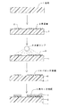
塩素化PPプライマー塗料 100重量部にエポキシ系アクリレートを固形分で15重量部混合した塗料(「プラニット#543」大日本塗料製)を用意し、図1に示すように、ブタジエン変性PP(トヨタスーパーオレフィンポリマー)から形成されマスキングされた基板1の表面にスプレー塗布し乾燥して、膜厚15μmの表面層2を形成した。
(Example 1)
Chlorinated PP primer paint A paint ("Planit # 543" manufactured by Dainippon Paint Co., Ltd.) prepared by mixing 15 parts by weight of epoxy acrylate with 100 parts by weight is prepared. As shown in FIG. The
マスキングを除去し、放射照度 170mW/cm2 の水銀ランプ3を用いて、基板1の表面層2が形成された表面に紫外線を照射した。ここで、紫外線の照射時間を0分,5分,10分,15分,20分,25分,30分の7水準とし、それぞれの処理基板を得た。
Masking was removed, and the surface of the substrate 1 on which the
次いで、NaOH(アルカリ成分)50g/Lと、ラウリル硫酸ナトリウム(陰イオン性界面活性剤)1g/Lと、を溶解した混合水溶液を60℃に加熱し、そこへオゾン溶液処理後の各基板1をそれぞれ2分間浸漬した。 Next, a mixed aqueous solution in which NaOH (alkali component) 50 g / L and sodium lauryl sulfate (anionic surfactant) 1 g / L are dissolved is heated to 60 ° C., and each substrate 1 after the ozone solution treatment is added thereto. Each was immersed for 2 minutes.
これらを水洗・乾燥後、3N塩酸水溶液に塩化パラジウムを 0.1重量%溶解し塩化錫を5重量%溶解して50℃に加熱された触媒溶液中に3分間浸漬し、次いでパラジウムを活性化するために、1N塩酸水溶液に3分間浸漬した。これにより触媒が吸着した基板1を得た。 In order to activate palladium by rinsing with water and drying, 0.1% by weight of palladium chloride in 5N aqueous hydrochloric acid and 5% by weight of tin chloride were dissolved in a catalyst solution heated to 50 ° C. for 3 minutes. And immersed in a 1N aqueous hydrochloric acid solution for 3 minutes. Thereby, the substrate 1 on which the catalyst was adsorbed was obtained.
その後、40℃に保温されたNi−P化学めっき浴中に触媒が吸着した基板1を浸漬し、10分間Ni−Pめっき被膜4を析出させた。析出したNi−Pめっき被膜4の厚さは 0.5μmである。続いて硫酸銅系Cu電解めっき浴にて、Ni−Pめっき被膜4の表面に銅めっき被膜5を 100μm析出させた。なお基板1の表面層2を除く表面には、Ni−Pめっき被膜4が析出しなかったので、銅めっき被膜5も形成されなかった。
Thereafter, the substrate 1 on which the catalyst was adsorbed was immersed in a Ni—P chemical plating bath kept at 40 ° C., and the Ni—P plating film 4 was deposited for 10 minutes. The thickness of the deposited Ni—P plating film 4 is 0.5 μm. Subsequently, 100 μm of a
銅めっき被膜5の形成後、70℃で2時間乾燥した。その後、得られた銅めっき被膜5に基板1に達する切り込みを1cm幅で入れ、引張り試験機にてめっき被膜の付着強度をそれぞれ測定した。結果を表1に示す。
After forming the
(比較例1)
表面層2を形成しない基板1を用いたこと以外は実施例1と同様にして、各時間の紫外線照射を行い、同様にNi−P化学めっき処理と硫酸銅系Cu電解めっき処理を行った。そして同様に付着強度を測定し、結果を表1に示す。
(Comparative Example 1)
Except having used the board | substrate 1 which does not form the
<評価> <Evaluation>
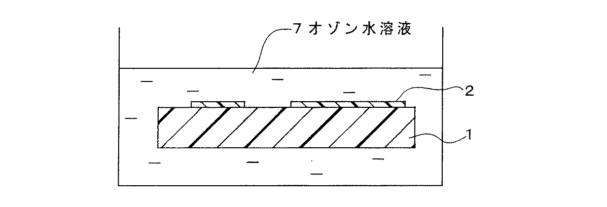
表1より、実施例1では10分間以上の紫外線処理によってめっき被膜が形成されたのに対し、比較例1ではめっき被膜がほとんど析出していないことがわかる。すなわち表面層2を形成して紫外線を照射することで、無電解めっき被膜を形成することができ、しかも紫外線照射時間を20分以上とすることでめっき被膜の高い付着性が発現することが明らかである。
From Table 1, it can be seen that in Example 1, the plating film was formed by ultraviolet treatment for 10 minutes or more, whereas in Comparative Example 1, the plating film was hardly deposited. That is, it is clear that an electroless plating film can be formed by forming the
(実施例2)
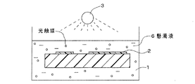
実施例1と同様の表面層2が形成された基材1を用意し、水1リットル中にアナターゼ型TiO2(半導体光触媒)粉末0.05gを懸濁させた懸濁液6中に浸漬した。そして放射照度 170mW/cm2 の水銀ランプ3を用い、図2に示すように、懸濁液6の液面上から基板1の表面層2が形成された表面に紫外線を照射した。ここで、紫外線の照射時間を0分,5分,10分,15分,20分,25分,30分の7水準とし、それぞれの処理基板を得た。
(Example 2)
A base material 1 having a
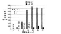
その後、実施例1と同様にしてアルカリ処理と触媒吸着処理を行い、同様にしてNi−Pめっき被膜4と銅めっき被膜5を形成した後、同様にしてめっき被膜の付着強度をそれぞれ測定した。結果を表2及び図3に示す。
Thereafter, the alkali treatment and the catalyst adsorption treatment were performed in the same manner as in Example 1, and after forming the Ni-P plating film 4 and the
(比較例2)
表面層2を形成しない基板1を用いたこと以外は実施例2と同様にして、各時間の光触媒−紫外線照射処理を行い、同様にNi−P化学めっき処理と硫酸銅系Cu電解めっき処理を行った後、同様にしてめっき被膜の付着強度をそれぞれ測定した。結果を表2及び図3に示す。
(Comparative Example 2)
Except having used the board | substrate 1 which does not form the
<評価> <Evaluation>
表2及び図3から、比較例2においても光触媒−紫外線照射処理時間が長くなれば無電解めっき被膜が析出しているものの、その付着強度は低い。しかし実施例2では、光触媒−紫外線照射処理時間が短くても無電解めっき被膜が析出し、処理時間が15分以上あれば十分な付着強度が発現されていることがわかり、これは表面層2を形成した効果であることが明らかである。また実施例1より短時間の処理で高い付着強度が発現していることから、光触媒の存在下で紫外線照射するのがより効果的であることが明らかである。 From Table 2 and FIG. 3, also in Comparative Example 2, although the electrocatalyst-ultraviolet irradiation treatment time is prolonged, the electroless plating film is deposited, but the adhesion strength is low. However, in Example 2, it can be seen that even when the photocatalyst-ultraviolet irradiation treatment time is short, the electroless plating film is deposited, and if the treatment time is 15 minutes or longer, sufficient adhesion strength is expressed. It is clear that this is the effect of forming. In addition, since high adhesion strength is manifested in a shorter time treatment than Example 1, it is clear that it is more effective to irradiate with ultraviolet rays in the presence of a photocatalyst.
(実施例3)
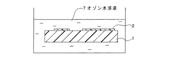
実施例1と同様の表面層2が形成された基材1を用意し、図4に示すように、150PPMのオゾンを含有するオゾン水溶液7に室温で20分間浸漬するオゾン溶液処理を行った。その後、実施例1と同様にしてアルカリ処理と触媒吸着処理を行い、同様にしてNi−Pめっき被膜4と銅めっき被膜5を形成した後、同様にしてめっき被膜の付着強度をそれぞれ測定した。付着強度の測定は、銅めっき被膜5の形成直後、銅めっき被膜5の形成から60分後、銅めっき被膜5の形成から 120分後にそれぞれ行った。結果を表3に示す。
(Example 3)
A base material 1 on which a
(実施例4)
実施例1と同様の表面層2が形成された基材1を用意し、放射照度 100mW/cm2 の水銀ランプを用いて、基板1の表面層2が形成された表面に紫外線を20分間照射した。その後、実施例1と同様にしてアルカリ処理と触媒吸着処理を行い、同様にしてNi−Pめっき被膜4と銅めっき被膜5を形成した後、実施例3と同様にしてめっき被膜の付着強度をそれぞれ測定した。結果を表3に示す。
Example 4
A base material 1 having the
(実施例5)
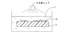
実施例1と同様の表面層2が形成された基材1を用意し、図5に示すように、150PPMのオゾンを含有するオゾン水溶液7に浸漬した状態で、放射照度 100mW/cm2 の水銀ランプ8を用いて、オゾン水溶液7の液面上から基板1の表面層2が形成された表面に紫外線を10分間照射した。その後、実施例1と同様にしてアルカリ処理と触媒吸着処理を行い、同様にしてNi−Pめっき被膜4と銅めっき被膜5を形成した後、実施例3と同様にしてめっき被膜の付着強度をそれぞれ測定した。結果を表3に示す。
(Example 5)
A substrate 1 on which a
(実施例6)
実施例1と同様の表面層2が形成された基材1を用意し、水1リットル中にアナターゼ型TiO2(半導体光触媒)粉末0.01gを懸濁させた懸濁液中に浸漬した。そして放射照度 100mW/cm2 の水銀ランプを用い、実施例2と同様に懸濁液の液面上から基板1の表面層2が形成された表面に紫外線を10分間照射した。
(Example 6)
A base material 1 having a
その後、実施例1と同様にしてアルカリ処理と触媒吸着処理を行い、同様にしてNi−Pめっき被膜4と銅めっき被膜5を形成した後、実施例3と同様にしてめっき被膜の付着強度をそれぞれ測定した。結果を表3に示す。
Thereafter, the alkali treatment and the catalyst adsorption treatment were performed in the same manner as in Example 1, and after the Ni-P plating film 4 and the
<評価> <Evaluation>
表3より、実施例3〜6のいずれも高い付着強度でめっき被膜を形成できていることがわかる。そしていずれの実施例でも銅めっき被膜5の形成後の放置時間が長いほど付着強度が増大しているが、オゾン溶液中で紫外線照射した実施例5、及び光触媒の共存下で紫外線照射した実施例6では、実施例3,4に比べて銅めっき被膜5の形成直後から高い付着強度が発現され、その効果はオゾン溶液中で紫外線照射した実施例5が特に高いことが明らかである。
From Table 3, it can be seen that any of Examples 3 to 6 can form a plating film with high adhesion strength. In any of the examples, the adhesion strength increases as the standing time after the formation of the
1:基板(素材本体) 2:表面層 3:無電解めっき被膜
4:銅めっき被膜 5:懸濁液 6:水銀ランプ
7:オゾン水溶液 8:水銀ランプ
1: Substrate (material body) 2: Surface layer 3: Electroless plating film 4: Copper plating film 5: Suspension 6: Mercury lamp 7: Ozone aqueous solution 8: Mercury lamp
Claims (14)
Priority Applications (1)
| Application Number | Priority Date | Filing Date | Title |
|---|---|---|---|
| JP2003350875A JP4314093B2 (en) | 2003-10-09 | 2003-10-09 | Plating material, method for producing the same, and method for producing plated coating member |
Applications Claiming Priority (1)
| Application Number | Priority Date | Filing Date | Title |
|---|---|---|---|
| JP2003350875A JP4314093B2 (en) | 2003-10-09 | 2003-10-09 | Plating material, method for producing the same, and method for producing plated coating member |
Publications (2)
| Publication Number | Publication Date |
|---|---|
| JP2005113236A true JP2005113236A (en) | 2005-04-28 |
| JP4314093B2 JP4314093B2 (en) | 2009-08-12 |
Family
ID=34542306
Family Applications (1)
| Application Number | Title | Priority Date | Filing Date |
|---|---|---|---|
| JP2003350875A Expired - Fee Related JP4314093B2 (en) | 2003-10-09 | 2003-10-09 | Plating material, method for producing the same, and method for producing plated coating member |
Country Status (1)
| Country | Link |
|---|---|
| JP (1) | JP4314093B2 (en) |
Cited By (8)
| Publication number | Priority date | Publication date | Assignee | Title |
|---|---|---|---|---|
| JP2006219715A (en) * | 2005-02-09 | 2006-08-24 | Ebara Udylite Kk | Metal plating method for heat-resistant insulating resin |
| JP2007239084A (en) * | 2006-03-13 | 2007-09-20 | Toyota Motor Corp | Electroless plating method |
| KR100828721B1 (en) | 2006-02-04 | 2008-05-09 | 주식회사 엘지화학 | Surface Polarization Method of Hydrophobic Resin Fine Particles |
| JP2011063854A (en) * | 2009-09-17 | 2011-03-31 | Toyota Industries Corp | Method for manufacturing base material to be electroless-plated |
| JP2011063855A (en) * | 2009-09-17 | 2011-03-31 | Toyota Industries Corp | Method for manufacturing base material to be electroless-plated |
| JP2014118623A (en) * | 2012-12-19 | 2014-06-30 | Kanto Gakuin | Method for producing plating film |
| JP5856354B1 (en) * | 2014-12-08 | 2016-02-09 | キヤノン・コンポーネンツ株式会社 | Resin product with plating film, resin product, and method for producing resin product with plating film |
| JP2016121387A (en) * | 2014-12-25 | 2016-07-07 | キヤノン・コンポーネンツ株式会社 | Production method of resin product with plating film |
-
2003
- 2003-10-09 JP JP2003350875A patent/JP4314093B2/en not_active Expired - Fee Related
Cited By (10)
| Publication number | Priority date | Publication date | Assignee | Title |
|---|---|---|---|---|
| JP2006219715A (en) * | 2005-02-09 | 2006-08-24 | Ebara Udylite Kk | Metal plating method for heat-resistant insulating resin |
| KR100828721B1 (en) | 2006-02-04 | 2008-05-09 | 주식회사 엘지화학 | Surface Polarization Method of Hydrophobic Resin Fine Particles |
| JP2007239084A (en) * | 2006-03-13 | 2007-09-20 | Toyota Motor Corp | Electroless plating method |
| JP2011063854A (en) * | 2009-09-17 | 2011-03-31 | Toyota Industries Corp | Method for manufacturing base material to be electroless-plated |
| JP2011063855A (en) * | 2009-09-17 | 2011-03-31 | Toyota Industries Corp | Method for manufacturing base material to be electroless-plated |
| US8563093B2 (en) | 2009-09-17 | 2013-10-22 | Toyota Jidosha Kabushiki Kaisha | Method for production of electroless plating material |
| JP2014118623A (en) * | 2012-12-19 | 2014-06-30 | Kanto Gakuin | Method for producing plating film |
| JP5856354B1 (en) * | 2014-12-08 | 2016-02-09 | キヤノン・コンポーネンツ株式会社 | Resin product with plating film, resin product, and method for producing resin product with plating film |
| WO2016092584A1 (en) * | 2014-12-08 | 2016-06-16 | キヤノン・コンポーネンツ株式会社 | Resin product with plating film, and method for producing resin product and method for producing resin product with plating film |
| JP2016121387A (en) * | 2014-12-25 | 2016-07-07 | キヤノン・コンポーネンツ株式会社 | Production method of resin product with plating film |
Also Published As
| Publication number | Publication date |
|---|---|
| JP4314093B2 (en) | 2009-08-12 |
Similar Documents
| Publication | Publication Date | Title |
|---|---|---|
| JP4135459B2 (en) | Method for pretreatment of electroless plating material and method for manufacturing plating coated member | |
| JP2660002B2 (en) | Electroplating method | |
| CN100390319C (en) | Plating method for insulator articles | |
| JP2008031513A (en) | Metallization method for plastic surfaces | |
| JP4314093B2 (en) | Plating material, method for producing the same, and method for producing plated coating member | |
| JP4449246B2 (en) | Pretreatment method of electroless plating material | |
| JP3999696B2 (en) | Electroless plating method and plated parts | |
| US20060042954A1 (en) | Method for plating resin material | |
| JP2003193247A (en) | Pretreatment method for electroless plating material | |
| JP2007231362A (en) | Electroless plating method for resin products | |
| JP2005036292A (en) | Electroless plating method and plated parts | |
| JP4376575B2 (en) | Method for producing plating-coated member | |
| JP3897590B2 (en) | Pretreatment method of electroless plating material | |
| JP4332795B2 (en) | Electroless plating method | |
| JP2005146330A (en) | Surface treatment method for non-conductor material | |
| JP4372491B2 (en) | Method for producing plating-coated member | |
| JP6130331B2 (en) | Manufacturing method of resin product with metal film | |
| JP7160306B2 (en) | Electroless plating pretreatment composition, electroless plating pretreatment method, electroless plating method | |
| JP2005217040A (en) | Manufacturing method of flexible wiring board | |
| HK1231141B (en) | Resin plating method |
Legal Events
| Date | Code | Title | Description |
|---|---|---|---|
| A621 | Written request for application examination |
Free format text: JAPANESE INTERMEDIATE CODE: A621 Effective date: 20060726 |
|
| A977 | Report on retrieval |
Free format text: JAPANESE INTERMEDIATE CODE: A971007 Effective date: 20080724 |
|
| A131 | Notification of reasons for refusal |
Free format text: JAPANESE INTERMEDIATE CODE: A131 Effective date: 20080729 |
|
| A521 | Written amendment |
Free format text: JAPANESE INTERMEDIATE CODE: A523 Effective date: 20080929 |
|
| A131 | Notification of reasons for refusal |
Free format text: JAPANESE INTERMEDIATE CODE: A131 Effective date: 20090210 |
|
| A521 | Written amendment |
Free format text: JAPANESE INTERMEDIATE CODE: A523 Effective date: 20090406 |
|
| TRDD | Decision of grant or rejection written | ||
| A01 | Written decision to grant a patent or to grant a registration (utility model) |
Free format text: JAPANESE INTERMEDIATE CODE: A01 Effective date: 20090507 |
|
| A01 | Written decision to grant a patent or to grant a registration (utility model) |
Free format text: JAPANESE INTERMEDIATE CODE: A01 |
|
| A61 | First payment of annual fees (during grant procedure) |
Free format text: JAPANESE INTERMEDIATE CODE: A61 Effective date: 20090518 |
|
| FPAY | Renewal fee payment (prs date is renewal date of database) |
Free format text: PAYMENT UNTIL: 20120522 Year of fee payment: 3 |
|
| FPAY | Renewal fee payment (prs date is renewal date of database) |
Free format text: PAYMENT UNTIL: 20120522 Year of fee payment: 3 |
|
| FPAY | Renewal fee payment (prs date is renewal date of database) |
Free format text: PAYMENT UNTIL: 20130522 Year of fee payment: 4 |
|
| FPAY | Renewal fee payment (prs date is renewal date of database) |
Free format text: PAYMENT UNTIL: 20140522 Year of fee payment: 5 |
|
| R250 | Receipt of annual fees |
Free format text: JAPANESE INTERMEDIATE CODE: R250 |
|
| LAPS | Cancellation because of no payment of annual fees |