JP5083005B2 - Resin substrate having a precious metal fixed on the surface layer, its manufacturing method, circuit board, and its manufacturing method - Google Patents
Resin substrate having a precious metal fixed on the surface layer, its manufacturing method, circuit board, and its manufacturing method Download PDFInfo
- Publication number
- JP5083005B2 JP5083005B2 JP2008104651A JP2008104651A JP5083005B2 JP 5083005 B2 JP5083005 B2 JP 5083005B2 JP 2008104651 A JP2008104651 A JP 2008104651A JP 2008104651 A JP2008104651 A JP 2008104651A JP 5083005 B2 JP5083005 B2 JP 5083005B2
- Authority
- JP
- Japan
- Prior art keywords
- resin
- noble metal
- resin substrate
- substrate
- composite layer
- Prior art date
- Legal status (The legal status is an assumption and is not a legal conclusion. Google has not performed a legal analysis and makes no representation as to the accuracy of the status listed.)
- Expired - Fee Related
Links
Images
Landscapes
- Coating Of Shaped Articles Made Of Macromolecular Substances (AREA)
- Laminated Bodies (AREA)
- Chemically Coating (AREA)
- Manufacturing Of Printed Wiring (AREA)
Description
本発明は、表層に貴金属を固定させた樹脂基板とその製造方法、表層に貴金属を固定させた樹脂基板からなる回路基板とその製造方法に関する。本発明の樹脂基板は、表層に貴金属を固定させているため、該貴金属が無電解めっきの核として作用し、微細配線が可能な回路基板とすることができる。 The present invention relates to a resin substrate having a noble metal fixed on a surface layer and a manufacturing method thereof, and a circuit substrate made of a resin substrate having a noble metal fixed to a surface layer and a manufacturing method thereof. Since the noble metal is fixed to the surface layer of the resin substrate of the present invention, the noble metal acts as a core of electroless plating, and a circuit board capable of fine wiring can be obtained.
一般に回路基板は、樹脂基板の表面に金属配線層を配置して回路基板とする。樹脂表面に無電解めっきにより金属被膜を形成する場合には、金属被膜と樹脂との付着強度が低く、金属被膜が剥離し易いという問題があった。そのため樹脂素材に対して化学的エッチング処理を行って表面を粗面化し、その後無電解めっき処理する工程が一般に行われている。しかしエッチングによって粗面化する方法では、表面平滑性が低下するとともに、クロム酸、硫酸などの毒劇物を用いる必要があり、廃液処理などに問題がある。 In general, a circuit board is formed by arranging a metal wiring layer on the surface of a resin substrate. When a metal film is formed on the resin surface by electroless plating, there is a problem that the adhesion strength between the metal film and the resin is low and the metal film is easily peeled off. Therefore, a chemical etching process is generally performed on the resin material to roughen the surface, and then a process of electroless plating is generally performed. However, in the method of roughening by etching, the surface smoothness is deteriorated, and it is necessary to use poisonous and deleterious substances such as chromic acid and sulfuric acid.
そこで下記特許文献1には、樹脂素材をオゾン溶液に接触させた後、界面活性剤とアルカリ成分とを含む溶液で処理し、その後に無電解めっきを行うことが記載されている。この方法によれば、オゾンによる酸化によって樹脂素材表面の二重結合が切断され、極性基が生成される。またアルカリ成分によって脆化層が除去され、界面活性剤が極性基に吸着する。そして無電解めっきに先立つ触媒処理時には、極性基に吸着している界面活性剤に触媒が吸着するため、無電解めっき時に金属が極性基に結合しやすくなり、無電解めっき被膜の付着性が向上する。 Therefore, Patent Document 1 below describes that after a resin material is brought into contact with an ozone solution, the resin material is treated with a solution containing a surfactant and an alkali component, and then electroless plating is performed. According to this method, the double bond on the surface of the resin material is cut by oxidation with ozone, and a polar group is generated. Further, the brittle layer is removed by the alkali component, and the surfactant is adsorbed on the polar group. During the catalyst treatment prior to electroless plating, the catalyst is adsorbed to the surfactant adsorbed on the polar group, so that the metal is easily bonded to the polar group during electroless plating, and the adhesion of the electroless plating film is improved. To do.
また、下記特許文献2には、光触媒粉末を懸濁させた液に樹脂素材を浸漬し、液中で光を照射することで、樹脂素材の表面に極性基を形成し、その後無電解めっきする方法が記載されている。この方法によっても、無電解めっき被膜の付着性が向上する。 In Patent Document 2 below, a resin material is immersed in a liquid in which a photocatalyst powder is suspended, and light is irradiated in the liquid to form polar groups on the surface of the resin material, followed by electroless plating. A method is described. This method also improves the adhesion of the electroless plating film.
更に、下記特許文献3には、極性基を有するマトリックス形成性物質における極性基の反応を経て形成された化合物を少なくとも含むマトリックスと、その反応の結果、極性基との相互作用の消失又は減少によりマトリックス中に析出して分散した金属微粒子と、を有する導電性被調整体が記載されている。しかしこの方法は、基体に液状体を塗布した後に真空下で加熱保持することで導電性被調整体を形成するものであり、導電性被調整体と基体との付着性の信頼性が低い。また反応に長時間必要であり、生産性が低いという問題もある。 Further, in Patent Document 3 below, a matrix containing at least a compound formed through a reaction of a polar group in a matrix-forming substance having a polar group, and as a result of the reaction, the interaction with the polar group is lost or reduced. A conductive conditioned body having metal fine particles deposited and dispersed in a matrix is described. However, in this method, the liquid to be adjusted is formed by applying the liquid to the substrate and then heating and holding it under vacuum, so that the reliability of the adhesion between the substrate to be adjusted and the substrate is low. There is also a problem that the reaction requires a long time and productivity is low.
そこで、下記特許文献4には、導電性、耐摩耗性などの特性を有する樹脂基体を提供することを目的として、樹脂マトリックス中に微細な金属粒子が均一に分散してなる樹脂−金属コンポジット層が、樹脂基体の表面に一体的に形成された樹脂基板が開示されている。ここで、樹脂−金属コンポジット層の厚さは、20〜2000nmであることが望ましいとされている。また該樹脂基板の製造法として、樹脂基体の表面に極性基をもつ改質層を形成する前処理工程と、改質層に金属化合物溶液を接触させ金属のコロイド及びイオンの少なくとも一方を極性基に吸着させ改質層に金属微粒子を分散させる吸着工程とを、この順で行うことが開示されている。 Therefore, Patent Document 4 listed below discloses a resin-metal composite layer in which fine metal particles are uniformly dispersed in a resin matrix for the purpose of providing a resin substrate having characteristics such as conductivity and wear resistance. However, a resin substrate integrally formed on the surface of a resin substrate is disclosed. Here, the thickness of the resin-metal composite layer is preferably 20 to 2000 nm. Further, as a method for producing the resin substrate, a pretreatment step for forming a modified layer having a polar group on the surface of the resin substrate, a metal compound solution is brought into contact with the modified layer, and at least one of the metal colloid and ions is polar group It is disclosed that an adsorption step of adsorbing to a modified layer and dispersing fine metal particles in a modified layer is performed in this order.
小型高密度部品や高周波回路では、基板配線間隔が狭い(間隔100μm以下、従来は100μm以上)ことや、高周波特性のため平滑性(Rz≦2μm、従来はRz≧5μm程度)の要求がされる。しかし、特許文献4に開示された樹脂基板では、
(1)基板狭小配線間の200nm以上のコンポジット層は後工程のエッチンゲで除去されず、絶縁不良の原因となる。
(2)逆にコンポジット層が薄い(10〜200nm)と平滑樹脂上では十分な密着強度が得られにくい。
という問題が存在した。
Small high-density components and high-frequency circuits require a narrow board wiring interval (interval of 100 μm or less, conventionally 100 μm or more), and smoothness (Rz ≦ 2 μm, conventional Rz ≧ 5 μm) due to high-frequency characteristics. . However, in the resin substrate disclosed in Patent Document 4,
(1) The composite layer of 200 nm or more between the narrow wirings of the substrate is not removed by the subsequent etching process, which causes insulation failure.
(2) Conversely, if the composite layer is thin (10 to 200 nm), it is difficult to obtain sufficient adhesion strength on the smooth resin.
There was a problem.
このように、(1)コンポジット層が厚い(200nm以上)場合は、狭小配線間のコンポジット層は後工程のエッチングで除去する必要があるが、樹脂内にめっきが入込んでいる構造上、エッチングされにくいため、厚すぎると深い部分の層が除去しきれないこと、(2)コンポジット層が薄い(10〜200nm)場合は、コンポジット層が薄いと平滑樹脂上では十分なめっき密着力が得られにくく、密着力確保のために、新たなめっき密着力向上の対策との併用が必要となる。 Thus, (1) when the composite layer is thick (200 nm or more), it is necessary to remove the composite layer between the narrow wirings by etching in a later process, but etching is performed due to the structure in which the plating is embedded in the resin. If the layer is too thick, the deep layer cannot be removed. (2) When the composite layer is thin (10 to 200 nm), if the composite layer is thin, sufficient plating adhesion can be obtained on the smooth resin. It is difficult, and in order to secure adhesion, it is necessary to use it together with a new measure for improving plating adhesion.
本発明はこのような事情に鑑みてなされたものであり、樹脂表層に銅などのめっきと樹脂がナノメートルオーダーで混在する層を持ち、平滑樹脂上で非常に高いめっき密着性を有するに用いられる樹脂基板であって、平滑樹脂上に高密着強度のめっきを実施できるため、微細配線基板や高周波特性に優れたプリント配線基板を作製することを目的とする。 The present invention has been made in view of such circumstances, and has a resin surface layer in which plating such as copper and a resin are mixed in a nanometer order, and is used for having very high plating adhesion on a smooth resin. An object of the present invention is to produce a fine wiring board and a printed wiring board excellent in high-frequency characteristics because it can be plated with high adhesion strength on a smooth resin.
本発明者らは、貴金属を補足する成分を含む樹脂材料を用い、オゾン水処理で従来比で薄い混在層(ナノコンポジット層)でも平滑樹脂上で非常に高いめっき密着性を有する、微細配線基板や高周波特性に優れた基板に最適な樹脂基板を開発した。 The present inventors use a resin material containing a component supplementing a noble metal, and have a very high plating adhesion on a smooth resin even with a mixed layer (nanocomposite layer) that is thinner than conventional by ozone water treatment. We have developed a resin substrate that is optimal for substrates with excellent high-frequency characteristics.
即ち、第1に、本発明は、樹脂基板の発明であり、樹脂基体と、該樹脂基体の表層に一体的に形成され樹脂マトリックス中に微細な金属粒子が均一に分散してなる樹脂−金属コンポジット層を有し、該樹脂マトリックス中にトリアジン環を有することを特徴とする。 That is, first, the present invention is an invention of a resin substrate, and is a resin-metal formed integrally with a resin substrate and a surface layer of the resin substrate, and fine metal particles are uniformly dispersed in the resin matrix. It has a composite layer and has a triazine ring in the resin matrix.
本発明の樹脂基板の樹脂−金属コンポジット層の厚さは10〜200nmであることが好ましい。 The thickness of the resin-metal composite layer of the resin substrate of the present invention is preferably 10 to 200 nm.
又、本発明の樹脂基板は、後で無電解めっきを行うための核となる貴金属がトリアジン環に固定されたことが好ましい。 Moreover, it is preferable that the noble metal used as the nucleus for performing electroless plating later on the resin substrate of this invention was fixed to the triazine ring.
第2に、本発明は、上記の樹脂基板の製造方法の発明であり、シアネート系ビルトアップ樹脂を熱処理し樹脂中にトリアジン環を生成させる工程と、オゾン水により樹脂基体の表層を改質すると共に、貴金属錯イオン又はコロイドタイプの貴金属を含むキャタリスト液に浸漬し、樹脂マトリックス中に微細な金属粒子が均一に分散してなる樹脂−金属コンポジット層を樹脂基体と一体的に形成し、貴金属をトリアジン環によって固定させる工程とを有することを特徴とする。 2ndly, this invention is invention of the manufacturing method of said resin substrate, modify | reforms the surface layer of a resin base | substrate with the process which heat-processes cyanate-type built-up resin, and produces | generates a triazine ring in resin, and ozone water A resin-metal composite layer in which fine metal particles are uniformly dispersed in a resin matrix is integrally formed with a resin substrate by being immersed in a catalyst liquid containing a noble metal complex ion or a colloid type noble metal. And fixing with a triazine ring.
第3に、本発明は、上記の樹脂基板を用いた回路基板の発明であり、樹脂基体と、該樹脂基体の表面に一体的に形成され樹脂マトリックス中に微細な金属粒子が均一に分散してなる樹脂−金属コンポジット層とからなり、該樹脂マトリックス中にトリアジン環を有する樹脂−金属コンポジット層をもつ樹脂基板上に金属配線層が配置されたことを特徴とする。 Third, the present invention is an invention of a circuit board using the above-mentioned resin substrate, in which fine resin particles are uniformly dispersed in a resin matrix and a resin matrix formed integrally on the surface of the resin substrate. A metal wiring layer is disposed on a resin substrate having a resin-metal composite layer having a triazine ring in the resin matrix.
第4に、本発明は、上記の回路基板の製造方法の発明であり、シアネート系ビルトアップ樹脂を熱処理し樹脂中にトリアジン環を生成させる工程と、オゾン水により樹脂基体の表層を改質すると共に、貴金属錯イオン又はコロイドタイプの貴金属を含むキャタリスト液に浸漬し、樹脂マトリックス中に微細な金属粒子が均一に分散してなる樹脂−金属コンポジット層を一体的に形成し、貴金属をトリアジン環によって固定させる工程とによって樹脂基板を製造し、該貴金属を核として樹脂基板の表面に無電解めっきにより金属被膜を形成し、その後に該金属被膜を除去することを特徴とする。 Fourthly, the present invention is an invention of the above-described method for producing a circuit board, in which a cyanate built-up resin is heat-treated to form a triazine ring in the resin, and the surface layer of the resin substrate is modified with ozone water. At the same time, it is immersed in a catalyst liquid containing a noble metal complex ion or colloid type noble metal, and a resin-metal composite layer in which fine metal particles are uniformly dispersed in a resin matrix is integrally formed. A resin substrate is manufactured by the step of fixing by the above-described method, a metal film is formed on the surface of the resin substrate by electroless plating using the noble metal as a nucleus, and then the metal film is removed.
本発明により、薄いコンポジット層でも高めっき密着強度を有する平滑な樹脂基板が得られる。樹脂表層に銅めっきと樹脂がナノメールオーダーで混在する層を持つプリント配線基板に好適に用いられる。ナノコンポジット層が厚いと後工程のエッチンゲで除去しきれず、絶縁不良の原因となるが、本発明では、貴金属を補足する成分を含む樹脂材料を用い且つオゾン水で処理することで、薄いナノコンポジット層でも平滑樹脂上で非常に高いめっき密着性を有する。平滑樹脂基板上に高密着強度のめっきを実施できるため、微細配線基板や高周波特性に優れた回路基板を作製できる。 According to the present invention, a smooth resin substrate having high plating adhesion strength can be obtained even with a thin composite layer. It is suitably used for a printed wiring board having a layer in which copper plating and resin are mixed in nano mail order on the resin surface layer. If the nanocomposite layer is thick, it cannot be completely removed by subsequent etching and causes insulation failure. However, in the present invention, a thin nanocomposite is obtained by using a resin material containing a component supplementing a noble metal and treating with ozone water. Even the layer has very high plating adhesion on the smooth resin. Since plating with high adhesion strength can be performed on a smooth resin substrate, a fine wiring substrate and a circuit substrate excellent in high-frequency characteristics can be manufactured.
本発明では、シアネート系ビルドアップ樹脂に所定条件で熱処理を実施する。反応により樹脂中にトリアジンを形成させる。該トリアジンが貴金属成分を固定化する性質を有する。 In the present invention, the cyanate buildup resin is heat-treated under predetermined conditions. Triazine is formed in the resin by reaction. The triazine has a property of immobilizing a noble metal component.
本発明では、オヅン水処理により、樹脂の表層を改質する。改質により樹脂表層に液体の浸透性が向上する。また、オゾン水による樹脂のエッチンゲで樹脂表面に微小な凹凸を形成させる。ここで、オゾン水処理とは、オゾンガスを溶解させた水中に樹脂を浸漬させる処理のことである。 In the present invention, the surface layer of the resin is modified by on-water treatment. By the modification, the liquid permeability to the resin surface layer is improved. Moreover, minute unevenness is formed on the resin surface by etching of the resin with ozone water. Here, the ozone water treatment is a treatment in which a resin is immersed in water in which ozone gas is dissolved.
本発明では、化学銅めっきの前処理液(クリーナコンディショナー、プリディップ、キャタリスト、還元液)が樹脂表層に浸透する。トリアジンの作用でPd触媒(化学銅めっきの析出核)が樹脂表層に吸着、固定化されやすくなり、Pd密度の高い層が形成される。 In the present invention, a chemical copper plating pretreatment solution (cleaner conditioner, pre-dip, catalyst, reducing solution) penetrates the resin surface layer. By the action of triazine, the Pd catalyst (precipitation nuclei of chemical copper plating) is easily adsorbed and immobilized on the resin surface layer, and a layer having a high Pd density is formed.
本発明では、化学銅めっき液が樹脂表層に浸透し、Pdを核に化学銅めっきが析出する。高密度にPdが存在するため、化学銅めっきが層内のナノオーダーの隙間にしっかりと析出する。また、PdやCuめっきが樹脂と強く固定化されている。相乗効果により樹脂とのめっき密着強度が高まる。コンポジット層が薄くても、平滑樹脂上に高い密着強度を有している樹脂基板が形成できる。 In the present invention, the chemical copper plating solution penetrates into the resin surface layer, and the chemical copper plating is deposited using Pd as a nucleus. Since Pd is present at a high density, chemical copper plating is firmly deposited in nano-order gaps in the layer. Moreover, Pd and Cu plating are strongly fixed to the resin. The plating adhesion strength with the resin is increased by the synergistic effect. Even if the composite layer is thin, a resin substrate having high adhesion strength can be formed on the smooth resin.
本発明で用いられる樹脂基体としては、ABS樹脂、AS樹脂、ポリスチレン樹脂、ポリオレフィン系樹脂、エポキシ樹脂、AN樹脂、ポリアミド樹脂、ポリエステル樹脂、PET樹脂、ポリアセタール樹脂、アクリル樹脂、ポリカーボネート樹脂、PMMA樹脂、セルロース系樹脂、フッ素樹脂、POM樹脂、PBT樹脂、ポリイミド樹脂、変成PPO樹脂、ポリフェニルサルファイド樹脂、シリコーン樹脂、ポリウレタン樹脂、フェノール樹脂、エラストマーとPPを含むポリマーアロイなど、各種の熱可塑性樹脂あるいは熱硬化性樹脂を用いることができる。また形状は制限されず、各種形状の成形品から樹脂基体を構成することができる。 Examples of the resin substrate used in the present invention include ABS resin, AS resin, polystyrene resin, polyolefin resin, epoxy resin, AN resin, polyamide resin, polyester resin, PET resin, polyacetal resin, acrylic resin, polycarbonate resin, PMMA resin, Various thermoplastic resins such as cellulose resin, fluororesin, POM resin, PBT resin, polyimide resin, modified PPO resin, polyphenyl sulfide resin, silicone resin, polyurethane resin, phenol resin, polymer alloy including elastomer and PP, or heat A curable resin can be used. Further, the shape is not limited, and the resin substrate can be formed from molded products having various shapes.
樹脂−金属コンポジット層は、樹脂基体を構成する樹脂マトリックス中に微細な金属粒子が均一に分散してなるものである。この金属としては、Pd、Au、Ag、Pt、Rh、Irなどの貴金属から種々選択することができる。 The resin-metal composite layer is formed by uniformly dispersing fine metal particles in a resin matrix constituting a resin substrate. This metal can be variously selected from noble metals such as Pd, Au, Ag, Pt, Rh, and Ir.
オゾン処理に用いるオゾン溶液中のオゾン濃度は、樹脂基体表面の活性化に大きく影響を及ぼし、10ppm程度から活性化の効果が見られるが、100ppm以上とすればその活性化の効果が飛躍的に高まり、より短時間の処理が可能である。また濃度が低いと劣化が先行するので、オゾン濃度は高い方が好ましい。オゾン溶液中のオゾンによる酸化によってオゾナイドが形成され、C‐OH結合又はC=O結合などの極性基が生成すると考えられる。 The ozone concentration in the ozone solution used for the ozone treatment greatly affects the activation of the surface of the resin substrate, and the activation effect is seen from about 10 ppm, but if it is 100 ppm or more, the activation effect is dramatically increased. The processing can be performed in a shorter time. Moreover, since deterioration precedes when the density | concentration is low, the one where an ozone density | concentration is high is preferable. Ozonide is formed by oxidation with ozone in an ozone solution, and it is considered that polar groups such as C—OH bond or C═O bond are generated.
オゾン溶液は、通常は水を溶媒とするが、有機又は無機の極性溶媒を溶媒とすることが好ましい。これにより処理時間をさらに短縮することが可能となる。有機極性溶媒としては、メタノール,エタノール,イソプロピルアルコールなどのアルコール類、N,N‐ジメチルホルムアミド、N,N‐ジメチルアセトアミド、ジメチルスルホキシド、N‐メチルピロリドン、ヘキサメチルホスホルアミド、蟻酸,酢酸などの有機酸類、あるいはこれらを水やアルコール系溶媒と混合したものが例示される。また無機極性溶媒としては、硝酸,塩酸,フッ化水素酸などの無機酸が例示される。 The ozone solution usually uses water as a solvent, but preferably uses an organic or inorganic polar solvent as a solvent. As a result, the processing time can be further shortened. Organic polar solvents include alcohols such as methanol, ethanol, isopropyl alcohol, N, N-dimethylformamide, N, N-dimethylacetamide, dimethylsulfoxide, N-methylpyrrolidone, hexamethylphosphoramide, formic acid, acetic acid, etc. Examples include organic acids, or a mixture of these with water or an alcohol solvent. Examples of the inorganic polar solvent include inorganic acids such as nitric acid, hydrochloric acid, and hydrofluoric acid.
樹脂基体をオゾン溶液と接触させるには、樹脂基体表面にオゾン溶液をスプレーする方法、樹脂基体をオゾン溶液中に浸漬する方法などがある。樹脂基体をオゾン溶液中に浸漬する方法によれば、スプレーによる接触に比べてオゾン溶液からオゾンが離脱し難いので好ましい。 In order to bring the resin substrate into contact with the ozone solution, there are a method of spraying the ozone solution on the surface of the resin substrate, a method of immersing the resin substrate in the ozone solution, and the like. The method of immersing the resin substrate in the ozone solution is preferable because ozone is less likely to be detached from the ozone solution compared to the contact by spraying.
貴金属吸着工程後に、樹脂−金属コンポジット層の表面に無電解めっきにより金属被膜を形成し、その後に形成されためっき被膜を除去することができる。無電解めっき処理では、吸着工程で形成された金属粒子を触媒として金属が析出して成長するので、樹脂−金属コンポジット層においては金属粒子の表面をめっき金属が覆う状態となり、金属粒子は二層構造の比較的大きな粒子となる。また樹脂−金属コンポジット層の表面には、無電解めっき被膜が形成される。 After the noble metal adsorption step, a metal film can be formed on the surface of the resin-metal composite layer by electroless plating, and the plating film formed thereafter can be removed. In the electroless plating treatment, metal deposits and grows using the metal particles formed in the adsorption process as a catalyst. Therefore, in the resin-metal composite layer, the surface of the metal particles is covered with the plating metal, and the metal particles are in two layers. The particles are relatively large in structure. An electroless plating film is formed on the surface of the resin-metal composite layer.
その後、めっき被膜を除去することで、樹脂−金属コンポジット層が表出する。この樹脂−金属コンポジット層は、コンポジット層の厚さが厚いもの、もしくは金属粒子の濃度が高いものは、受動部品内蔵基板などとして利用するのに好適である。 Then, the resin-metal composite layer is exposed by removing the plating film. The resin-metal composite layer having a thick composite layer or a high concentration of metal particles is suitable for use as a passive component built-in substrate or the like.
無電解めっき処理の条件、析出させる金属種などは制限されず、従来の無電解めっき処理と同様に行うことができる。そしてめっき被膜を除去するには、研磨など物理的な除去法、酸エッチング、逆電解法で溶解する方法などを利用することができる。なお、樹脂−金属コンポジット層まで除去しないように、条件を設定する必要がある。 The conditions for the electroless plating treatment, the metal species to be deposited, and the like are not limited, and can be performed in the same manner as the conventional electroless plating treatment. In order to remove the plating film, a physical removal method such as polishing, a method of dissolving by acid etching or a reverse electrolysis method, or the like can be used. In addition, it is necessary to set conditions so as not to remove the resin-metal composite layer.
本発明により、下記の作用効果を奏する。
1.表層のナノコンポジット層により平滑樹脂上のめっき密着力が向上する。
2.上記1により平滑樹脂上に高密着性を有するめっき配線を持つプリント配線基板を作製できる。
3.上記2の基板は高周波特性に優れ、かつL/S=10/10μm以下の微細配線形成が可能となる。
The present invention has the following effects.
1. The surface nanocomposite layer improves plating adhesion on the smooth resin.
2. According to the above 1, a printed wiring board having a plated wiring having high adhesion on a smooth resin can be produced.
3. The above substrate 2 is excellent in high-frequency characteristics and can form fine wiring with L / S = 10/10 μm or less.
以下、本発明の実施例を示す。
1.芳香族シアネート化合物と芳香族エポキシ樹脂とを含む樹脂、球状シリカおよびメチルエチルケトンからなる樹脂基板を用意した。芳香族シアネート化合物(A)としてロンザジャパン(株)PrimsetBA230S、芳香族エポキシ樹脂(B)としてジャパンエポキシレジン(株)#828、コバルト(II)アセチルアセトナートの1%N,N−ジメチルホルムアミド溶液(C)を、A:B:C=38:58:4(重量比)で混合したのち、ガラスエポキシ基板上に厚さ50μmになるように塗布し、110℃で10分乾燥させた。
Examples of the present invention will be described below.
1. A resin substrate made of a resin containing an aromatic cyanate compound and an aromatic epoxy resin, spherical silica and methyl ethyl ketone was prepared. Lonza Japan Co., Ltd. Primeset BA230S as the aromatic cyanate compound (A), Japan Epoxy Resin Co., Ltd. # 828 as the aromatic epoxy resin (B), 1% N, N-dimethylformamide solution of cobalt (II) acetylacetonate ( C) was mixed at A: B: C = 38: 58: 4 (weight ratio), and then applied to a glass epoxy substrate to a thickness of 50 μm and dried at 110 ° C. for 10 minutes.
2.上記樹脂基板に190℃×10分で熱処理を施した。これをIR分析したところ、波数1560cm−1のピークが増加し、トリアジン環が形成していると考えられる。 2. The resin substrate was heat treated at 190 ° C. for 10 minutes. When this was subjected to IR analysis, the peak at a wave number of 1560 cm −1 increased, and it is considered that a triazine ring was formed.
なお、熱処理条件の範囲は、150〜190℃で10〜30分が望ましい。150℃以下の温度や10分以下の短時間では、樹脂の硬化状態が不足し、後述のオゾン水に含浸した際に樹脂表面が過剰に酸化溶解して樹脂が弱くなるため、めっき皮膜の密着強度が低下する。190℃以上の温度や30分以上の熱処理後でも、めっき皮膜の密着強度が低下するが、その原因は、めっき後に硬化収縮することで作用していためっきのアンカー効果がめっき前に硬化が終了してしまうために作用しなくなるためと考えられる。 In addition, as for the range of heat processing conditions, 10 to 30 minutes are desirable at 150-190 degreeC. At a temperature of 150 ° C. or less or for a short time of 10 minutes or less, the cured state of the resin is insufficient, and when impregnated with ozone water described later, the resin surface is excessively oxidized and dissolved to weaken the resin. Strength decreases. Even after a temperature of 190 ° C or higher or a heat treatment of 30 minutes or more, the adhesion strength of the plating film is reduced, but the cause is that the plating anchor effect that worked by hardening shrinkage after plating has finished hardening before plating This is thought to be because it stops working.
3.この樹脂基板を40ppmのオゾンを含有する水溶液に含浸し、室温で12分間保持した。 3. This resin substrate was impregnated with an aqueous solution containing 40 ppm of ozone and kept at room temperature for 12 minutes.
4.オヅン水に含浸した基板を65℃に加温した処理液(奥野製薬工業社製OPC370コンディクリーンM)に5分間浸漬した。 4). The substrate impregnated with on water was immersed for 5 minutes in a treatment liquid heated to 65 ° C. (OPC370 Condy Clean M manufactured by Okuno Pharmaceutical Co., Ltd.).
5.上記樹脂基板を過硫酸ソーダと硫酸の混合水溶液にて処理した。 5). The resin substrate was treated with a mixed aqueous solution of sodium persulfate and sulfuric acid.
6.上記樹脂基板を水洗・乾燥後、Pd錯イオンを含むアルカリ性キャタリスト(奥野製薬工業社製OPC50インデューサA及びC)に40℃で5分間浸漬し、ついでPd還元液(奥野製薬工業竹製OPC150クリスターMU)に室温で6分間浸漬した。 6). The resin substrate is washed with water and dried, and then immersed in an alkaline catalyst containing Pd complex ions (OPC50 inducers A and C manufactured by Okuno Seiyaku Kogyo Co., Ltd.) at 40 ° C. for 5 minutes, and then a Pd reducing solution (OPC150 manufactured by Okuno Pharmaceutical Industrial Co., Ltd.). (Cryster MU) was immersed for 6 minutes at room temperature.
7.上記基板を32℃に保温した化学銅めっき液(奥野製薬工莱社製ATSアドカッバーW、還元剤ホルムアルデヒド2g/Lに浸漬し、30分間Cuめっき皮膜を析出させた。析出したCuめっき皮膜は0.5μmの厚さであった。 7). A chemical copper plating solution (ATS Advertor W manufactured by Okuno Seiyaku Kogyo Co., Ltd., reducing agent formaldehyde 2 g / L) was immersed in the above-mentioned substrate at a temperature of 32 ° C. to deposit a Cu plating film for 30 minutes. The thickness was 5 μm.
8.ついで、銅めっき浴中にて、電流密度3A/dm2を45分間印加し、25μmのめっき皮膜を形成した。 8). Next, a current density of 3 A / dm 2 was applied for 45 minutes in a copper plating bath to form a 25 μm plating film.
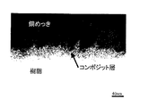
図1に、実施例で得られた銅めっき基板の断面写真を示す。樹脂基体上のコンポジット層と銅めっき層が見られる。 In FIG. 1, the cross-sectional photograph of the copper plating board | substrate obtained in the Example is shown. A composite layer and a copper plating layer on the resin substrate can be seen.
本発明は上記の実施例に限定されず、下記のような形態がある。
[コンポジット層の形成]
1)化学銅めっきの触媒核となる貴金属はPdに限らず、例えばAg触媒なども可能である。
2)めっきの種類はCuめっきに限らず、例えばNiめっきなども可能である。
3)Pdのキャタリストの種類は特に限定はない。ただし、触媒の粒径が小さいアルカリ性キャタリストがコロイド状の酸性キャタリストに比べ、樹脂表層(オゾン水による改質層)への浸透性、分散性が良いため高い密着強度が発現しやすい。
4)オゾン水処理は処理対象物の浸漬方式には限定されず、例えばスプレー式の処理でも可能である。
5)オゾン水処理前に有機溶媒を溶かした溶媒に浸漬させる、または、極性溶媒中でオゾン処理しても良い。極性溶媒の作用で樹脂がエッチングされやすくなり、オゾン水処理が、より低濃度で効率的に実施できる。ただし溶媒はオゾンで分解されにくいものが良い。
6)樹脂中に貴金属固定化成分を予め持っていても良いし、反応により形成させても良い。固定化成分を分散させた薬液中に樹脂を浸漬させ、浸透により樹脂に付与させても良い。また、実施例で実施している熱処理は、オゾン水処理前に限定されず、化学銅めっき前ならば良い。
7)めっき前処理の薬液は特に限定されない。
8)めっき液についても特に限定されない。
9)化学銅めっきの前処理液であるキャタリスト液には、貴金属錯イオンでなくコロイドタイプの貴金属が含まれていても良い。
The present invention is not limited to the above-described embodiments, and has the following forms.
[Formation of composite layer]
1) The noble metal that becomes the catalyst core of chemical copper plating is not limited to Pd, and for example, an Ag catalyst or the like is also possible.
2) The type of plating is not limited to Cu plating, and Ni plating, for example, is also possible.
3) There is no particular limitation on the type of Pd catalyst. However, since the alkaline catalyst having a small catalyst particle size has better permeability and dispersibility to the resin surface layer (modified layer with ozone water) than colloidal acidic catalyst, high adhesion strength is likely to be developed.
4) The ozone water treatment is not limited to the immersion method of the object to be treated, and can be, for example, a spray-type treatment.
5) You may immerse in the solvent which melt | dissolved the organic solvent before ozone water treatment, or you may ozone-treat in a polar solvent. The resin is easily etched by the action of the polar solvent, and the ozone water treatment can be efficiently performed at a lower concentration. However, the solvent is preferably one that is not easily decomposed by ozone.
6) The resin may have a precious metal immobilization component in advance or may be formed by reaction. The resin may be immersed in a chemical solution in which the immobilizing component is dispersed and applied to the resin by permeation. Moreover, the heat processing currently implemented in the Example is not limited before an ozone water process, What is necessary is just before chemical copper plating.
7) The chemical solution for the pretreatment for plating is not particularly limited.
8) The plating solution is not particularly limited.
9) The catalyst liquid, which is a pretreatment liquid for chemical copper plating, may contain a colloid type noble metal instead of a noble metal complex ion.
本発明により、平滑樹脂基板上に高密着強度のめっきを実施できるため、微細配線基板や高周波特性に優れた回路基板を作製できる。 According to the present invention, plating with high adhesion strength can be performed on a smooth resin substrate, so that a fine wiring substrate and a circuit substrate excellent in high frequency characteristics can be produced.
Claims (5)
5. The method for producing a circuit board according to claim 4, wherein a heat treatment is performed on the cyanate buildup resin to form a triazine ring in the resin, the surface layer of the resin substrate is modified with ozone water, and noble metal complex ions are formed. or dipped in Catalyst solution containing colloidal type of a noble metal, resin fine noble metal particles in a resin matrix is uniformly dispersed - the metal composite layer integrally formed, fixing the noble metal particles by a triazine ring to produce a resin substrate by a step of the metal coating is formed by electroless plating noble metal particles on the surface of the resin substrate as nuclei, characterized in that subsequent to removal of the metal coating, the manufacturing method.
Priority Applications (1)
| Application Number | Priority Date | Filing Date | Title |
|---|---|---|---|
| JP2008104651A JP5083005B2 (en) | 2008-04-14 | 2008-04-14 | Resin substrate having a precious metal fixed on the surface layer, its manufacturing method, circuit board, and its manufacturing method |
Applications Claiming Priority (1)
| Application Number | Priority Date | Filing Date | Title |
|---|---|---|---|
| JP2008104651A JP5083005B2 (en) | 2008-04-14 | 2008-04-14 | Resin substrate having a precious metal fixed on the surface layer, its manufacturing method, circuit board, and its manufacturing method |
Publications (2)
| Publication Number | Publication Date |
|---|---|
| JP2009259900A JP2009259900A (en) | 2009-11-05 |
| JP5083005B2 true JP5083005B2 (en) | 2012-11-28 |
Family
ID=41386986
Family Applications (1)
| Application Number | Title | Priority Date | Filing Date |
|---|---|---|---|
| JP2008104651A Expired - Fee Related JP5083005B2 (en) | 2008-04-14 | 2008-04-14 | Resin substrate having a precious metal fixed on the surface layer, its manufacturing method, circuit board, and its manufacturing method |
Country Status (1)
| Country | Link |
|---|---|
| JP (1) | JP5083005B2 (en) |
Families Citing this family (2)
| Publication number | Priority date | Publication date | Assignee | Title |
|---|---|---|---|---|
| JP5558549B2 (en) * | 2012-12-19 | 2014-07-23 | 学校法人関東学院 | Manufacturing method of plating film |
| JP6194745B2 (en) * | 2013-10-23 | 2017-09-13 | 株式会社豊田自動織機 | Storage device leakage detection device |
Family Cites Families (3)
| Publication number | Priority date | Publication date | Assignee | Title |
|---|---|---|---|---|
| JPH01246894A (en) * | 1988-03-28 | 1989-10-02 | Hitachi Chem Co Ltd | Electroless plating method |
| JP4341333B2 (en) * | 2003-07-23 | 2009-10-07 | トヨタ自動車株式会社 | Resin substrate having resin-metal composite layer and method for producing the same |
| JP2007150221A (en) * | 2005-10-27 | 2007-06-14 | Fujitsu Ltd | Multilayer circuit board and manufacturing method thereof |
-
2008
- 2008-04-14 JP JP2008104651A patent/JP5083005B2/en not_active Expired - Fee Related
Also Published As
| Publication number | Publication date |
|---|---|
| JP2009259900A (en) | 2009-11-05 |
Similar Documents
| Publication | Publication Date | Title |
|---|---|---|
| JP5022501B2 (en) | Manufacturing method of molded circuit components | |
| KR100759069B1 (en) | Resin substrate having a resin-metal composite layer and method for manufacturing thereof | |
| CN105121700B (en) | The manufacturing method of three-dimensional conductive pattern structure body and the stereo shaping material for it | |
| JP4930804B2 (en) | Method for producing electroless plating material | |
| KR20190137146A (en) | Composition for pretreatment of electroless plating, pretreatment method for electroless plating, electroless plating method | |
| KR100883726B1 (en) | Plating method of non-conductor products | |
| CN100519838C (en) | Method for plating resin material | |
| JP5083005B2 (en) | Resin substrate having a precious metal fixed on the surface layer, its manufacturing method, circuit board, and its manufacturing method | |
| JP4905801B2 (en) | Manufacturing method of resin substrate having metal-resin composite layer | |
| JP4918123B2 (en) | Method for producing electroless plating material | |
| JP2006104504A (en) | Electroless plating pretreatment method and surface metallization method for polyimide resin material, flexible printed wiring board and method for producing the same | |
| CN101680094B (en) | Resin board to be subjected to ozone treatment, wiring board, and method of manufacturing the wiring board | |
| JP4900036B2 (en) | Resin substrate ozone solution processing method and wiring substrate manufacturing method | |
| JP2013189661A (en) | Method for producing laminate, and laminate | |
| JP5615881B2 (en) | Electroless plating method | |
| JP4646376B2 (en) | Accelerator bath solution for direct plating and direct plating method | |
| JP2007262481A (en) | Surface metallization method of polyimide resin material | |
| JP4332795B2 (en) | Electroless plating method | |
| JP2007077439A (en) | Surface metallization method of polyimide resin material | |
| US20260078495A1 (en) | Method for providing a conductive surface on a non-conductive polymeric surface | |
| WO2007043380A1 (en) | Catalyst treatment method, electroless plating method, and method for formation of circuit by using the electroless plating method | |
| JP2007321189A (en) | Catalytic agent for electroless plating | |
| JP2006219715A (en) | Metal plating method for heat-resistant insulating resin | |
| JP2005248314A (en) | Plating method for non-conductive plate | |
| JP2010199326A (en) | Method of manufacturing resin circuit board |
Legal Events
| Date | Code | Title | Description |
|---|---|---|---|
| A621 | Written request for application examination |
Free format text: JAPANESE INTERMEDIATE CODE: A621 Effective date: 20101006 |
|
| A131 | Notification of reasons for refusal |
Free format text: JAPANESE INTERMEDIATE CODE: A131 Effective date: 20111213 |
|
| A977 | Report on retrieval |
Free format text: JAPANESE INTERMEDIATE CODE: A971007 Effective date: 20111215 |
|
| A521 | Request for written amendment filed |
Free format text: JAPANESE INTERMEDIATE CODE: A523 Effective date: 20120208 |
|
| A711 | Notification of change in applicant |
Free format text: JAPANESE INTERMEDIATE CODE: A711 Effective date: 20120216 |
|
| A521 | Request for written amendment filed |
Free format text: JAPANESE INTERMEDIATE CODE: A821 Effective date: 20120216 |
|
| TRDD | Decision of grant or rejection written | ||
| A01 | Written decision to grant a patent or to grant a registration (utility model) |
Free format text: JAPANESE INTERMEDIATE CODE: A01 Effective date: 20120807 |
|
| A01 | Written decision to grant a patent or to grant a registration (utility model) |
Free format text: JAPANESE INTERMEDIATE CODE: A01 |
|
| A61 | First payment of annual fees (during grant procedure) |
Free format text: JAPANESE INTERMEDIATE CODE: A61 Effective date: 20120820 |
|
| R151 | Written notification of patent or utility model registration |
Ref document number: 5083005 Country of ref document: JP Free format text: JAPANESE INTERMEDIATE CODE: R151 |
|
| FPAY | Renewal fee payment (event date is renewal date of database) |
Free format text: PAYMENT UNTIL: 20150914 Year of fee payment: 3 |
|
| LAPS | Cancellation because of no payment of annual fees |