JP2004289154A - Complementary implant for narrowing junction for ultra-shallow junction - Google Patents
Complementary implant for narrowing junction for ultra-shallow junction Download PDFInfo
- Publication number
- JP2004289154A JP2004289154A JP2004079351A JP2004079351A JP2004289154A JP 2004289154 A JP2004289154 A JP 2004289154A JP 2004079351 A JP2004079351 A JP 2004079351A JP 2004079351 A JP2004079351 A JP 2004079351A JP 2004289154 A JP2004289154 A JP 2004289154A
- Authority
- JP
- Japan
- Prior art keywords
- junction
- dopant
- ultra
- semiconductor substrate
- narrowing
- Prior art date
- Legal status (The legal status is an assumption and is not a legal conclusion. Google has not performed a legal analysis and makes no representation as to the accuracy of the status listed.)
- Abandoned
Links
- 239000007943 implant Substances 0.000 title description 31
- 230000000295 complement effect Effects 0.000 title description 2
- 239000002019 doping agent Substances 0.000 claims abstract description 97
- 239000004065 semiconductor Substances 0.000 claims abstract description 62
- 238000000034 method Methods 0.000 claims abstract description 61
- 239000000758 substrate Substances 0.000 claims abstract description 59
- 238000002513 implantation Methods 0.000 claims abstract description 55
- ZOXJGFHDIHLPTG-UHFFFAOYSA-N Boron Chemical compound [B] ZOXJGFHDIHLPTG-UHFFFAOYSA-N 0.000 claims abstract description 32
- 229910052796 boron Inorganic materials 0.000 claims abstract description 27
- 239000011737 fluorine Substances 0.000 claims abstract description 16
- 229910052731 fluorine Inorganic materials 0.000 claims abstract description 16
- -1 fluorine ions Chemical class 0.000 claims abstract description 8
- 229910001439 antimony ion Inorganic materials 0.000 claims abstract description 5
- 229910052787 antimony Inorganic materials 0.000 claims description 13
- WATWJIUSRGPENY-UHFFFAOYSA-N antimony atom Chemical compound [Sb] WATWJIUSRGPENY-UHFFFAOYSA-N 0.000 claims description 13
- 125000001153 fluoro group Chemical group F* 0.000 claims description 4
- 230000008569 process Effects 0.000 abstract description 42
- 238000005468 ion implantation Methods 0.000 abstract description 29
- 238000009792 diffusion process Methods 0.000 abstract description 21
- 238000009826 distribution Methods 0.000 abstract description 17
- 238000000137 annealing Methods 0.000 abstract description 13
- 230000000694 effects Effects 0.000 description 19
- 150000002500 ions Chemical class 0.000 description 17
- 238000004151 rapid thermal annealing Methods 0.000 description 17
- YCKRFDGAMUMZLT-UHFFFAOYSA-N Fluorine atom Chemical compound [F] YCKRFDGAMUMZLT-UHFFFAOYSA-N 0.000 description 12
- 230000006870 function Effects 0.000 description 12
- 230000005465 channeling Effects 0.000 description 11
- OAICVXFJPJFONN-UHFFFAOYSA-N Phosphorus Chemical compound [P] OAICVXFJPJFONN-UHFFFAOYSA-N 0.000 description 10
- 230000007423 decrease Effects 0.000 description 10
- 229910052698 phosphorus Inorganic materials 0.000 description 10
- 239000011574 phosphorus Substances 0.000 description 10
- OKZIUSOJQLYFSE-UHFFFAOYSA-N difluoroboron Chemical compound F[B]F OKZIUSOJQLYFSE-UHFFFAOYSA-N 0.000 description 9
- 238000010438 heat treatment Methods 0.000 description 9
- XUIMIQQOPSSXEZ-UHFFFAOYSA-N Silicon Chemical compound [Si] XUIMIQQOPSSXEZ-UHFFFAOYSA-N 0.000 description 8
- 238000002347 injection Methods 0.000 description 8
- 239000007924 injection Substances 0.000 description 8
- 229910052710 silicon Inorganic materials 0.000 description 7
- 239000010703 silicon Substances 0.000 description 7
- 239000000463 material Substances 0.000 description 6
- 239000002800 charge carrier Substances 0.000 description 5
- 238000013461 design Methods 0.000 description 5
- 230000005684 electric field Effects 0.000 description 5
- 125000004429 atom Chemical group 0.000 description 4
- 239000013626 chemical specie Substances 0.000 description 4
- 239000002243 precursor Substances 0.000 description 4
- 235000012431 wafers Nutrition 0.000 description 4
- QVGXLLKOCUKJST-UHFFFAOYSA-N atomic oxygen Chemical compound [O] QVGXLLKOCUKJST-UHFFFAOYSA-N 0.000 description 3
- 230000008901 benefit Effects 0.000 description 3
- 230000007547 defect Effects 0.000 description 3
- 238000011161 development Methods 0.000 description 3
- 230000018109 developmental process Effects 0.000 description 3
- 229910052732 germanium Inorganic materials 0.000 description 3
- GNPVGFCGXDBREM-UHFFFAOYSA-N germanium atom Chemical compound [Ge] GNPVGFCGXDBREM-UHFFFAOYSA-N 0.000 description 3
- 238000010884 ion-beam technique Methods 0.000 description 3
- 238000004519 manufacturing process Methods 0.000 description 3
- 230000007246 mechanism Effects 0.000 description 3
- 229910052760 oxygen Inorganic materials 0.000 description 3
- 239000001301 oxygen Substances 0.000 description 3
- 230000002195 synergetic effect Effects 0.000 description 3
- 230000001052 transient effect Effects 0.000 description 3
- ZCYVEMRRCGMTRW-UHFFFAOYSA-N 7553-56-2 Chemical compound [I] ZCYVEMRRCGMTRW-UHFFFAOYSA-N 0.000 description 2
- WKBOTKDWSSQWDR-UHFFFAOYSA-N Bromine atom Chemical compound [Br] WKBOTKDWSSQWDR-UHFFFAOYSA-N 0.000 description 2
- OKTJSMMVPCPJKN-UHFFFAOYSA-N Carbon Chemical compound [C] OKTJSMMVPCPJKN-UHFFFAOYSA-N 0.000 description 2
- ZAMOUSCENKQFHK-UHFFFAOYSA-N Chlorine atom Chemical compound [Cl] ZAMOUSCENKQFHK-UHFFFAOYSA-N 0.000 description 2
- 230000004913 activation Effects 0.000 description 2
- 238000001994 activation Methods 0.000 description 2
- 229910052785 arsenic Inorganic materials 0.000 description 2
- RQNWIZPPADIBDY-UHFFFAOYSA-N arsenic atom Chemical compound [As] RQNWIZPPADIBDY-UHFFFAOYSA-N 0.000 description 2
- GDTBXPJZTBHREO-UHFFFAOYSA-N bromine Substances BrBr GDTBXPJZTBHREO-UHFFFAOYSA-N 0.000 description 2
- 229910052794 bromium Inorganic materials 0.000 description 2
- 229910052799 carbon Inorganic materials 0.000 description 2
- 239000000460 chlorine Substances 0.000 description 2
- 229910052801 chlorine Inorganic materials 0.000 description 2
- 239000013078 crystal Substances 0.000 description 2
- 229910052738 indium Inorganic materials 0.000 description 2
- APFVFJFRJDLVQX-UHFFFAOYSA-N indium atom Chemical compound [In] APFVFJFRJDLVQX-UHFFFAOYSA-N 0.000 description 2
- 239000011630 iodine Substances 0.000 description 2
- 229910052740 iodine Inorganic materials 0.000 description 2
- 238000005259 measurement Methods 0.000 description 2
- 229910044991 metal oxide Inorganic materials 0.000 description 2
- 150000004706 metal oxides Chemical class 0.000 description 2
- 238000012856 packing Methods 0.000 description 2
- 230000000149 penetrating effect Effects 0.000 description 2
- 230000000737 periodic effect Effects 0.000 description 2
- 238000007725 thermal activation Methods 0.000 description 2
- JBRZTFJDHDCESZ-UHFFFAOYSA-N AsGa Chemical compound [As]#[Ga] JBRZTFJDHDCESZ-UHFFFAOYSA-N 0.000 description 1
- GYHNNYVSQQEPJS-UHFFFAOYSA-N Gallium Chemical compound [Ga] GYHNNYVSQQEPJS-UHFFFAOYSA-N 0.000 description 1
- 229910001218 Gallium arsenide Inorganic materials 0.000 description 1
- BUGBHKTXTAQXES-UHFFFAOYSA-N Selenium Chemical compound [Se] BUGBHKTXTAQXES-UHFFFAOYSA-N 0.000 description 1
- 230000003213 activating effect Effects 0.000 description 1
- 230000002411 adverse Effects 0.000 description 1
- 230000004888 barrier function Effects 0.000 description 1
- 230000015572 biosynthetic process Effects 0.000 description 1
- 239000003990 capacitor Substances 0.000 description 1
- 230000003197 catalytic effect Effects 0.000 description 1
- 230000008859 change Effects 0.000 description 1
- 238000005352 clarification Methods 0.000 description 1
- 239000004020 conductor Substances 0.000 description 1
- 238000001816 cooling Methods 0.000 description 1
- 229910021419 crystalline silicon Inorganic materials 0.000 description 1
- 230000003247 decreasing effect Effects 0.000 description 1
- 230000007812 deficiency Effects 0.000 description 1
- 238000005530 etching Methods 0.000 description 1
- 230000005669 field effect Effects 0.000 description 1
- 229910052733 gallium Inorganic materials 0.000 description 1
- 229910021478 group 5 element Inorganic materials 0.000 description 1
- 230000036039 immunity Effects 0.000 description 1
- 230000003116 impacting effect Effects 0.000 description 1
- 230000006872 improvement Effects 0.000 description 1
- 238000003780 insertion Methods 0.000 description 1
- 230000037431 insertion Effects 0.000 description 1
- 239000012212 insulator Substances 0.000 description 1
- 239000000203 mixture Substances 0.000 description 1
- 238000012986 modification Methods 0.000 description 1
- 230000004048 modification Effects 0.000 description 1
- 230000035515 penetration Effects 0.000 description 1
- 238000000206 photolithography Methods 0.000 description 1
- 230000009467 reduction Effects 0.000 description 1
- 238000011160 research Methods 0.000 description 1
- 238000012827 research and development Methods 0.000 description 1
- 230000004044 response Effects 0.000 description 1
- 229910052711 selenium Inorganic materials 0.000 description 1
- 239000011669 selenium Substances 0.000 description 1
- 239000000126 substance Substances 0.000 description 1
- 239000013589 supplement Substances 0.000 description 1
- 238000000427 thin-film deposition Methods 0.000 description 1
Images


Classifications
-
- H—ELECTRICITY
- H01—ELECTRIC ELEMENTS
- H01L—SEMICONDUCTOR DEVICES NOT COVERED BY CLASS H10
- H01L21/00—Processes or apparatus adapted for the manufacture or treatment of semiconductor or solid state devices or of parts thereof
- H01L21/02—Manufacture or treatment of semiconductor devices or of parts thereof
- H01L21/04—Manufacture or treatment of semiconductor devices or of parts thereof the devices having at least one potential-jump barrier or surface barrier, e.g. PN junction, depletion layer or carrier concentration layer
- H01L21/18—Manufacture or treatment of semiconductor devices or of parts thereof the devices having at least one potential-jump barrier or surface barrier, e.g. PN junction, depletion layer or carrier concentration layer the devices having semiconductor bodies comprising elements of Group IV of the Periodic System or AIIIBV compounds with or without impurities, e.g. doping materials
- H01L21/26—Bombardment with radiation
- H01L21/263—Bombardment with radiation with high-energy radiation
- H01L21/265—Bombardment with radiation with high-energy radiation producing ion implantation
- H01L21/26506—Bombardment with radiation with high-energy radiation producing ion implantation in group IV semiconductors
- H01L21/26513—Bombardment with radiation with high-energy radiation producing ion implantation in group IV semiconductors of electrically active species
-
- H—ELECTRICITY
- H01—ELECTRIC ELEMENTS
- H01L—SEMICONDUCTOR DEVICES NOT COVERED BY CLASS H10
- H01L21/00—Processes or apparatus adapted for the manufacture or treatment of semiconductor or solid state devices or of parts thereof
- H01L21/02—Manufacture or treatment of semiconductor devices or of parts thereof
- H01L21/04—Manufacture or treatment of semiconductor devices or of parts thereof the devices having at least one potential-jump barrier or surface barrier, e.g. PN junction, depletion layer or carrier concentration layer
- H01L21/18—Manufacture or treatment of semiconductor devices or of parts thereof the devices having at least one potential-jump barrier or surface barrier, e.g. PN junction, depletion layer or carrier concentration layer the devices having semiconductor bodies comprising elements of Group IV of the Periodic System or AIIIBV compounds with or without impurities, e.g. doping materials
- H01L21/26—Bombardment with radiation
- H01L21/263—Bombardment with radiation with high-energy radiation
- H01L21/265—Bombardment with radiation with high-energy radiation producing ion implantation
- H01L21/2658—Bombardment with radiation with high-energy radiation producing ion implantation of a molecular ion, e.g. decaborane
-
- H—ELECTRICITY
- H01—ELECTRIC ELEMENTS
- H01L—SEMICONDUCTOR DEVICES NOT COVERED BY CLASS H10
- H01L21/00—Processes or apparatus adapted for the manufacture or treatment of semiconductor or solid state devices or of parts thereof
- H01L21/02—Manufacture or treatment of semiconductor devices or of parts thereof
- H01L21/04—Manufacture or treatment of semiconductor devices or of parts thereof the devices having at least one potential-jump barrier or surface barrier, e.g. PN junction, depletion layer or carrier concentration layer
- H01L21/18—Manufacture or treatment of semiconductor devices or of parts thereof the devices having at least one potential-jump barrier or surface barrier, e.g. PN junction, depletion layer or carrier concentration layer the devices having semiconductor bodies comprising elements of Group IV of the Periodic System or AIIIBV compounds with or without impurities, e.g. doping materials
- H01L21/30—Treatment of semiconductor bodies using processes or apparatus not provided for in groups H01L21/20 - H01L21/26
- H01L21/324—Thermal treatment for modifying the properties of semiconductor bodies, e.g. annealing, sintering
-
- H—ELECTRICITY
- H01—ELECTRIC ELEMENTS
- H01L—SEMICONDUCTOR DEVICES NOT COVERED BY CLASS H10
- H01L29/00—Semiconductor devices adapted for rectifying, amplifying, oscillating or switching, or capacitors or resistors with at least one potential-jump barrier or surface barrier, e.g. PN junction depletion layer or carrier concentration layer; Details of semiconductor bodies or of electrodes thereof ; Multistep manufacturing processes therefor
- H01L29/02—Semiconductor bodies ; Multistep manufacturing processes therefor
- H01L29/06—Semiconductor bodies ; Multistep manufacturing processes therefor characterised by their shape; characterised by the shapes, relative sizes, or dispositions of the semiconductor regions ; characterised by the concentration or distribution of impurities within semiconductor regions
- H01L29/10—Semiconductor bodies ; Multistep manufacturing processes therefor characterised by their shape; characterised by the shapes, relative sizes, or dispositions of the semiconductor regions ; characterised by the concentration or distribution of impurities within semiconductor regions with semiconductor regions connected to an electrode not carrying current to be rectified, amplified or switched and such electrode being part of a semiconductor device which comprises three or more electrodes
- H01L29/107—Substrate region of field-effect devices
- H01L29/1075—Substrate region of field-effect devices of field-effect transistors
- H01L29/1079—Substrate region of field-effect devices of field-effect transistors with insulated gate
- H01L29/1083—Substrate region of field-effect devices of field-effect transistors with insulated gate with an inactive supplementary region, e.g. for preventing punch-through, improving capacity effect or leakage current
-
- H—ELECTRICITY
- H01—ELECTRIC ELEMENTS
- H01L—SEMICONDUCTOR DEVICES NOT COVERED BY CLASS H10
- H01L29/00—Semiconductor devices adapted for rectifying, amplifying, oscillating or switching, or capacitors or resistors with at least one potential-jump barrier or surface barrier, e.g. PN junction depletion layer or carrier concentration layer; Details of semiconductor bodies or of electrodes thereof ; Multistep manufacturing processes therefor
- H01L29/66—Types of semiconductor device ; Multistep manufacturing processes therefor
- H01L29/66007—Multistep manufacturing processes
- H01L29/66075—Multistep manufacturing processes of devices having semiconductor bodies comprising group 14 or group 13/15 materials
- H01L29/66227—Multistep manufacturing processes of devices having semiconductor bodies comprising group 14 or group 13/15 materials the devices being controllable only by the electric current supplied or the electric potential applied, to an electrode which does not carry the current to be rectified, amplified or switched, e.g. three-terminal devices
- H01L29/66409—Unipolar field-effect transistors
- H01L29/66477—Unipolar field-effect transistors with an insulated gate, i.e. MISFET
- H01L29/66568—Lateral single gate silicon transistors
- H01L29/66575—Lateral single gate silicon transistors where the source and drain or source and drain extensions are self-aligned to the sides of the gate
- H01L29/6659—Lateral single gate silicon transistors where the source and drain or source and drain extensions are self-aligned to the sides of the gate with both lightly doped source and drain extensions and source and drain self-aligned to the sides of the gate, e.g. lightly doped drain [LDD] MOSFET, double diffused drain [DDD] MOSFET
-
- H—ELECTRICITY
- H01—ELECTRIC ELEMENTS
- H01L—SEMICONDUCTOR DEVICES NOT COVERED BY CLASS H10
- H01L29/00—Semiconductor devices adapted for rectifying, amplifying, oscillating or switching, or capacitors or resistors with at least one potential-jump barrier or surface barrier, e.g. PN junction depletion layer or carrier concentration layer; Details of semiconductor bodies or of electrodes thereof ; Multistep manufacturing processes therefor
- H01L29/66—Types of semiconductor device ; Multistep manufacturing processes therefor
- H01L29/68—Types of semiconductor device ; Multistep manufacturing processes therefor controllable by only the electric current supplied, or only the electric potential applied, to an electrode which does not carry the current to be rectified, amplified or switched
- H01L29/76—Unipolar devices, e.g. field effect transistors
- H01L29/772—Field effect transistors
- H01L29/78—Field effect transistors with field effect produced by an insulated gate
- H01L29/7833—Field effect transistors with field effect produced by an insulated gate with lightly doped drain or source extension, e.g. LDD MOSFET's; DDD MOSFET's
Abstract
Description
関連出願の相互参照
該当しない
Cross-reference of related application <br/> Not applicable
連邦政府により資金が提供された研究開発
該当しない
Federally funded research and development <br/> Not applicable
本発明は一般的にドーパントのイオン注入により半導体ウエハー内に超浅型接合を形成する方法に関し、より詳細にはイオン注入工程でのドーパントのチャンネリングを最小限に抑制し、また引き続く熱アニール処理工程でのドーパントの拡散を抑制することにより接合深さを制御し、ドーパント濃度分布を狭小化する方法に関する。 The present invention generally relates to a method of forming an ultra-shallow junction in a semiconductor wafer by ion implantation of a dopant, and more particularly, to minimizing dopant channeling during the ion implantation process and subsequent thermal annealing. The present invention relates to a method for controlling a junction depth by suppressing diffusion of a dopant in a process and narrowing a dopant concentration distribution.
近代的な集積回路のための半導体技術の中心部は過去1世紀にわたって進展し続けている。半導体としてのセレンの特殊な性質は19世紀の後半に観察され認識された。最初のトランジスター設計が提案されたのは1930年代であった。しかしながら、機能的な点接触型トランジスターの開発は1940年代後半まで待たなければならなかった。1950年代では、電子工学分野は回路設計における個別的回路部品(例えばトランジスター、レジスターおよびキャパシター)の使用を中心として展開した。集積回路、すなわち個別的部品を使用するのではなく複数の回路部品を単一の半導体基板内に一体化した回路、が開発されたのは1950年代の後半のことであり、開発者はTexas Instruments, Inc.のJack Kilbyであった。 The heart of semiconductor technology for modern integrated circuits has evolved over the past century. The special properties of selenium as a semiconductor were observed and recognized in the late 19th century. The first transistor designs were proposed in the 1930s. However, the development of functional point-contact transistors had to wait until the late 1940s. In the 1950's, electronics evolved around the use of discrete circuit components (eg, transistors, resistors and capacitors) in circuit design. The development of integrated circuits, that is, circuits in which multiple circuit components were integrated into a single semiconductor substrate instead of using individual components, was developed in the late 1950s, and the developers were Texas Instruments. , Inc.'s Jack Kilby.
1950年代の後半以降、集積回路技術は急速に進展し、電子装置が使用されている事実上全ての産業および生産力に革命的な変革をもたらした。全般的な電子装置、特に集積回路、の浸透は主として回路の機能性を向上すると同時に装置のコストとサイズを減少させる能力によるものであった。これらの発展に対して触媒的な役割を果たしたのは、半導体の生産技術における数多くの進歩であり、多くの種類の技術が半導体基板上に集積回路を組み立てるために使用された。材料、装置およびプロセスの改良により、ますます複雑になる回路の速度が上昇し、電力消費量が減少しかつ小型化した。 Since the late 1950s, integrated circuit technology has evolved rapidly, revolutionizing virtually every industry and productivity in which electronic devices are used. The penetration of general electronic devices, especially integrated circuits, has been primarily due to the ability to increase the functionality of the circuit while reducing the cost and size of the device. Playing a catalytic role in these developments has been numerous advances in semiconductor production technology, and many types of technology have been used to assemble integrated circuits on semiconductor substrates. Improvements in materials, equipment and processes have increased the speed of increasingly complex circuits, reduced power consumption and reduced size.
集積回路は典型的には結晶性ケイ素ウエハーの表面上に組み立てられる(ヒ化ガリウムやゲルマニウムといった他の種類の半導体材料のウエハー上に組み立てられることもあるが)。個々の回路部品はウエハーの内部あるいは表面上に形成される。次いで、半導体基板上での個々の回路部品間の電気的な相互連結性は適切にパターン化された導体および絶縁体を交互に重ね合わせることにより確保する。回路部品およびこれらの間の相互連結は一連のよく知られた工程(例えば、フォトリソグラフィ、薄膜析出、選択的エッチング、イオン注入、熱処理等)により形成される。 Integrated circuits are typically assembled on the surface of crystalline silicon wafers (although they may be assembled on wafers of other types of semiconductor materials, such as gallium arsenide and germanium). Individual circuit components are formed inside or on the surface of the wafer. The electrical interconnectivity between the individual circuit components on the semiconductor substrate is then ensured by alternately superposing properly patterned conductors and insulators. The circuit components and the interconnections between them are formed by a series of well-known processes (eg, photolithography, thin film deposition, selective etching, ion implantation, heat treatment, etc.).
過去の20年間、金属酸化膜半導体(MOS)技術は集積回路設計における中心的な存在であった。MOS集積回路の心臓部は金属酸化膜半導体電解効果トランジスター(MOSFET)であり、これは高速スイッチの役割を果たしている。MOSFETにおいては、ソース電極とドレイン電極の間に位置する薄いチャンネルでの導電度は同チャンネル近傍に位置するゲート電極に電圧を加えることにより制御する。理想的には、MOSFETは「オン」の状態では高い駆動電流と低い内部インピーダンスを示し、「オフ」の状態では高い内部インピーダンスと低い漏れ電流を示す。MOSFETは非常に高い雑音排除性、広い電圧範囲での操作性その他の多くの望ましい性能を示すので理想的な論理回路用のデバイスとなっている。 For the past two decades, metal oxide semiconductor (MOS) technology has been central to integrated circuit design. At the heart of a MOS integrated circuit is a metal oxide semiconductor field effect transistor (MOSFET), which acts as a high-speed switch. In a MOSFET, conductivity in a thin channel located between a source electrode and a drain electrode is controlled by applying a voltage to a gate electrode located near the channel. Ideally, a MOSFET exhibits high drive current and low internal impedance in the "on" state, and high internal impedance and low leakage current in the "off" state. MOSFETs exhibit very high noise immunity, operability over a wide voltage range, and many other desirable characteristics, making them ideal logic devices.
MOSFETは、ソース電極、ドレイン電極およびチャンネルのドーピング方法次第でn型かp型のいずれかに分類できる。n型MOSFETでは、トランジスターのソース電極およびドレイン電極はn型ドーパントで、チャンネルはp型ドーパントでドーピングされる。n型ドーパントはケイ素に比べて電子量が多く(例えば、ヒ素およびリン)、p型ドーパントはケイ素に比べて電子量が少ない(例えば、ホウ素およびインジウム)。半導体格子内にn型ドーパントを挿入することにより、同半導体の伝導帯には追加的な量の電子が注入される。n型MOSFETでは伝導帯電子は多数荷電キャリアーであるので、電流の伝導は主として伝導帯電子による。その結果、n型MOSFETのp型ドーパントでドーピングされたチャンネル内での伝導は、ゲート電極に加えられたポテンシャルがチャンネル内の伝導帯電子濃度を相当高めた場合のみに起こる。 MOSFETs can be classified as either n-type or p-type depending on the doping method of the source electrode, drain electrode and channel. In an n-type MOSFET, the source and drain electrodes of the transistor are doped with an n-type dopant, and the channel is doped with a p-type dopant. N-type dopants have a higher electron content (eg, arsenic and phosphorus) than silicon, and p-type dopants have a lower electron content (eg, boron and indium) than silicon. By inserting an n-type dopant in the semiconductor lattice, an additional amount of electrons is injected into the conduction band of the semiconductor. In an n-type MOSFET, conduction band electrons are majority charge carriers, and thus conduction of current mainly depends on conduction band electrons. As a result, conduction in the channel doped with the p-type dopant of the n-type MOSFET occurs only when the potential applied to the gate electrode significantly increases the conduction band electron concentration in the channel.
逆に、p型MOSFETでは、ソース電極およびドレイン電極はp型ドーパントで、チャンネルはn型ドーパントでドーピングされる。半導体格子内にp型ドーパントを挿入することにより価電子帯「正孔」が生じる。価電子帯「正孔」とは半導体内の価電子帯内での正に荷電した電子欠損であり、外部電界が加えられると移動できる。p型MOSFETでは伝導帯電子は少数荷電キャリアーであり価電子帯「正孔」は多数荷電キャリアーであるので、電流の伝導は主として価電子帯「正孔」による。その結果、p型MOSFETのn型ドーパントでドーピングされたチャンネル内での伝導は、ゲート電極に加えられたポテンシャルがチャンネル内の価電子帯「正孔」濃度を相当高めた場合のみに起こる。 Conversely, in a p-type MOSFET, the source and drain electrodes are doped with a p-type dopant and the channel is doped with an n-type dopant. The insertion of a p-type dopant in the semiconductor lattice creates a valence band "hole". A valence band “hole” is a positively charged electron deficiency in a valence band in a semiconductor, which can move when an external electric field is applied. In a p-type MOSFET, the conduction band electrons are minority charge carriers and the valence band “holes” are majority charge carriers, so that current conduction mainly depends on the valence band “holes”. As a result, conduction in the channel doped with the n-type dopant of the p-type MOSFET occurs only when the potential applied to the gate electrode significantly increases the valence band "hole" concentration in the channel.
現在の超大規模集積回路(ULSI)を使用した集積回路設計では、しばしば数億もの数の回路エレメントを使用している。これら回路での充填密度の増加は半導体製造プロセスに対して数多くの困難な課題をつきつけている:例えば、集積回路の特性と操作性を損なうことなく個々の製造段階で個々の回路エレメントのサイズを減少させなければならない。回路設計においてMOSFETが多用されている理由のひとつはそのスケーラビリティ(拡大縮小能力)にある。これらデバイスのスケーラビリティによりいくつかの利点がもたらされている。第一に、MOSFETはデバイスの充填密度を高めることができ、それにより集積回路のサイズを減少できる。第二に、より小さなサイズに対するスケーリングによりトランジスターの周波数応答性が向上する。それの信号伝播時間はチャンネル長さに逆比例するからである。第三に、チャンネル長さとゲート酸化物厚さの減少によりトランジスターの相互コンダクタンスが向上し、これによりトランジスターのカレント・ドライブが増加する。 Current ultra large scale integrated circuit (ULSI) integrated circuit designs often employ hundreds of millions of circuit elements. Increasing packing density in these circuits poses a number of challenging challenges for semiconductor manufacturing processes: for example, reducing the size of individual circuit elements at each manufacturing stage without compromising the characteristics and operability of integrated circuits. Must be reduced. One of the reasons why MOSFETs are often used in circuit design is their scalability (scalability). The scalability of these devices offers several advantages. First, MOSFETs can increase the packing density of the device, thereby reducing the size of the integrated circuit. Second, scaling to smaller sizes improves the frequency response of the transistor. This is because its signal propagation time is inversely proportional to the channel length. Third, the reduction in channel length and gate oxide thickness improves the transconductance of the transistor, thereby increasing the current drive of the transistor.
MOSFETのサイズは引き続いて減少しており、それに従ってスケーリングはますます困難になっている。その理由のひとつがいわゆる「短チャンネル効果」によるものである。長いチャンネルを有するデバイスでは、チャンネル内の多数荷電キャリアーを減少させ少数荷電キャリアーを引き付けるのは主としてゲート電圧の役割である(このプロセスは反転として知られている)。それに対して、極めて短いチャンネルを有するデバイスでは、ソース電極およびドレイン電極により発生した電界がチャンネル内反転に寄与する。これらの短チャンネル効果により、反転およびチャンネル内伝導に必要なしきいゲート電圧(Vt)は低下する。このような場合には、Vt値は一定ではなく、それどころかドレイン電界およびソース電界が増加するに従って減少する。この現象はVtロールオフとして知られている。この効果は高いドレイン電圧を採用した場合に特に顕著に見られ、DIBL(drain-induced barrier lowering)を引き起こす。DIBLは、出力コンダクタンスおよびVt測定値に対してドレイン電圧が有する効果である。この効果は、しきい電圧測定値のゲート長さの減少による変化として観察される。チャンネルが非常に短くドレイン電圧が高い場合には、ゲート電圧にかかわらず、反転領域はチャンネル長さにわたって広がる可能性がある。このような場合(パンチスルーとして知られている)には、トランジスターは「オン」状態にロックされる。従って、MOSFETサイズが減少するに従って、「短チャンネル効果」(例えば、接合パンチスルー、漏洩および接触抵抗)によりトランジスターの性能と信頼性は損なわれる。 MOSFET sizes continue to decrease and scaling accordingly becomes increasingly difficult. One of the reasons is the so-called “short channel effect”. In devices with long channels, it is primarily the role of the gate voltage to reduce and attract minority charge carriers in the channel (this process is known as inversion). On the other hand, in a device having an extremely short channel, the electric field generated by the source electrode and the drain electrode contributes to in-channel inversion. These short channel effects reduce the threshold gate voltage (Vt) required for inversion and intra-channel conduction. In such a case, the Vt value is not constant, but rather decreases as the drain electric field and the source electric field increase. This phenomenon is known as Vt roll-off. This effect is particularly noticeable when a high drain voltage is employed, and causes DIBL (drain-induced barrier lowering). DIBL is the effect that drain voltage has on output conductance and Vt measurements. This effect is observed as a change in the threshold voltage measurement due to a decrease in gate length. If the channel is very short and the drain voltage is high, the inversion region can extend over the channel length, regardless of the gate voltage. In such a case (known as punch-through), the transistor is locked in the "on" state. Thus, as MOSFET size decreases, "short channel effects" (eg, junction punch-through, leakage and contact resistance) compromise transistor performance and reliability.
MOSFET内での「短チャンネル効果」の抑制は、そのサイズを0.1ミクロン以下にまで減少させる場合の最も困難な課題のひとつである。MOSFET内で「短チャンネル効果」が起こるのは他のMOSFETエレメントのサイズを適切に減少させることなくゲート長さだけを減少させた場合のみであるので、ソース電極およびドレイン電極のサイズも減少させることによりこのような望ましくない効果を抑えることが可能である。このことは、ゲート電極の下側に部分的に位置するソース電極およびドレイン電極への超薄型エクステンションの使用により達成できる。簡単に言えば、MOSFETチャンネルを横方向に100nm以下にまで縮小する場合には、「短チャンネル効果」を抑制するためにはソース/ドレイン(S/D)エクステンション接合の深さを比例して30nm未満にまで縮小する必要がある。更に、(S/D)エクステンション領域のシート抵抗は、チャンネル抵抗を相当程度増加させることのないように縮小させる必要がある。このことは、超薄型S/Dエクステンション内での活性ドーパント濃度を更に高める必要があることを意味している。 Suppressing "short channel effects" in MOSFETs is one of the most challenging when reducing their size to below 0.1 microns. Reduce the size of the source and drain electrodes only because the "short channel effect" in the MOSFET only occurs when reducing the gate length without appropriately reducing the size of the other MOSFET elements. Thus, such an undesirable effect can be suppressed. This can be achieved by using ultra-thin extensions for the source and drain electrodes that are partially located below the gate electrode. Simply put, if the MOSFET channel is reduced to less than 100 nm in the horizontal direction, the depth of the source / drain (S / D) extension junction must be proportionally reduced to 30 nm to suppress the “short channel effect”. Need to reduce to less than. Further, the sheet resistance in the (S / D) extension area needs to be reduced so as not to increase the channel resistance considerably. This means that the active dopant concentration in the ultra-thin S / D extension needs to be further increased.
Semiconductor Industry Association (SIA)はNational Technology Roadmap for Semiconductors (NTRS)を策定した。これは、今後数世代の集積回路デバイスを開発するためのロードマップである。1997年でのSIAのNTRSによれば、デバイスのサイズが0.25ミクロン(μm)から0.1μmにまで減少させるためには接合深さを750ナノメートル(nm)から30nmにまで減少させる必要があろう。それと同時に、許容できるシート抵抗を維持するためには、接合内のドーパント濃度を5倍程度増加させる必要があろう。従って、高ドーパント濃度の超薄型S/Dエクステンション(超薄型接合としても知られている)に対して多くの研究がなされている。 The Semiconductor Industry Association (SIA) has developed the National Technology Roadmap for Semiconductors (NTRS). This is a roadmap for developing future generations of integrated circuit devices. According to SIA's NTRS in 1997, reducing device size from 0.25 micron (μm) to 0.1 μm would require reducing junction depth from 750 nanometers (nm) to 30 nm . At the same time, the dopant concentration in the junction will need to be increased by a factor of about 5 to maintain acceptable sheet resistance. Accordingly, much research has been done on ultra-thin S / D extensions with high dopant concentrations (also known as ultra-thin junctions).
不幸にして、種々の因子により、半導体基板内に超薄型接合を形成するのが困難となっている。特に、イオン注入工程でのドーパントのチャンネリングおよび熱活性化工程でのドーパントの拡散は接合を拡げる傾向にある。半導体基板内に超薄型接合の形成に関連するこれらの困難さにもかかわらず、これらの接合は将来のMOSFETにとって必要な部品である。必要とされるのは、イオン注入工程でのドーパントのチャンネリングおよび熱活性化工程でのドーパントの拡散の効果を克服し、それによって次世代MOSFETおよびその他の集積回路部品での短チャンネル効果への抵抗を提供するためのMOSFET内に超薄型接合を形成するための方法である。 Unfortunately, various factors make it difficult to form ultra-thin junctions in semiconductor substrates. In particular, channeling of the dopant in the ion implantation step and diffusion of the dopant in the thermal activation step tend to increase the junction. Despite these difficulties associated with forming ultra-thin junctions in semiconductor substrates, these junctions are necessary components for future MOSFETs. What is needed is to overcome the effects of dopant channeling during the ion implantation step and diffusion of the dopant during the thermal activation step, thereby reducing short channel effects in next generation MOSFETs and other integrated circuit components. A method for forming an ultra-thin junction in a MOSFET to provide resistance.
好適な実施例の簡単な要約
本発明の好適な実施例のいくつかは、半導体基板内に超薄型接合を形成する方法に関しており、ここではドーパントのチャンネリングおよび拡散の効果を抑制するために多段イオン注入工程を用いている。好適な一実施例によれば、主ドーパントを注入するプロセスに加えて接合狭小化種を注入するひとつのプロセスからなるイオン注入工程を採用しており、これにより境界が明瞭な超薄型接合を形成する。他の好適な実施例によれば、主ドーパントを注入するプロセスに加えて接合狭小化種を注入する複数のプロセスからなるイオン注入工程を採用しており、これにより境界が明瞭な超薄型接合を形成する。これらの注入プロセスに続いて、主ドーパントは急速熱アニール処理プロセスにより活性化される。
Some preferred embodiments of a simple SUMMARY OF THE INVENTION The preferred embodiment is directed to a method of forming an ultra-thin bonding in the semiconductor substrate, wherein in order to suppress the effect of channeling and diffusing the dopant A multi-stage ion implantation process is used. According to one preferred embodiment, an ion implantation step is employed which consists of a single process of implanting the junction narrowing species in addition to the process of implanting the main dopant, thereby providing an ultra-thin junction with clear boundaries. Form. According to another preferred embodiment, an ion implantation step is employed which consists of a plurality of processes for implanting the junction narrowing species in addition to the process for implanting the main dopant, thereby providing a well-defined ultra-thin junction. To form Following these implantation processes, the primary dopant is activated by a rapid thermal anneal process.
本発明の更に他の好適な実施例によれば、上記方法のひとつにより半導体基板内に形成された超薄型接合に関している。 According to yet another preferred embodiment of the present invention, it relates to an ultra-thin junction formed in a semiconductor substrate by one of the above methods.
本発明を添付図面を参照して更に詳細に説明する。 The present invention will be described in more detail with reference to the accompanying drawings.
好適な実施例の詳細な説明
図1は本発明の好適な一実施例により半導体基板20内に製造されたMOSFET10の断面図である。同図において、ゲート電極30はゲート誘電体40の上側に設置され、またゲート誘電体40はチャンネル50の上側に設置されている。チャンネル50はドレイン電極60とソース電極70を分離している。ドレイン・エクステンション80とソース・エクステンション90は部分的にゲート誘電体40の下側に位置しており、それにより部分的にチャンネル50内に侵入している。ゲート電極30に適切な電圧を印加することにより、少数荷電キャリアーがチャンネル50内に蓄積し、ドレイン電極60とソース電極70の間に伝導通路を形成する。ポケット100は適切なポケット種でドーピングされる。同ポケット種は、ドレイン電極60およびソース電極70からチャンネル50内に侵入する電界を制限することにより短チャンネル効果を抑える役割を果たす。
DETAILED DESCRIPTION OF THE PREFERRED EMBODIMENTS FIG. 1 is a cross-sectional view of a
本発明の好適な実施例のいくつかは、主ドーパント注入工程に接合狭小化のためのひとつの注入工程を追加することによる相乗効果は半導体基板内に境界が明瞭な超薄型接合の形成を容易化するとの発見から導かれた。更に、本発明の好適な実施例のいくつかは、主ドーパント注入工程に接合狭小化のための複数の相補的な注入工程を追加することによる相乗効果は半導体基板内に境界が明瞭な超薄型接合の形成を特に容易化するとの発見から導かれた。このように、本発明の好適な実施例は、超薄型接合の形成のために複数の互いに明確に相違する注入工程により構成されている。本明細書内で使用される「超薄型接合」とは薄型のソース・エクステンションあるいはドレイン・エクステンションのことであり、これは半導体基板内に約1000オングストローム(A)以下の深さまで侵入し、半導体基板内でのピーク濃度で約5×10¹⁸原子cm-3以上の主ドーパントを含有している。また本明細書内で使用される「接合深さ」とは、半導体基板内での主ドーパント濃度が約1017原子cm-3以下にまで低下する深さのことである。 Some of the preferred embodiments of the present invention provide a synergistic effect by adding one implant step for junction narrowing to the main dopant implant step to form a well-defined ultra-thin junction in the semiconductor substrate. Derived from the discovery that it would be easier. Further, some of the preferred embodiments of the present invention provide a synergistic effect by adding a plurality of complementary implantation steps for junction narrowing to the main dopant implantation step, wherein the synergistic effect is defined by ultra-thin boundaries within the semiconductor substrate. It has been derived from the finding that the formation of mold joints is particularly facilitated. Thus, the preferred embodiment of the present invention comprises a plurality of distinct implantation steps for forming an ultra-thin junction. As used herein, "ultra-thin junction" refers to a thin source or drain extension that penetrates into a semiconductor substrate to a depth of about 1000 Angstroms (A) or less, and It contains a main dopant having a peak concentration of about 5 × 10 18 atoms cm −3 or more in the substrate. Also the "junction depth" as used within this specification, the main dopant concentration in the semiconductor substrate is that the depth decreases to below about 10 17 atoms cm -3.
本明細書内で使用される「主ドーパント」とは、p型あるいはn型のドーパントあるいはその前駆体であって、それの深さ分布が超浅型接合の境界を決め、またその濃度が同接合のシート抵抗を主に決めるものである。適切な主ドーパントの例として、半導体の電子性質の変更に適したp型およびn型のドーパントが挙げられる。従って、p型ドーピングに適した主ドーパントの例として周期律表III族元素(例えば、ホウ素、ガリウムおよびインジウム)、またn型材料に対して適した主ドーパントの例として周期律表V族元素(例えば、リン、ヒ素およびアンチモン)が挙げられる。好適な主ドーパントはホウ素およびその前駆体である。 As used herein, the term "main dopant" refers to a p-type or n-type dopant or its precursor, the depth distribution of which defines the boundary of an ultra-shallow junction, and whose concentration is the same. It mainly determines the sheet resistance of the joint. Examples of suitable primary dopants include p-type and n-type dopants suitable for altering the electronic properties of a semiconductor. Accordingly, examples of suitable main dopants for p-type doping include Group III elements of the periodic table (eg, boron, gallium and indium), and examples of suitable main dopants for n-type materials include Group V elements of the periodic table (eg, For example, phosphorus, arsenic and antimony). Preferred primary dopants are boron and its precursors.
多くのMOSFETにとってホウ素は望ましいp型ドーパントである。しかしながら、ホウ素は後述するように浅型接合に使用する際に問題となるいくつかの性状を有している。第一に、ホウ素は質量およびサイズが小さいのでケイ素格子をチャンネリングで通過する可能性がある。更に、ホウ素は過渡増速拡散(transient enhanced diffusion, TED)から大きな影響を受け、そのためにイオン注入後に採用可能な後続熱処理プロセスに大きな制約を加える。更に、既存のイオン注入装置能力およびホウ素の低原子量の観点からみてそれの使用はほぼ限界に達している。今日の技術により使用エネルギーは約5keVにまで低下しているとしても、それでも軽量のホウ素原子は必要以上に(例えば予測された正規分布を越えて)移動する可能性があり、接合が必要以上の深さに達する可能性がある。更に、注入エネルギーの値が低下するに従って、注入ビームの適切な制御はますます困難になる。 Boron is a desirable p-type dopant for many MOSFETs. However, boron has several properties that are problematic when used in shallow junctions, as described below. First, boron may channel through the silicon lattice due to its low mass and size. In addition, boron is heavily affected by transient enhanced diffusion (TED), which greatly limits the subsequent heat treatment processes that can be employed after ion implantation. In addition, its use has almost reached its limit in view of existing ion implanter capabilities and the low atomic weight of boron. Even though today's technology has reduced the energy used to about 5 keV, lighter boron atoms can still migrate more than necessary (eg, beyond the expected normal distribution), and the May reach depth. Moreover, as the value of the implant energy decreases, proper control of the implant beam becomes increasingly difficult.
本発明の好適な実施例は半導体基板内に適切な化学種(例えば望ましいドーパントおよび接合狭小化種)の深さと濃度分布を確保するための手段としてイオン注入技術を採用している。イオン注入工程期間中に望ましい化学種のイオン化された前駆体はイオン源内に生成し、所定の運動エネルギーまで加速され、半導体基板表面に向けられる。これらのエネルギーを有するイオンは半導体基板内部に侵入する。最終的には、これらのイオンは基板に衝突した結果運動エネルギーを失い、基板内に静止する。一般的には、イオンの運動エネルギーが高い程、それらは基板内に深く侵入する。それとは対照的に、一般的には低エネルギーの注入により浅型接合が形成される。 The preferred embodiment of the present invention employs ion implantation techniques as a means to ensure the depth and concentration distribution of appropriate chemical species (eg, desired dopants and junction narrowing species) in the semiconductor substrate. During the ion implantation process, ionized precursors of the desired species are generated in the ion source, accelerated to a predetermined kinetic energy, and directed to the semiconductor substrate surface. The ions having these energies enter the semiconductor substrate. Eventually, these ions lose kinetic energy as a result of impacting the substrate and become stationary within the substrate. Generally, the higher the kinetic energy of the ions, the more they penetrate into the substrate. In contrast, a shallow junction is typically formed by low energy implantation.
しかしながら、超浅型接合はドーパント種の前駆体の運動エネルギーを低下させるだけでは形成できない。これにはいくつかの理由がある。第一に、インプラントのエネルギーが低下するに従いイオンビームの焦点が縮小し、その結果インプラントの制御が困難になる。従って、イオン注入が達成可能な接合最低深さはイオンビーム焦点によって制約されることになる。第二に、半導体基板は結晶性であるので、ドーパントの深さ分布はいくらかのチャンネリングを反映し、その度合いは結晶格子に対するイオンビームの配向によって決まる。本発明の好適な実施例は結晶性の半導体基板を採用している。基板内原子は規則的な格子内に存在しているので、同基板は結晶面とチャンネルを有している。イオン注入工程期間中に、エネルギーを有するイオンの一部は半導体基板の開放チャンネル内を移動する可能性がある。これらのイオンの単位長さ当たりの衝突回数はチャンネリングしていないイオンに比べて少ないので、チャンネリングしていないイオンはチャンネリングしているイオンに比べて基板内により深く侵入することになる。従って、チャンネリングによりドーパントのイオンは基板の結晶軸あるいは結晶面に沿って優先的に侵入することになり、その結果、非晶質(つまり結晶質ではない)基板材料に関して予測される深さ分布よりは深くテーリングすることになる。このような現象はホウ素の場合に特に顕著に見られる。なぜならば、同元素は質量およびサイズが小さいので他のドーパントよりはチャンネリングを多く引き起こすからである。 However, ultra-shallow junctions cannot be formed simply by reducing the kinetic energy of the precursor of the dopant species. There are several reasons for this. First, as the energy of the implant decreases, the focus of the ion beam shrinks, resulting in difficult control of the implant. Therefore, the minimum junction depth at which ion implantation can be achieved is limited by the ion beam focus. Second, since the semiconductor substrate is crystalline, the depth distribution of the dopant reflects some channeling, the degree of which depends on the orientation of the ion beam with respect to the crystal lattice. The preferred embodiment of the present invention employs a crystalline semiconductor substrate. Since the atoms in the substrate are in a regular lattice, the substrate has crystal planes and channels. During the ion implantation process, some of the energetic ions may move in the open channels of the semiconductor substrate. Since the number of collisions per unit length of these ions is smaller than the non-channeled ions, the non-channeled ions penetrate deeper into the substrate than the channeled ions. Thus, channeling causes the dopant ions to preferentially penetrate along the crystallographic axis or plane of the substrate, resulting in a predicted depth distribution for an amorphous (ie, non-crystalline) substrate material. Tail more deeply. Such a phenomenon is particularly remarkable in the case of boron. This is because the element is smaller in mass and size and causes more channeling than other dopants.
本発明の好適な実施例は、イオン注入工程に続いて、半導体基板内の格子にドーパントを注入するためのアニール処理工程を実施する。アニール処理は半導体基板を所定の温度で所定の時間熱処理して、ドーパントを活性化すると同時に半導体基板の導電率とバルクの特性を変更する。それと同時に、半導体基板の温度上昇によりドーパントの拡散は加速される。酸素と半導体基板内の隙間を提供する欠陥が存在することにより、ドーパントの拡散は更に加速する。これらの効果は、酸素による増速拡散(oxygen enhanced diffusion, OED)および過渡増速拡散(transient enhanced diffusion, TED)と呼ばれている。OEDおよびTEDにより、ドーパントの格子内拡散速度は10,000倍も上昇する可能性がある。 In a preferred embodiment of the present invention, an annealing process for implanting a dopant into a lattice in a semiconductor substrate is performed following the ion implantation process. The annealing process heats the semiconductor substrate at a predetermined temperature for a predetermined time to activate the dopant and at the same time, changes the conductivity and bulk properties of the semiconductor substrate. At the same time, the diffusion of the dopant is accelerated by the temperature rise of the semiconductor substrate. Diffusion of the dopant is further accelerated by the presence of oxygen and defects that provide gaps in the semiconductor substrate. These effects are called oxygen enhanced diffusion (OED) and transient enhanced diffusion (TED). OED and TED can increase the intra-lattice diffusion rate of dopants by as much as 10,000-fold.
本発明の好適な実施例は、より好ましくは、薄型接合を維持しつつドーパントのインプラントの活性化のために高速熱アニール処理(rapid thermal annealing, RTA)を採用する。典型的なアニール処理の温度プログラムでは、目標温度まで一定の速度で温度上昇を正確に制御し、一定の期間目標温度でアニール処理し、ついで一定の速度で冷却する。一般的には、高速昇温、高速冷却が望ましい。なぜならば、これにより高温期間を短縮でき、OEDおよびTEDに起因する拡散を最小化できるからである。ただし、RTAはアニール処理中での拡散を最小化するために使用できるけれども、アニール処理プロセスに対する相当な変更(例えば、アニール処理温度の低下)により、ドーパント種の活性化量は減少する可能性があり、また半導体装置の運転特性に悪影響を及ぼす可能性がある。従って、アニール処理の温度プログラムの変更だけではOEDおよびTEDに関連する深さ分布上の問題を解決できない。 The preferred embodiment of the present invention more preferably employs rapid thermal annealing (RTA) for activation of the dopant implant while maintaining a thin junction. In a typical annealing temperature program, the temperature rise is accurately controlled at a constant rate to a target temperature, annealed at a target temperature for a fixed period of time, and then cooled at a constant rate. Generally, high-speed heating and high-speed cooling are desirable. This is because this can reduce the high temperature period and minimize the diffusion due to OED and TED. However, while RTA can be used to minimize diffusion during annealing, significant changes to the annealing process (eg, lower annealing temperatures) can reduce the amount of dopant species activation. And may adversely affect the operating characteristics of the semiconductor device. Therefore, changing the temperature program of the annealing process alone cannot solve the depth distribution problem associated with OED and TED.
アニール処理と同様、拡散効果もホウ素を使用した場合に特に顕著に現れる。これにはいくつかの理由がある。第一に、ホウ素自身の拡散率は他のドーパントに比べて高い。更に、ホウ素は過渡増速拡散(TED)および酸素による増速拡散(OED)から特に影響を受けやすい。これらの両現象により、ホウ素の有効拡散速度はそれ自身の拡散率から予測されるよりは遥かに高くなる。TEDおよびOEDは、ホウ素原子がケイ素内の隙間のような欠陥(例えば、ケイ素原子がケイ素格子から放出された結果の隙間、このような欠陥はホウ素と共にホウ素自身よりは高速で拡散する)と結合した際に起こる。ホウ素/隙間の結合はホウ素自身よりは高速で拡散するので、接合深さは増加し制御程度は低下する。 Like the annealing treatment, the diffusion effect is particularly remarkable when boron is used. There are several reasons for this. First, the diffusivity of boron itself is higher than other dopants. In addition, boron is particularly susceptible to transient enhanced diffusion (TED) and enhanced diffusion by oxygen (OED). Both of these phenomena make the effective diffusion rate of boron much higher than would be expected from its own diffusivity. TED and OED combine boron atoms with gap-like defects in silicon (for example, gaps resulting from silicon atoms being released from the silicon lattice; such defects diffuse with boron faster than boron itself). Happens when you do. Because the boron / gap bond diffuses faster than boron itself, the junction depth increases and the degree of control decreases.
本明細書内で使用される「接合の拡がり」とは主ドーパントの接合深さの増加のことである。半導体基板内での接合の拡がりを増加させる因子の中には、イオン注入工程中での主ドーパントのチャンネリングおよびその後に実施される熱処理(例えば熱アニール処理)工程中での主ドーパントの熱拡散の両方が含まれる。OEDおよびTEDは、アニール処理の結果発生する接合の拡がりを更に助長する。本明細書内で使用される「接合狭小化イオン注入工程」とは、接合の拡がりを抑制する化学種の注入のことであり、これが達成される機構は問わない。従って、ある化学種を注入して半導体基板内に無秩序さを導入し、それによってチャンネリングを抑制することは一種の接合狭小化イオン注入工程である。同様に、例えばOEDおよびTEDに起因する主ドーパントの熱拡散を抑制する化学種の注入は他の種類の接合狭小化イオン注入工程である。熱拡散を抑制することによって機能する接合狭小化イオン注入工程は主ドーパントの注入の前あるいは後のいずれかで実施してよい。しかし、主ドーパントのチャンネリングを抑制する接合狭小化イオン注入工程は主ドーパントの注入前に実施する必要がある。接合狭小化イオン注入工程は複数の機構により機能するものであってよい。 As used herein, "junction spread" refers to an increase in the junction depth of the main dopant. Among the factors that increase the spread of the junction in the semiconductor substrate are channeling of the main dopant during the ion implantation step and thermal diffusion of the main dopant during the subsequent heat treatment (eg, thermal annealing) step. Both are included. OED and TED further promote the spread of the joints resulting from the annealing process. As used herein, the term "junction narrowing ion implantation step" refers to the implantation of a chemical species that suppresses the spread of a junction, regardless of the mechanism that achieves this. Thus, implanting certain species to introduce disorder into the semiconductor substrate, thereby suppressing channeling, is a type of junction narrowing ion implantation process. Similarly, implantation of a chemical species that suppresses thermal diffusion of the main dopant due to, for example, OED and TED is another type of junction narrowing ion implantation process. The junction narrowing ion implantation step, which functions by suppressing thermal diffusion, may be performed either before or after the implantation of the main dopant. However, the junction narrowing ion implantation step for suppressing the channeling of the main dopant needs to be performed before the main dopant is implanted. The junction narrowing ion implantation step may function by a plurality of mechanisms.
本明細書内で使用される「接合狭小化種」とは接合狭小化イオン注入工程に有益な化学種のことである。広範囲にわたる化学種および原子種が接合狭小化イオン注入工程のための接合狭小化種として使用可能である。接合狭小化種はアンチモン、ゲルマニウム、ケイ素、炭素、フッ素、塩素、臭素、ヨウ素およびこれらの混合物などから選ばれるイオン化された化学種が好ましい。従って、代表的な化学種の例としてF+、Sb+、SiCl3 +、およびBr+が挙げられる(ただし、これによって本発明の範囲は制限されない)。 As used herein, "junction narrowing species" refers to chemical species that are useful in a junction narrowing ion implantation process. A wide range of chemical and atomic species can be used as junction narrowing species for the junction narrowing ion implantation process. The junction narrowing species is preferably an ionized species selected from antimony, germanium, silicon, carbon, fluorine, chlorine, bromine, iodine and mixtures thereof. Thus, examples of representative species include F + , Sb + , SiCl 3 + , and Br + (although this does not limit the scope of the invention).
本明細書内で使用される「ポケット注入工程」とは、超薄型のドレイン・エクステンションあるいはソース・エクステンションのすぐ外側の空間領域内にポケット種を堆積させる注入工程のことである。一般的には、超薄型のドレイン・エクステンションあるいはソース・エクステンション内に使用されたドーパントがp型の場合には、ポケット種はn型である。逆に、超薄型のドレイン・エクステンションあるいはソース・エクステンション内に使用されたドーパントがn型の場合には、ポケット種はp型である。好ましくはホウ素が超薄型のドレイン・エクステンションあるいはソース・エクステンション内で働くドーパントとして使用される。従って、ポケット種は好ましくはn型ドーパントである。より好ましくは、ポケット種はリンである。 As used herein, the term "pocket implanting step" refers to an implanting step that deposits pocket species in a space region just outside the ultra-thin drain or source extension. Generally, if the dopant used in the ultra-thin drain extension or source extension is p-type, the pocket type is n-type. Conversely, if the dopant used in the ultra-thin drain extension or source extension is n-type, the pocket type is p-type. Preferably, boron is used as the dopant working in the ultra-thin drain or source extension. Therefore, the pocket species is preferably an n-type dopant. More preferably, the pocket species is phosphorus.
本明細書内で使用される「シート抵抗」とは、シート材料の電子流に対する抵抗のことである。一般的には、シート材料が厚くなるに従ってシート抵抗は低下する。同様にして、一般的には、ドーパント濃度が増加するに従ってシート抵抗は低下する。好ましくは、本発明の好適な実施例による超薄型接合のシート抵抗は1000Ω/平方未満である。より好ましくは、本発明の好適な実施例による超薄型接合のシート抵抗は700Ω/平方未満である。 As used herein, "sheet resistance" refers to the resistance of a sheet material to electron flow. In general, the sheet resistance decreases as the thickness of the sheet material increases. Similarly, sheet resistance generally decreases as dopant concentration increases. Preferably, the sheet resistance of the ultra-thin joint according to the preferred embodiment of the present invention is less than 1000 ohms / square. More preferably, the sheet resistance of the ultra-thin junction according to the preferred embodiment of the present invention is less than 700 ohms / square.
主ドーパントの注入は、望ましい深さ分布の点から適切である限り、どのような運動エネルギー、(全体的な)投入量、傾斜角およびより角の条件下で実施してよい。好ましくは、平均的な注入深さとして1000A未満、より好ましくは300A、を確保する点から主ドーパントの運動エネルギーを決める。主ドーパントがBあるいはBF2により構成される場合には、インプラントの運動エネルギーは好ましくは約5keV以下である。与えられた深さ分布に対する注入ドーパントの濃度はインプラント投入量の関数である。好ましくは同投入量は約1×1014cm-2と約1×1016cm-2の間であり、より好ましくは約2×1014cm-2と約6×1015cm-2の間である。 The implantation of the primary dopant may be performed under any kinetic energy, (global) input, tilt angle and more angular conditions as appropriate in terms of the desired depth distribution. Preferably, the kinetic energy of the main dopant is determined in order to ensure an average implantation depth of less than 1000A, more preferably 300A. If primary dopant is constituted by B or BF 2 is the kinetic energy of the implant is preferably less than about 5 keV. The concentration of implanted dopant for a given depth distribution is a function of implant dosage. Preferably, the dosage is between about 1 × 10 14 cm −2 and about 1 × 10 16 cm −2 , more preferably between about 2 × 10 14 cm −2 and about 6 × 10 15 cm −2 It is.
接合狭小化種の注入は、望ましい深さ分布および効果の点から適切である限り、どのような運動エネルギー、現投入量、傾斜角およびより角の条件下で実施してよい。好ましくは、接合狭小化インプラントに使用される接合狭小化種の運動エネルギーは望ましいインプラント深さを確保する点から決める。好ましくは、接合狭小化種の運動エネルギーは約1keVと約30keVの間である。与えられた深さ分布に対する接合狭小化種の濃度は接合狭小化インプラント投入量の関数である。好ましくは同投入量は約5×1012cm-2と約5×1015cm-2の間であり、より好ましくは約1×1013cm-2と約1×1015cm-2の間である。 Implantation of the junction narrowing species may be performed under any kinetic energy, current input, tilt angle and more angular conditions as appropriate for the desired depth distribution and effect. Preferably, the kinetic energy of the junction-narrowing species used in the junction-narrowing implant is determined in order to ensure the desired implant depth. Preferably, the kinetic energy of the junction narrowing species is between about 1 keV and about 30 keV. The concentration of junction-narrowing species for a given depth distribution is a function of the junction-narrowing implant input. Preferably, the dosage is between about 5 × 10 12 cm −2 and about 5 × 10 15 cm −2 , more preferably between about 1 × 10 13 cm −2 and about 1 × 10 15 cm −2 It is.
本発明の好適な実施例は、イオン注入工程に続いて、注入されたドーパントの活性化のためにドーパント拡散に起因する接合の拡がりを最小限に抑えつつ熱処理工程を実施する。好ましくは、同熱処理工程は、熱供給量の関数であるドーパント活性を最適化する高速熱アニール処理(rapid thermal annealing, RTA)で実施する。好ましくは、RTA工程での最高温度は約850℃と約1150℃の間であり、より好ましくはRTA工程での目標温度は約950℃と約1050℃の間である。好ましくは、RTA工程中の目標温度での熱処理時間は約20秒と約60秒の間である。それ以外の方法として、RTA工程は目標温度での熱処理時間はほとんどないかゼロであるスパイク・アニール処理で実施してよい。 In a preferred embodiment of the present invention, following the ion implantation step, a heat treatment step is performed for activating the implanted dopant while minimizing the spread of the junction due to dopant diffusion. Preferably, the heat treatment step is performed with a rapid thermal annealing (RTA) that optimizes dopant activity as a function of heat supply. Preferably, the maximum temperature in the RTA step is between about 850 ° C and about 1150 ° C, and more preferably, the target temperature in the RTA step is between about 950 ° C and about 1050 ° C. Preferably, the heat treatment time at the target temperature during the RTA process is between about 20 seconds and about 60 seconds. Alternatively, the RTA process may be performed with a spike anneal process that has little or no heat treatment time at the target temperature.
本発明の好適な一実施例によれば、1種類の接合狭小化種を注入し次いで1種類の主ドーパントを注入し次いでRTA工程を実施することにより超浅型接合を形成する。この好適な実施例でのフロー図を図2に示している。接合狭小化種注入工程200は適切なエネルギーおよび投入量の条件下で実施される。次いで、主ドーパント注入工程210は望ましい深さ分布を得る点からの適切なエネルギーおよび投入量の条件下で実施される。最後に、RTA工程220で主ドーパントを活性化する。追加的な工程、例えばポケット注入工程230、を実施してよい。
According to one preferred embodiment of the present invention, an ultra-shallow junction is formed by implanting one junction narrowing species, implanting one main dopant, and then performing an RTA process. FIG. 2 shows a flow chart of this preferred embodiment. Junction narrowing
本発明の好適な他の実施例によれば、2種類の接合狭小化種を注入し次いで1種類の主ドーパントを注入し次いでRTA工程を実施することにより超浅型接合を形成する。この好適な実施例でのフロー図を図3に示している。接合狭小化種注入工程300は適切なエネルギーおよび投入量の条件下で実施される。次いで、もうひとつの接合狭小化種注入工程310が適切なエネルギーおよび投入量の条件下で実施される。次いで、主ドーパント注入工程320は望ましい深さ分布を得る点からの適切なエネルギーおよび投入量の条件下で実施される。最後に、RTA工程330で主ドーパントを活性化する。追加的な工程、例えばポケット注入工程340、を実施してよい。
According to another preferred embodiment of the present invention, an ultra-shallow junction is formed by implanting two junction narrowing species, implanting one main dopant, and then performing an RTA process. FIG. 3 shows a flow chart of this preferred embodiment. Junction narrowing
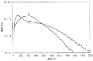
図4は半導体基板内の深さの関数としてのホウ素濃度に関して2種類の注入例を比較している。第一の例では、アンチモン、次いで二フッ化ホウ素次いでリンを使用した異なった3注入工程により実施した。アンチモン(Sb+)インプラントの運動エネルギーは30keV、投入量は2×1013cm-2および傾斜角は0°である。二フッ化ホウ素(BF2 +)インプラントの運動エネルギーは6keV、投入量は1×1015cm-2および傾斜角は0°である。リン(P+)インプラントの運動エネルギーは40keV、投入量は9×1013cm-2および傾斜角は15°である。第二の例では、アンチモンの注入後で二フッ化ホウ素の注入前にフッ素インプラントを追加的に注入したのを除けば第一の例と同様にして実施した。フッ素(F+)インプラントの運動エネルギーは30keV、投入量は1×1015cm-2および傾斜角は0°である。 FIG. 4 compares the two implant examples with respect to boron concentration as a function of depth in the semiconductor substrate. In the first example, it was performed by three different injection steps using antimony, then boron difluoride and then phosphorus. The kinetic energy of the antimony (Sb + ) implant is 30 keV, the input amount is 2 × 10 13 cm −2 and the inclination angle is 0 °. The kinetic energy of the boron difluoride (BF 2 + ) implant is 6 keV, the input dose is 1 × 10 15 cm −2 and the tilt angle is 0 °. The kinetic energy of the phosphorus (P + ) implant is 40 keV, the input is 9 × 10 13 cm −2 and the tilt angle is 15 °. The second example was carried out in the same manner as the first example, except that a fluorine implant was additionally injected after the injection of antimony and before the injection of boron difluoride. The kinetic energy of the fluorine (F + ) implant is 30 keV, the input amount is 1 × 10 15 cm −2 and the inclination angle is 0 °.
ソース・エクステンションおよび/あるいはドレイン・エクステンション内のドーパント濃度を半導体基板内の深さの関数として急峻に低下させることにより境界が明瞭な超薄型接合が形成される。図4に示されるように、アンチモンとフッ素のインプラントを両方とも二フッ化ホウ素インプラント前に注入した第二例の方が半導体基板内の深さの関数としてのドーパント濃度をより急峻に低下させた。このことは、第二例で形成された超薄型のドレイン・エクステンションあるいはソース・エクステンションとチャンネルの間の接合内での方がドーパント濃度はより急峻に低下することを意味する。更に図4に示されるように、第二例での方がホウ素濃度は基板内のより浅い点で10-17cm-3未満のレベルにまで低下しており、接合はより薄いことを意味している。従って、接合狭小化のための2種類の工程(すなわちアンチモンとフッ素の注入)は単一の接合狭小化工程を超えたメリットを提供する。 By sharply decreasing the dopant concentration in the source and / or drain extensions as a function of depth in the semiconductor substrate, a very thin junction with well defined boundaries is formed. As shown in FIG. 4, the second example, in which both antimony and fluorine implants were implanted before the boron difluoride implant, had a steeper drop in dopant concentration as a function of depth in the semiconductor substrate. . This means that the dopant concentration drops more abruptly in the junction between the ultra-thin drain extension or source extension formed in the second example and the channel. As further shown in FIG. 4, the boron concentration in the second example is reduced to a level less than 10 -17 cm -3 at a shallower point in the substrate, meaning that the junction is thinner. ing. Thus, the two types of junction narrowing steps (ie, antimony and fluorine implantation) provide advantages over a single junction narrowing step.
更に、第二例での2種類の接合狭小化工程はポケット分布に対してもメリットを提供する。図5は半導体基板内の深さの関数としてのリン濃度に関して図4で示されるのと同じ2種類の注入例を比較している。理想的には、ポケット分布は超薄型のドレイン・エクステンションおよび/あるいはドーパントのすぐ外側に存在し、チャンネル内には非常に遠くまでは侵入しない。図5に示されるように、2種類の接合狭小化工程を採用した第二例はこのような結果をもたらしている。第二例では、リン最大濃度は接合深さに対応する基板内の深さの点で達成されている。更に、第二例での方が基板内の深さの関数としてのリン濃度はより急峻に低下しており、このことは第一例でのポケット分布は第二例に比べてチャンネル内により深く浸透していることを意味している。 Furthermore, the two types of junction narrowing steps in the second example also provide benefits for pocket distribution. FIG. 5 compares the same two implant examples shown in FIG. 4 with respect to phosphorus concentration as a function of depth in the semiconductor substrate. Ideally, the pocket distribution is just outside the ultra-thin drain extension and / or dopant and does not penetrate very far into the channel. As shown in FIG. 5, the second example in which two types of junction narrowing processes are employed has such a result. In a second example, the maximum phosphorus concentration is achieved in terms of depth in the substrate corresponding to the junction depth. Further, the phosphorus concentration as a function of depth in the substrate is steeper in the second example, which means that the pocket distribution in the first example is deeper in the channel than in the second example. It means that it has penetrated.
第二例において2種類の接合狭小化工程は主ドーパント注入工程の前に実施したが、改善された結果が得られた正確な機構は不明である。接合狭小化工程のひとつあるいは両方共主ドーパント注入工程の後で実施したならば同じあるいはよりよい結果が得られた可能性がある。従って、本発明の好適な実施例は、主ドーパント注入工程に対する接合狭小化工程の前後関係を制限すると考えるべきではない。本発明の他の好適な実施例は、第一接合狭小化工程、主ドーパント注入工程および第二接合狭小化工程をこの順序で実施し次いでRTA工程を実施することにより超浅型接合を形成する。好ましくは、第一接合狭小化工程での接合狭小化種はアンチモン、ゲルマニウムおよび/あるいはケイ素により構成され、第二接合狭小化工程での接合狭小化種は炭素、フッ素、塩素、臭素および/あるいはヨウ素により構成される。本発明の更に他の好適な実施例は、主ドーパント注入工程、第一接合狭小化工程および第二接合狭小化工程をこの順序で実施し次いでRTA工程を実施することにより超浅型接合を形成する。追加的な注入工程(例えばポケット注入工程)あるいは追加的な接合狭小化工程も実施してよい。 In the second example, two types of junction narrowing steps were performed before the main dopant implantation step, but the exact mechanism by which improved results were obtained is not known. The same or better results may have been obtained if one or both of the junction narrowing steps were performed after the primary dopant implantation step. Therefore, the preferred embodiment of the present invention should not be considered to limit the context of the junction narrowing step relative to the main dopant implantation step. Another preferred embodiment of the present invention forms an ultra-shallow junction by performing a first junction narrowing step, a main dopant implanting step and a second junction narrowing step in this order, followed by an RTA step. . Preferably, the junction narrowing species in the first junction narrowing step is composed of antimony, germanium and / or silicon, and the junction narrowing species in the second junction narrowing step is carbon, fluorine, chlorine, bromine and / or It is composed of iodine. Yet another preferred embodiment of the present invention forms an ultra-shallow junction by performing a main dopant implantation step, a first junction narrowing step and a second junction narrowing step in this order, followed by an RTA step. I do. Additional implantation steps (eg, pocket implantation steps) or additional junction narrowing steps may also be performed.
以上、本発明の好適な実施態様を説明したが、当業界での熟練者は本発明の精神および説明事項を逸脱しない範囲内でこれらを変更することは可能である。特に、多くの接合狭小化工程が主ドーパント注入工程あるいは異なる接合狭小化工程の前あるいは後で実施可能であるので、多段の注入工程から構成される方法の言及はこれら工程の実施順序を制限するものではない。本明細書で記載された実施態様は本発明を説明するためのものであり制限しようとするものではない。ここに記載された本発明に対して多くの変更や修正が可能であり、これらは本発明の範囲内である。 The preferred embodiments of the present invention have been described above. However, those skilled in the art can modify them without departing from the spirit and description of the present invention. In particular, since many junction narrowing steps can be performed before or after the main dopant implantation step or different junction narrowing steps, reference to a method consisting of multiple implantation steps limits the order in which these steps are performed. Not something. The embodiments described herein are illustrative of the present invention and are not intended to be limiting. Many changes and modifications to the invention described herein are possible and are within the scope of the invention.
従って、保護範囲は上記の記載事項により制限されることはなく、下記の特許請求の範囲によってのみ制限され、その範囲は特許請求の主題と同等の全てのものを包含する。個々の特許請求項は全て本発明の実施態様として本明細書内に記載されている。従って、これらの特許請求項は本発明の好適な実施態様を更に説明し、かつこれら実施態様への追加物である。個々の特許請求項のどのような構成物に関してもそれに対して使用される「オプショナル」との言葉は、その構成物が必須であるか、あるいは必須ではないとの意味を意図している。いずれの場合であっても、特許請求の範囲内であることを意図している。「発明の背景」で引用された文献内での事項に言及したことは、これらが本発明の先行技術であることを認めたものではない。本発明の出願優先日以降に出版されたかもしれないどのような参照文献に関しては特にこのことが言える。本明細書内で引用された特許、特許出願および出版物は、本明細書内での記載事項を補足するための説明、方法あるいはその他の詳細を提供するために言及された。 Accordingly, the scope of protection is not limited by the above description, but is limited only by the following claims, which cover all equivalents of the claimed subject matter. All of the individual claims are set forth herein as embodiments of the present invention. Accordingly, these claims further describe preferred embodiments of the invention and are an addition to these embodiments. The term "optional," as used with respect to any component of a particular claim, is intended to mean that the component is or is not required. In each case, it is intended to be within the scope of the claims. The mention of matters in the documents cited in the "Background of the Invention" does not mean that they are prior art of the present invention. This is especially true for any reference that may have been published after the priority date of the present application. Patents, patent applications, and publications cited within this specification have been mentioned to provide clarification, methods, or other details that supplement the statements herein.
以上の説明に関して更に以下の項を開示する。
(1)以下の工程により半導体基板をドーピングすることを包含する、同基板内に超薄型(shallow:浅型)接合を形成する方法:
a.上記半導体基板の表面領域に第一の注入エネルギーによりアンチモンイオンを注入する;
b.上記表面領域に第二の注入エネルギーによりフッ素イオンを注入する;
c.上記表面領域に第一の注入エネルギーおよび第二の注入エネルギーより低い第三の注入エネルギーにより二フッ化ホウ素イオンを注入する;および
d.ホウ素ドーパントを高速熱アニール処理により活性化する。
(2)上記のアンチモン注入工程をフッ素注入工程および二フッ化ホウ素注入工程より前の段階で実施する(1)の方法。
(3)上記のフッ素注入工程を二フッ化ホウ素注入工程よりは前の段階で実施する(2)の方法。
(4)上記の二フッ化ホウ素注入工程をフッ素注入工程よりは前の段階で実施する(2)の方法。
(5)以下の条件下でイオン注入を実施する(1)の方法:
a.アンチモンイオンは運動(注入)エネルギー30〜35keV、投入量2×10¹³〜6×10¹³イオン/cm2で注入;
b.フッ素イオンは運動エネルギー12〜30keV、投入量5×10¹⁴〜2×10¹⁵イオン/cm2で注入;および
c.二フッ化ホウ素は運動エネルギー5〜6keV、投入量4×10¹⁴〜2×10¹⁵イオン/cm2で注入。
(6)以下の条件下でイオン注入を実施する(1)の方法:
a.アンチモンイオンは運動エネルギー5〜15keV、投入量1×10¹³〜5×10¹³イオン/cm2で注入;
b.フッ素イオンは運動エネルギー10〜20keV、投入量2×10¹⁵〜5×10¹⁵イオン/cm2で注入;および
c.二フッ化ホウ素は運動エネルギー1〜5keV、投入量4×10¹⁴〜2×10¹⁵イオン/cm2で注入。
(7)最上表面を有する半導体基板内に以下の構成を含む超薄型接合;
a.上記最上表面近傍の、実質的に上記最上表面に平行で実質的に平坦な部分を有する接合;
b.ホウ素原子、アンチモン原子およびフッ素原子を含有する、上記平坦な部分と最上表面との間の領域;および
c.上記領域内にフッ素原子はホウ素原子の2倍を超える数で存在する。
(8)上記接合近傍に存在するホウ素原子の密度が約1×10¹⁸原子/cm3である(7)の超薄型接合。
(9)上記実質的に平坦な部分が上記最上表面から約35〜50nmの距離にある(8)の超薄型接合。
(10)上記実質的に平坦な部分が上記最上表面から約28〜38nmの距離にある(8)の超薄型接合。
(11)複数のイオン注入工程を用いる半導体基板中に超薄型接合を形成する方法を開示する。イオン注入工程は、ホウ素のような少なくとも1つの電子活性ドーパントの注入を含み、フッ素(310)及びアンチモン(300)のような、ドーパント注入及び/又は熱拡散の間にチャンネリングにより接合が広がるのを制限する効果がある少なくとも2つの種の注入をも含む。ドーパント注入後に、電子的に活性なドーパントは、熱処理(330)により活性化される。
With respect to the above description, the following items are further disclosed.
(1) A method of forming an ultra-shallow (shallow) junction in a semiconductor substrate, including doping a semiconductor substrate by the following steps:
a. Implanting antimony ions into the surface region of the semiconductor substrate with a first implantation energy;
b. Implanting fluorine ions into the surface region with a second implantation energy;
c. Implanting boron difluoride ions into the surface region with a third implantation energy lower than the first implantation energy and the second implantation energy; and d. The boron dopant is activated by a rapid thermal anneal.
(2) The method according to (1), wherein the antimony implantation step is performed before the fluorine implantation step and the boron difluoride implantation step.
(3) The method according to (2), wherein the above-described fluorine implantation step is performed at a stage before the boron difluoride implantation step.
(4) The method according to (2), wherein the boron difluoride injection step is performed at a stage prior to the fluorine injection step.
(5) The method of (1) in which ion implantation is performed under the following conditions:
a. Antimony ions are implanted at a kinetic (implantation) energy of 30 to 35 keV and a dose of 2 × 10 13 to 6 × 10 13 ions / cm 2 ;
b. Fluorine ions are implanted at a kinetic energy of 12 to 30 keV and an input of 5 × 10 14 to 2 × 10 15 ions / cm 2 ; and c. Boron difluoride is implanted at a kinetic energy of 5 to 6 keV and an input of 4 × 10 14 to 2 × 10 15 ions / cm 2 .
(6) The method of (1) in which ion implantation is performed under the following conditions:
a. Antimony ions are implanted at a kinetic energy of 5 to 15 keV and an input of 1 × 10 13 to 5 × 10 13 ions / cm 2 ;
b. Fluorine ions are implanted at a kinetic energy of 10-20 keV and an input of 2 × 10 15 -5 × 10 15 ions / cm 2 ; and c. Boron difluoride is implanted at a kinetic energy of 1 to 5 keV and a dose of 4 × 10 14 to 2 × 10 15 ions / cm 2 .
(7) An ultra-thin junction including the following configuration in a semiconductor substrate having an uppermost surface;
a. A joint having a substantially flat portion near the top surface and substantially parallel to the top surface;
b. A region between the flat portion and the top surface containing boron, antimony and fluorine atoms; and c. Fluorine atoms are present in the above region in a number that is more than twice the number of boron atoms.
(8) The ultra-thin junction according to (7), wherein the density of boron atoms existing near the junction is about 1 × 10 18 atoms / cm 3 .
(9) The ultra-thin junction of (8), wherein the substantially flat portion is at a distance of about 35-50 nm from the top surface.
(10) The ultra-thin junction of (8), wherein the substantially flat portion is at a distance of about 28-38 nm from the top surface.
(11) A method for forming an ultra-thin junction in a semiconductor substrate using a plurality of ion implantation steps is disclosed. The ion implantation step includes the implantation of at least one electronically active dopant such as boron, such as fluorine (310) and antimony (300), that expands the junction by channeling during dopant implantation and / or thermal diffusion. And at least two species implants that have the effect of limiting After the dopant implantation, the electronically active dopant is activated by a heat treatment (330).
200 第一接合狭小化種注入工程
210 主ドーパント注入工程
230 ポケット注入工程(オプショナル)
220 高速熱アニール処理工程
300 第一接合狭小化種注入工程
310 第二接合狭小化種注入工程
320 主ドーパント注入工程
340 ポケット注入工程(オプショナル)
330 高速熱アニール処理工程
200 First junction narrowing
220 Rapid
330 Rapid thermal annealing process
Claims (2)
a.上記半導体基板の表面領域に第一の注入エネルギーによりアンチモンイオンを注入する;
b.上記表面領域に第二の注入エネルギーによりフッ素イオンを注入する;
c.上記表面領域に第一の注入エネルギーおよび第二の注入エネルギーより低い第三の注入エネルギーにより二フッ化ホウ素イオンを注入する;および
d.ホウ素ドーパントを高速熱アニール処理により活性化する。 A method of forming an ultra-thin junction in a semiconductor substrate, comprising doping a semiconductor substrate by the following steps:
a. Implanting antimony ions into the surface region of the semiconductor substrate with a first implantation energy;
b. Implanting fluorine ions into the surface region with a second implantation energy;
c. Implanting boron difluoride ions into the surface region with a third implantation energy lower than the first implantation energy and the second implantation energy; and d. The boron dopant is activated by a rapid thermal anneal.
a.上記最上表面近傍の、実質的に上記最上表面に平行で実質的に平坦な部分を有する接合;
b.ホウ素原子、アンチモン原子およびフッ素原子を含有する、上記平坦な部分と最上表面との間の領域;および
c.上記領域内にフッ素原子はホウ素原子の2倍を超える数で存在する。 An ultra-thin junction including the following features in a semiconductor substrate having a top surface:
a. A joint having a substantially flat portion near the top surface and substantially parallel to the top surface;
b. A region between the flat portion and the top surface containing boron, antimony and fluorine atoms; and c. Fluorine atoms are present in the above region in a number that is more than twice the number of boron atoms.
Applications Claiming Priority (1)
| Application Number | Priority Date | Filing Date | Title |
|---|---|---|---|
| US10/393,749 US6808997B2 (en) | 2003-03-21 | 2003-03-21 | Complementary junction-narrowing implants for ultra-shallow junctions |
Publications (2)
| Publication Number | Publication Date |
|---|---|
| JP2004289154A true JP2004289154A (en) | 2004-10-14 |
| JP2004289154A5 JP2004289154A5 (en) | 2007-04-12 |
Family
ID=32824912
Family Applications (1)
| Application Number | Title | Priority Date | Filing Date |
|---|---|---|---|
| JP2004079351A Abandoned JP2004289154A (en) | 2003-03-21 | 2004-03-19 | Complementary implant for narrowing junction for ultra-shallow junction |
Country Status (4)
| Country | Link |
|---|---|
| US (2) | US6808997B2 (en) |
| EP (1) | EP1460680B1 (en) |
| JP (1) | JP2004289154A (en) |
| DE (1) | DE602004031065D1 (en) |
Cited By (1)
| Publication number | Priority date | Publication date | Assignee | Title |
|---|---|---|---|---|
| WO2010103687A1 (en) * | 2009-03-09 | 2010-09-16 | 株式会社 東芝 | Semiconductor device and method for manufacturing same |
Families Citing this family (16)
| Publication number | Priority date | Publication date | Assignee | Title |
|---|---|---|---|---|
| US20050260838A1 (en) * | 2002-05-10 | 2005-11-24 | Varian Semiconductor Equipment Associates, Inc. | Methods and systems for dopant profiling |
| US6767809B2 (en) * | 2002-11-19 | 2004-07-27 | Silterra Malayisa Sdn. Bhd. | Method of forming ultra shallow junctions |
| CN1253929C (en) * | 2003-03-04 | 2006-04-26 | 松下电器产业株式会社 | Semiconductor device and producing method thereof |
| US20060017079A1 (en) * | 2004-07-21 | 2006-01-26 | Srinivasan Chakravarthi | N-type transistor with antimony-doped ultra shallow source and drain |
| US7482255B2 (en) * | 2004-12-17 | 2009-01-27 | Houda Graoui | Method of ion implantation to reduce transient enhanced diffusion |
| CN101207020B (en) * | 2006-12-22 | 2010-09-29 | 中芯国际集成电路制造(上海)有限公司 | Method for forming ultra-shallow junction |
| US7888223B2 (en) * | 2007-03-28 | 2011-02-15 | United Microelectronics Corp. | Method for fabricating P-channel field-effect transistor (FET) |
| US8664073B2 (en) | 2007-03-28 | 2014-03-04 | United Microelectronics Corp. | Method for fabricating field-effect transistor |
| US20090065820A1 (en) * | 2007-09-06 | 2009-03-12 | Lu-Yang Kao | Method and structure for simultaneously fabricating selective film and spacer |
| US8232605B2 (en) * | 2008-12-17 | 2012-07-31 | United Microelectronics Corp. | Method for gate leakage reduction and Vt shift control and complementary metal-oxide-semiconductor device |
| US8178430B2 (en) | 2009-04-08 | 2012-05-15 | International Business Machines Corporation | N-type carrier enhancement in semiconductors |
| US8269275B2 (en) * | 2009-10-21 | 2012-09-18 | Broadcom Corporation | Method for fabricating a MOS transistor with reduced channel length variation and related structure |
| US8564063B2 (en) | 2010-12-07 | 2013-10-22 | United Microelectronics Corp. | Semiconductor device having metal gate and manufacturing method thereof |
| CN102637646B (en) * | 2011-02-10 | 2014-04-23 | 上海宏力半导体制造有限公司 | Preparation method of memory |
| US8772118B2 (en) | 2011-07-08 | 2014-07-08 | Texas Instruments Incorporated | Offset screen for shallow source/drain extension implants, and processes and integrated circuits |
| US9455321B1 (en) | 2015-05-06 | 2016-09-27 | United Microelectronics Corp. | Method for fabricating semiconductor device |
Family Cites Families (17)
| Publication number | Priority date | Publication date | Assignee | Title |
|---|---|---|---|---|
| JPH1079506A (en) * | 1996-02-07 | 1998-03-24 | Matsushita Electric Ind Co Ltd | Semiconductor device and its manufacturing method |
| KR0183645B1 (en) | 1996-03-26 | 1999-03-20 | 이대원 | Semiconductor leadframe having composite plating |
| EP0897594B1 (en) | 1996-05-08 | 2004-07-28 | Advanced Micro Devices, Inc. | Control of junction depth and channel length using generated interstitial gradients to oppose dopant diffusion |
| US5793090A (en) | 1997-01-10 | 1998-08-11 | Advanced Micro Devices, Inc. | Integrated circuit having multiple LDD and/or source/drain implant steps to enhance circuit performance |
| US6069062A (en) | 1997-09-16 | 2000-05-30 | Varian Semiconductor Equipment Associates, Inc. | Methods for forming shallow junctions in semiconductor wafers |
| US6037640A (en) * | 1997-11-12 | 2000-03-14 | International Business Machines Corporation | Ultra-shallow semiconductor junction formation |
| US6087247A (en) | 1998-01-29 | 2000-07-11 | Varian Semiconductor Equipment Associates, Inc. | Method for forming shallow junctions in semiconductor wafers using controlled, low level oxygen ambients during annealing |
| US6355543B1 (en) | 1998-09-29 | 2002-03-12 | Advanced Micro Devices, Inc. | Laser annealing for forming shallow source/drain extension for MOS transistor |
| US6180476B1 (en) | 1998-11-06 | 2001-01-30 | Advanced Micro Devices, Inc. | Dual amorphization implant process for ultra-shallow drain and source extensions |
| KR100318459B1 (en) | 1998-12-22 | 2002-02-19 | 박종섭 | A method for forming titanium polycide gate electrode |
| EP1269223A4 (en) * | 2000-01-26 | 2003-03-26 | Sola Int Holdings | Anti-static, anti-reflection coating |
| US6265255B1 (en) | 2000-03-17 | 2001-07-24 | United Microelectronics Corp. | Ultra-shallow junction formation for deep sub-micron complementary metal-oxide-semiconductor |
| US6358823B1 (en) | 2000-04-12 | 2002-03-19 | Institut Fuer Halbleiterphysik Frankfurt (Oder) Gmbh. | Method of fabricating ion implanted doping layers in semiconductor materials and integrated circuits made therefrom |
| JP2002076332A (en) * | 2000-08-24 | 2002-03-15 | Hitachi Ltd | Insulating gate field effect transistor and manufacturing method therefor |
| US6534373B1 (en) * | 2001-03-26 | 2003-03-18 | Advanced Micro Devices, Inc. | MOS transistor with reduced floating body effect |
| US6458643B1 (en) * | 2001-07-03 | 2002-10-01 | Macronix International Co. Ltd. | Method of fabricating a MOS device with an ultra-shallow junction |
| CN1253929C (en) * | 2003-03-04 | 2006-04-26 | 松下电器产业株式会社 | Semiconductor device and producing method thereof |
-
2003
- 2003-03-21 US US10/393,749 patent/US6808997B2/en not_active Expired - Lifetime
-
2004
- 2004-03-18 EP EP04101123A patent/EP1460680B1/en not_active Expired - Fee Related
- 2004-03-18 DE DE602004031065T patent/DE602004031065D1/en not_active Expired - Lifetime
- 2004-03-19 JP JP2004079351A patent/JP2004289154A/en not_active Abandoned
- 2004-09-15 US US10/942,607 patent/US7345355B2/en not_active Expired - Lifetime
Cited By (2)
| Publication number | Priority date | Publication date | Assignee | Title |
|---|---|---|---|---|
| WO2010103687A1 (en) * | 2009-03-09 | 2010-09-16 | 株式会社 東芝 | Semiconductor device and method for manufacturing same |
| JP2012099510A (en) * | 2009-03-09 | 2012-05-24 | Toshiba Corp | Semiconductor device and method of manufacturing the same |
Also Published As
| Publication number | Publication date |
|---|---|
| EP1460680B1 (en) | 2011-01-19 |
| EP1460680A3 (en) | 2005-08-17 |
| EP1460680A2 (en) | 2004-09-22 |
| US20040185633A1 (en) | 2004-09-23 |
| US6808997B2 (en) | 2004-10-26 |
| US7345355B2 (en) | 2008-03-18 |
| DE602004031065D1 (en) | 2011-03-03 |
| US20050042848A1 (en) | 2005-02-24 |
Similar Documents
| Publication | Publication Date | Title |
|---|---|---|
| KR100305623B1 (en) | Fabrication method of semiconductor device using ion implantation | |
| JP4708563B2 (en) | Method for reducing the effective channel length of a lightly doped drain transistor and method for forming a transistor | |
| US6682980B2 (en) | Fabrication of abrupt ultra-shallow junctions using angled PAI and fluorine implant | |
| JP2004289154A (en) | Complementary implant for narrowing junction for ultra-shallow junction | |
| KR100768500B1 (en) | A process for forming an ultrashallow junction in a semiconductor substrate as an integral part of a semiconductor device | |
| JP2005510085A (en) | Method for forming an ultra-shallow junction | |
| US6063682A (en) | Ultra-shallow p-type junction having reduced sheet resistance and method for producing shallow junctions | |
| JP2008510300A (en) | Ultra shallow junction formation method | |
| JP2020535632A (en) | Reduction of series resistance between source and / or drain regions and channel regions | |
| US20100015788A1 (en) | Method for manufacturing semiconductor device | |
| Foad et al. | Formation of ultra-shallow junctions by ion implantation and RTA | |
| WO2005096357A1 (en) | Method for manufacturing semiconductor device | |
| US20080308904A1 (en) | P-doped region with improved abruptness | |
| US7479668B2 (en) | Source/drain extension implant process for use with short time anneals | |
| US6767809B2 (en) | Method of forming ultra shallow junctions | |
| JPH0689870A (en) | Manufacture of semiconductor element | |
| KR100212010B1 (en) | Method for fabricating transistor of semiconductor device | |
| JP2000100746A (en) | Forming of diffused layer | |
| JP2700320B2 (en) | Method for manufacturing semiconductor device | |
| JP2781989B2 (en) | Method for manufacturing semiconductor device | |
| JPH06151348A (en) | Manufacture of semiconductor device | |
| JPH098310A (en) | Fabrication of semiconductor device | |
| JPH0689869A (en) | Manufacture of semiconductor element | |
| CN101567319A (en) | Production method of transistors | |
| JP2005347731A (en) | Semiconductor device and manufacturing method therefor |
Legal Events
| Date | Code | Title | Description |
|---|---|---|---|
| A521 | Written amendment |
Free format text: JAPANESE INTERMEDIATE CODE: A523 Effective date: 20070226 |
|
| A621 | Written request for application examination |
Free format text: JAPANESE INTERMEDIATE CODE: A621 Effective date: 20070226 |
|
| A762 | Written abandonment of application |
Free format text: JAPANESE INTERMEDIATE CODE: A762 Effective date: 20090924 |